氟離子佈植對低溫多晶矽薄膜電晶體之研究
90
0
0
全文
(2) 氟離子佈植對低溫多晶矽薄膜電晶體之研究 The Study on Fluorine Ion Implanted Poly-Si Thin Film Transistors 研 究 生:楊哲育. Student:Che-Yu Yang. 指導教授:張俊彥 博士. Advisor:Dr. Chun-Yen Chang. 張鼎張 博士. Dr. Ting-Chang Chang 國立交通大學. 電子工程學系. 電子研究所碩士班. 碩 士 論 文. A Thesis Submitted to Department of Electronics Engineering & Institute of Electronics College of Electrical Engineering and Computer Science National Chiao Tung University in partial Fulfillment of the Requirements for the Degree of Master in Electronics Engineering June 2005 Hsinchu, Taiwan, Republic of China. 中華民國九十四年六月.
(3) 氟離子佈植對低溫多晶矽薄膜電晶體之研究. 研究生:楊哲育. 指導教授:張俊彥&張鼎張 國立交通大學. 電子工程學系 電子研究所碩士班. 摘要. 本論文主要在研究氟離子佈值對多晶矽薄膜電晶體特性的影 響,在製程步驟上,我們並不沉積櫬墊氧化層(pad oxide)來使氟離 子堆積在多晶矽通道與氧化層介面,而是直接利用熱退火步驟產生的 氧化層來代替積櫬墊氧化層的角色,因而能在減少製程的步驟情況 下,同樣得到氟離子鈍化(passivation)缺陷的效果。 13. -2. 由實驗結果顯示在 5x10 cm 的劑量下,不管是利用固相結晶法 (solid phase crystallization) , 或 是 準 分 子 雷 射 退 火 結 晶 法 (excimer laser annealing)製作的元件,其特性將得到改善,包括 較高的遷移率(mobility)、開關電流比(on/off ratio)、較陡峭的次 臨 界 導 通 斜 率 (subthreshold swing) 與 較 佳 的 可 靠 度 (relibility)。這是由於氟離子可以打斷扭曲的鍵結,如矽-氧-矽或. I.
(4) 矽-矽的鍵結,形成強度較高的矽-氟鍵,使應力得到舒緩,以減少tail state的數目,氟離子也會和一些斷鍵(dangling bonds)鍵結,讓deep state的數目降低,此外,由於矽-氟鍵的鍵結強度比矽-氫鍵結高, 因而能得到比一般薄膜電晶體更佳的可靠度。實驗結果也顯示當劑量 增加時,元件的特性將反而劣化,由萃取缺陷密度的結果,我們發現 過量的氟離子反而會導致較高的缺陷密度,因而使元件的電性劣化。 由於此製程只需外加一道氟離子佈植的製程,因此可以較低的製 程成本與複雜度來達到元件效能的提升,此元件可被運用於高效能的 複晶矽薄膜電晶體之運用,尤其是在主動式薄膜電晶體液晶顯示器 (AMLCD) ,以及三維立體的金氧半場效電晶體電路。. II.
(5) The Study on Fluorine Ion Implanted Poly-Si Thin Film Transistors Student :Che-Yu Yang Advisor :Dr. Chun-Yen Chang & Dr. Ting-Chang Chang. Department of Electronics & Institute of Electronics, National Chiao Tung University. Abstract In this thesis, Polycrystalline silicon thin film transistors (Poly-Si TFTs) with fluorine ion implantation was investigated. In the process step, we used the surface-oxidized Si generated during thermal annealing in place of the pad oxide to make the drive force for fluorine atoms segregated to the poly-Si/oxide interface. Compared to the conventional fluorine incorporated poly-Si TFTs technology, the method we proposed needed no extra thermal annealing step and additional process steps. From the experiment result, it is found that the electrical characteristics of solid phase re-crystallized (SPC) and excimer laser annealing (ELA) fluorine ion implanted poly-Si TFTs will be improved, such as a higher mobility (µFE), a higher on/off current ratio (Ion/Ioff), a steep subthreshold swing (S.S) and a improved reliability. It is believed that the fluorine atoms can break the stress induced strained bonds, likely III.
(6) the strained Si-O-Si bonds and Si-Si bonds to form stronger Si-F bonds, leading to local stress relaxation and thus decreasing the tail state density. Moreover, the fluorine atoms in the poly-Si channel can also passivate the dangling bonds to decrease deep state density. In addition, the Si-F bonds is stronger than Si-H bonds, result in the improved reliability compared to conventional TFT. Experiment result show that the over amount of fluorine ion implantation doses cause the degraded electrical characteristics, result from the increase of the trap state density. This process only needs to increase one additional fluorine ion implantation process. The device can be improved by low cost and complication. Such TFTs are thus highly promising for use in future high-performance poly-Si TFT applications, especially in AMLCD and 3D MOSFET stacked circuits.. IV.
(7) Acknowledgement. 僅以此篇論文獻給我親愛的父母,感謝他們多年來的支持與鼓 勵,讓我能無後顧之憂的從事實驗研究,順利完成我的學業。 在交大求學的這兩年中,要特別感謝我的兩位指導教授,張俊彥 教授是一位名滿中外的學者,他在學術研究的精神和追求卓越創新的 勇氣值得我多加學習。另外,也感謝張鼎張教授的殷勤指導,在我遇 到困難時指點我新的想法、鼓勵我、支持我。有機會能接受這兩位老 師的指導,實在是學生的福氣,在此獻上最高的敬意與謝意。 此外更感謝涂俊豪與吳永俊兩位學長在這段期間給我的指導與 幫助,從實驗流程、分析結果到論文寫作等各方面都使我獲益良多。 還要感謝實驗室吳師道學長、楊中熹學長、彭辭修學長與陳漢譽學長 等平日對我的照顧,還有劉柏村博士、陳紀文學長、陳世青學長、吳 興華學長、張保安學長等在儀器與實驗方面的傳授教導。 同時要感謝和我一起奮鬥的同學,立偉、武陵、道彥、兆欽等… 由於各位的勉勵和幫助才讓此論文得以如期完成。最後感謝國家奈米 元件實驗室提供良好的設備和研究環境,以及相關人員的協助。. V.
(8) Contents Ⅰ. Chinese abstract English abstract. Ⅲ. Acknowledgement(Chinese). Ⅴ. Contents. Ⅵ. Figure captions. Ⅸ ⅩIII. Table lists Chapter 1.. Introduction. 1. 1-1.. Overview of Polysilicon Thin-Film Transistor Technology. 1. 1-2.. Defects in Poly-Si Film. 3. 1-3.. Motivation. 4. 1-4.. Thesis Outline. 5. Chapter 2. Poly-Si conduction mechanism. 7. 2-1.. Transport properties of poly-Si. 2-2.. Non-ideal effect. 10. 2-2-1. Leakage current. 11. 2-2-2. Kink effect. 11. Chapter 3.. Experiment. 7. 13. 3-1.. Fabrication process of poly-Si TFTs. 13. 3-2.. Measurement. 17. 3-3.. Methods of device parameter extraction. 17. 3-3-1. Determination of the threshold voltage. 17. VI.
(9) 3-3-2. Determination of the subthreshold swing. 18. 3-3-3. Determination of On/Off current ratio. 18. 3-3-4. Determination of the field-effect mobility. 19. 3-3-5. Determination of the poly-Si grain boundary trap density. 20. Chapter 4. 4-1.. Results and discussion. 22. Poly-silicon thin-film transistors fabricated by solid phase crystallization method. 22. 4-1-1. Device characteristic of poly-silicon TFTs. 22. 4-1-2. The effects of fluorine passvation. 23. 4-1-3. The activation energy variation with fluorine incorporation. 25. 4-1-4. Stress result of poly-Si TFTs with/without fluorine implantation 4-2.. 26. Poly-silicon thin-film transistor fabricated by excimer laser annealing method. 28. 4-2-1. Device characteristic of poly-silicon TFTs. 28. 4-2-2. The effects of fluorine passvation. 29. 4-2-3. The activation energy variation with fluorine incorporation. 30. 4-2-4. Stress result of poly-Si TFTs with/without fluorine implantation 4-3.. 30. Comparison between SPC and ELA Poly-Silicon Thin Film Transistors. 31. 4-3-1. Comparison of the electrical characteristics improvement. 31. 4-3-2. Comparison of the reliability between ELA and SPC TFTs. 32. VII.
(10) Chapter 5. Conclusion. 33. Reference. 34. Figures. 40. VIII.
(11) Figure captions Chapter 2 Fig. 2-1. Sketch of the band diagram of the polycrystalline silicon films. Fig. 2-2. A schematic MOSFET cross section, showing the axes of coordinates and the bias voltages at the four terminals for the drain-current model.. Fig. 2-3. Three possible mechanisms of leakage current in poly-Si TFTs, including thermionic emission, thermionic field emission and pure tunneling. Fig. 2-4. The kink effect in the output characteristics of an n-channel SOI MOSFET. Chapter 3 Fig. 3-1. The top view of TFT. Fig. 3-2. Cross-section view of TFT. Chapter 4 Fig.4-1. Transfer characteristic for fluorine implanted TFT and standard TFT at VD=0.1V. Fig.4-2. Transfer characteristic for fluorine implanted TFT and standard TFT at VD =5V. Fig.4-3. Field effect mobility (µFE) versus different fluorine implantation dosage poly-Si TFTs.. Fig.4-4. Threshold voltage (VTH) versus different fluorine implantation dosage poly-Si TFTs.. Fig.4-5. Subthreshold swing (S.S) versus different fluorine implantation dosage poly-Si TFTs.. Fig.4-6. Ion/Ioff ratio versus different fluorine implantation dosage poly-Si TFTs.. Fig.4-7. Output characteristic for fluorine implanted TFT and standard TFT.. IX.
(12) Fig.4-8. Secondary-ion mass spectrometry (SIMS) depth profile with various fluorine ion implantation doses after solid phase re-crysatllization(600℃ for 24 hrs).. Fig.4-9. Trap state density (Nt) versus different fluorine implantation dosage poly-Si TFTs.. Fig.4-10. The scanning electron microscope (SEM) image of poly-Si grain with different fluorine doses after SPC method.. Fig.4-11. The activation energy of drain current as a function of gate voltage measured at VD =5 V for standard and fluorine ion implanted poly-Si TFTs. Fig.4-12. Threshold voltage variation (ΔVTH) of SPC poly-Si TFTs with/without fluorine implantation versus stress time under a stress voltage VD=VG=20V.. Fig.4-13 On-current degradation of SPC poly-Si TFTs with/without fluorine implantation versus stress time under a stress voltage VD=VG=20V. Fig.4-14. Subthreshold swing variation (ΔS.S) of SPC poly-Si TFTs with/without fluorine implantation versus stress time under a stress voltage VD=VG=20V.. Fig.4-15 Transfer characteristic for fluorine implanted TFT and standard TFT at VD =0.1V Fig.4-16 Transfer characteristic for fluorine implanted TFT and standard TFT at VD =5V Fig.4-17. Field effect mobility (µFE) versus different fluorine implantation dosage poly-Si TFTs.. Fig.4-18. Threshold voltage (VTH) versus different fluorine implantation dosage poly-Si TFTs.. Fig.4-19. Subthreshold swing (S.S) versus different fluorine implantation dosage X.
(13) poly-Si TFTs. Fig.4-20. Ion/Ioff ratio versus different fluorine implantation dosage poly-Si TFTs.. Fig.4-21 Output characteristic for fluorine implanted TFT and standard TFT. Fig.4-22. Secondary-ion mass spectrometry (SIMS) depth profile with various fluorine ion implantation doses after excimer laser re-crysatllization.. Fig.4-23. The scanning electron microscope (SEM) image of poly-Si grain with different fluorine doses after ELA method.. Fig.4-24. Trap state density (Nt) versus different fluorine implantation dosage poly-Si TFTs.. Fig.4-25. The activation energy of drain current as a function of gate voltage measured at VD=5 V for standard and fluorine ion implanted poly-Si TFTs. Fig.4-26. Threshold voltage variation (ΔVth) of poly-Si ELA TFTs with/without fluorine implantation versus stress time under a stress voltage VD=VG=20V.. Fig.4-27 On-current degradation of ELA poly-Si TFTs with/without fluorine implantation versus stress time under a stress voltage Vd=Vg=20V. Fig.4-28. Subthreshold swing variation (ΔS.S) of ELA poly-Si TFTs with/without fluorine implantation versus stress time under a stress voltage VD=VG=20V.. Fig.4-29. Threshold voltage variation (ΔVth) of ELA and SPC poly-Si TFTs with/without fluorine implantation versus stress time under a stress voltage VD=VG=20V.. Fig.4-30 On-current degradation of ELA and SPC poly-Si TFTs with/without fluorine implantation versus stress time under a stress voltage VD=VG=20V. Fig.4-31. Subthreshold swing variation (ΔS.S) of ELA and SPC poly-Si TFTs with/without fluorine implantation versus stress time under a stress voltage XI.
(14) VD=VG=20V.. XII.
(15) Table lists. Chapter 4 Table I. Device parameters for standard SPC TFT and fluorine implanted SPC TFT, including mobility, threshold voltage(VTH), subthreshold swing(S.S), Ion/Ioff ratio and trap state density(Nt). All parameters were extracted at VD=0.1V. TableⅡ The association energy of the different bonding Table Ⅲ Device parameters for standard ELA TFT and fluorine implanted ELA TFT, including mobility, threshold voltage(VTH), subthreshold swing(S.S), Ion/Ioff ratio and trap state density(Nt). All parameters were extracted at VD=0.1V Table Ⅳ The electrical characteristics improvement by fluorine implantation of SPC and ELA poly-Si TFTs Table Ⅴ The relation between the electrical parameter and the location of the trap states.. XIII.
(16) Chapter 1 Introduction. 1-1. Overview of Poly-silicon Thin-Film Transistor Technology. In recent years, polycrystalline silicon thin-film transistors (poly-Si TFTs) have drawn much attention because of their widely applications on active matrix liquid crystal displays (AMLCDs) [1], and organic light-emitting displays (OLEDs) [2]. Except large area displays, poly-Si TFTs also have been applied into some memory devices such as dynamic random access memories (DRAMs) [3], static random access memories (SRAMs) [4], electrical programming read only memories (EPROM) [5], electrical erasable programming read only memories (EEPROMs) [6], linear image sensors [7], thermal printer heads [8], photo-detector amplifier [9], scanner [10], neutral networks [10]. Lately, some superior performances of poly-Si TFTs also have been reported by scaling down device dimension or utilizing novel crystallization technologies to enhance poly-Si film quality [11-12]. This provides the opportunity of using poly-Si TFTs into three-dimension (3-D) integrated circuit fabrication. Of course, the application in AMLCDs is the primary trend, leading to rapid developing of poly-Si TFT technology. The major attraction of applying polycrystalline silicon thin-film transistors (poly-Si TFTs) in active matrix liquid crystal display (AMLCDs) lies in the greatly improved carrier mobility in poly-Si film and the capability of integrating the pixel switching elements and the capability to integrate panel array and peripheral driving circuit on the same substrates [13-15]. In poly-Si film, carrier mobility larger than 15 1.
(17) cm2/Vs can be easily achieved, that is enough to used as peripheral driving circuit including n- and p-channel devices. This enables the fabrication of peripheral circuit and TFT array on the same glass substrate, bring the era of system-on-glass (SOG) technology. The process complexity can be greatly simplified to lower the cost. In addition, the mobility of poly-Si TFTs is much better than that of amorphous ones, the dimension of the poly-Si TFTs can be made smaller compared to that of amorphous Si TFTs for high density、high resolution AMLCDs, and the aperture ratio in TFT array can be significantly improved by using poly-Si TFTs as pixel switching elements. This is because that the device channel width can be scaled down while meeting the same pixel driving requirements as in α-Si TFT AMLCDs. For making high performance poly-crystalline silicon (poly-Si) thin film transistors (TFTs) [16], low-temperature technology is required for the realization of commercial flat-panel displays (FPD) on inexpensive glass substrate, since the maximum process temperature is limited to less than 6000C. There three major low-temperature amorphous-Si crystallization methods to achieve high performance poly-Si thin film, solid phase crystallization (SPC), excimer laser crystallization (ELC), and Metal-Induced Lateral Crystallization (MILC) However, some problems still exist in applying poly-Si TFTs on large-area displays. In comparison with single-crystalline silicon, poly-Si is rich in grain boundary defects as well as intra-grain defects, and the electrical activity of the charge-trapping centers profoundly affects the electrical characteristics of poly-Si TFTs. Large amount of defects serving as trap states locate in the disordered grain boundary regions to degrade the ON current seriously [17]. Moreover, the relatively large leakage current is one of the most important issues of conventional poly-Si TFTs under OFF-state operation [18-19]. In most application, a low-cost substrate is essential and therefore a low temperature process (i.e., <650°C) compatible with glass 2.
(18) substrates is developed [20]. In summary, it is expected that the poly-Si TFTs will becomes more important in future technologies, especially when the 3-D circuit integration era is coming. More researches studying the related new technologies and the underlying mechanisms in poly-Si devices with shrinking dimensions are therefore worthy to be indulged in.. 1-2. Defects in Poly-Si Film. Due to the granular structure of the poly-Si film, a lot of grain boundaries and intragranular defects exist in the film. The dangling bonds in grain boundaries will affect device characteristics seriously because they act as trapping centers to trap carriers. Carriers trapped by these low energy traps can no longer contribute to conduction, which results in the formation of local depletion region and potential barriers in these grain boundaries. Thus, the typical characteristics such as threshold voltage, subthreshold swing, ON current, mobility and transconductance of TFTs are inferior to those of devices fabricated on single crystal silicon film. As for the leakage current, it is well known that the leakage current increase with the drain voltage and gate voltage. The dominant mechanism of the leakage current is field emission via grain boundary traps due to the high electric field near the drain junction [21-24]. To overcome this inherent disadvantage of poly-Si film, many researches have been focused on modifying or eliminating these grain boundary traps. Traps are associated with dangling bonds arising from lattice discontinuities between different oriented grains or at the Si/SiO2 interface. The most useful method so far to remove traps is to passivate these dangling bonds, such as hydrogen plasma treatment has been utilized for the passivation [25-26], but it is difficult to control the hydrogen 3.
(19) concentration in the TFT. The Si-H bonds may be broken under hot-carrier stress [27-28], leading to degradation of electrical characteristics after a long-term operation time. As the number of trapped carrier decreases, the potential barriers in grain boundaries decrease. And the leakage current decreases because of the fewer trap density near the drain region.. 1-3. Motivation. To meet the requirement of higher circuit density and higher speed, it is necessary to improve the performance of the poly-Si TFTs. However, it has been shown that the performances of poly-Si are affected by the trap states at grain boundaries. In the preview research, Enlarging the grain size and passivating the defects at the grain boundary were widely used methods to reduce the trap states in the grain boundary. Generally, hydrogen plasma treatment has been utilized for the passivation, but it is difficult to control the hydrogen concentration in the TFTs. In recent years, fluorine ion implantation was applied to improve the electrical characteristics by eliminating the defects in the grain boundary [29-30]. It is found that the fluorine atoms piled up at the interface between the poly-Si and oxide to break the stress induced strained bonds to form stronger Si-F bonds, leading to local stress relaxation and thus decreasing the tail state density [31]. The fluorine atoms can also be the terminator of dangling bonding in poly-Si. Hence, the TFT with fluorine implantation has the superior electrical characteristics than conventional poly-Si TFTs. However, it needs additional oxide layer deposition and additional thermal annealing. The extra process steps will increase the difficulty for the fabrication of poly-Si TFTs. In this work, the electrical characteristics behaviors of poly-Si TFTs by various 4.
(20) fluorine ion implantation dosages were investigated. In addition, there was no any pad oxide deposited firstly before thermal annealing. Hence, it also needed no additional thermal annealing step. The electrical characteristics, including I-V measurement and DC bias stress reliability, were reported in this study.. 1-4. Thesis Outline Chapter 1.. Introduction. 1-1.. Overview of Polysilicon Thin-Film Transistor Technology. 1-2.. Defects in Poly-Si Film. 1-3.. Motivation. 1-4.. Thesis Outline. Chapter 2.. Poly-Si conduction mechanism. 2-1.. Transport Properties of Poly-Si. 2-2.. Non-ideal Effect. Chapter 3.. Experiment. 3-1.. Fabrication Process of Poly-Si TFT. 3-2.. Measurement. 3-3.. Methods of Device Parameter Extraction. Chapter 4. 4-1.. Results and discussion. Poly-Silicon Thin-Film Transistor Fabricated by Solid Phase Crystallization (SPC) Method. 4-2.. Poly-Silicon Thin-Film Transistor Fabricated by Excimer Laser Annealing. 5.
(21) (ELA) Method 4-3.. Comparison Between SPC and ELA Poly-Silicon Thin Film Transistors. Chapter 5.. Conclusion. 6.
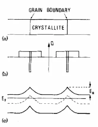
(22) Chapter 2 Poly-Si conduction mechanism. 2-1. Transport Properties of Poly-Si. As mentioned in section 1-1 and 1-2, the device characteristics of poly-Si TFTs are strongly influenced by the grain structure in poly-Si film. Even though the inversion channel region is also induced by the gate voltage as in MOSFETs, the existence of grain structure in channel layer bring large differences in carrier transport phenomenon. Many researches studying the electrical properties and the carrier transport in poly-Si TFTs have been reported. A simple grain boundary-trapping model has been described by many authors in details [1-3]. In this model, it is assumed that the poly-Si material is composed of a linear chain of identical crystallite having a grain size Lg and the grain boundary trap density Nt. The charge trapped at grain boundaries is compensated by oppositely charged depletion regions surrounding the grain boundaries. It is shown in Figure. 2-1. From Poisson’s equation, the charge in the depletion regions causes curvature in the energy bands, leading to potential barriers that impede the movement of any remaining free carriers from one grain to another. When the dopant/carrier density n is small, the poly-Si grains will be fully. 7.
(23) depleted. The width of the grain boundary depletion region xd extends to be Lg/2 on each side of the boundary, and the barrier height VB can be expressed as qn 2 qnL g VB = xd = 2ε s 8ε s. 2. (2-1). As the dopant/carrier concentration is increased, more carriers are trapped at the grain boundary. The curvature of the energy band and the height of potential barrier increase, making carrier transport form one grain to another more difficult. When the dopant/carrier density increases to exceed a critical value N* = Nt / Lg, the poly-Si grains turn to be partially depleted and excess free carriers start to spear inside the grain region. The depletion width and the barrier height can be expressed as xd =. Nt 2n. (2-2) 2. qn N t 2 qN t ( ) = VB = 2ε s 2n 8ε s n. (2-3). The depletion width and the barrier height turn to decrease with increasing dopant/carrier density, leading to improved conductivity in carrier transport. The carrier transport in fully depleted poly-Si film can be described by the thermionic emission over the barrier. Its’ current density can be written as [4].. J = qnvc exp[−. q (VB − V )] kT. (2-4). where n is the free-carrier density, vc is the collection velocity ( vc = kT / 2πm ∗ ), VB is the barrier height without applied bias, and Vg is the applied bias across the grain. 8.
(24) boundary region. For small applied biases, the applied voltage divided approximately uniformly between the two sides of a grain boundary. Therefore, the barrier in the forward-bias direction decreases by an amount of Vg/2. In the reserve-bias direction, the barrier increases by the same amount. The current density in these two directions then can be expressed as J F = qnvc exp[−. q 1 (VB − Vg ] kT 2. (2-5). J R = qnvc exp[−. q 1 (VB + Vg )] kT 2. (2-6). the net current density is then given by J = 2qnv c exp(−. qV g qV B ) sinh( ) kT 2kT. (2-7). at low applied voltages, the voltage drop across a grain boundary is small compared to the thermal voltage kT/q, Eq. (1.7) then can be simplified as J = 2qnv c exp( −. 2 qV B qV g q nv cV g qV ) = [exp(− B )] kT kT kT 2kT. (2-8). the average conductivity σ = J / Ε = JLg / Vg and the effective mobility µeff = σ / qn then can be obtained. σ=. q 2 nvc Lg. µ eff =. kT qv c L g kT. exp(−. qVB ) kT. (2-9). exp(−. qV B qV ) ≡ µ 0 exp(− B ) kT kT. (2-10). where µ0 represents the carrier mobility inside grain regions. It is found that the conduction in poly-Si is an activated process with activation energy of approximately qVB, which depends on the dopant/carrier concentration and the grain boundary trap. 9.
(25) density. Applying gradual channel approximation to poly-Si TFTs, which assumes that the variation of the electric field in the y-direction (along the channel) is much less than the corresponding variation in the z-direction (perpendicular to the channel), as shown Fig. 2-2. The carrier density n per unit area (cm-2) induced by the gate voltage can be expressed as n=. Cox (VG − VTH − V( y ) ). (2-11). qtch. I D = ∫∫ J .dx.dz = ∫∫ nqµeff . W. tch. 0. 0. = ∫ µeff dz ∫ nqdx.. dVy dy. dv y dy. .dx.dz. (2-12). = W µ eff .Cox (Vg − Vth − Vy ). dVy dy. where tch is the thickness of the inversion layer. Therefore, the drain current ID of poly-Si TFT then can be given by. ∫. L. 0. 1 I D dy = W µ ff Cox ⎡⎣(Vg − Vth ) VD − VD 2 ⎤⎦ 2. ID =. W 1 µ ff Cox ⎡⎣(Vg − Vth ) VD − VD 2 ⎤⎦ L 2. (2-13). Obviously, this I-V characteristic is very similar to that in MOSFETs, except that the mobility is modified.. 2-2. Non-ideal Effect There are two major non-ideal effects will limit the TFTs application, including leakage current and kink-effect. The mechanism of these two non-ideal effects is. 10.
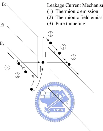
(26) described briefly as bellow.. 2-2-1. Leakage current. In AMLCD, TFTs play a switching device to turn ON/OFF the current path for charging/discharging the liquid crystal capacitor. Thus, the leakage current should be low enough to remain a pixel gray level before it must be refreshed. The leakage current mechanism in poly-Si has been studied by Olasupe [5]. The leakage current resulted from carrier generation from the poly-Si grain boundary defects. There are three major leakage mechanisms, as shown in Fig. 2-3. The dominant mechanism is a function of the prevailing drain bias. They pointed out carrier generation from grain boundary defects via thermionic emission and thermionic field emission to be prevalent at a low and medium drain biases, and carrier pure tunneling from poly-Si grain boundary defects to be the dominant mechanism at higher drain bias.. 2-2-2. Kink effect[6]. During devices operation, a high field near the drain could induce impact ionization there. Majority carriers, holes in the p-substrate for an n-channel poly-Si TFTs, generated by impact ionization will be stored in the substrate, since there is no substrate contact to drain away these charges. Therefore the substrate potential will be. 11.
(27) changed and will result in a reduction of the threshold voltage. This, in turn, may cause an increase or a kink in the current-voltage characteristics. The kink phenomenon is shown in Fig. 2-4. This float-body or kink effect is especially dramatic for n-channel devices, because of the higher impact-ionization rate of electrons. The kink effect can be eliminated by forming a substrate contact to the source of the transistor.. 12.
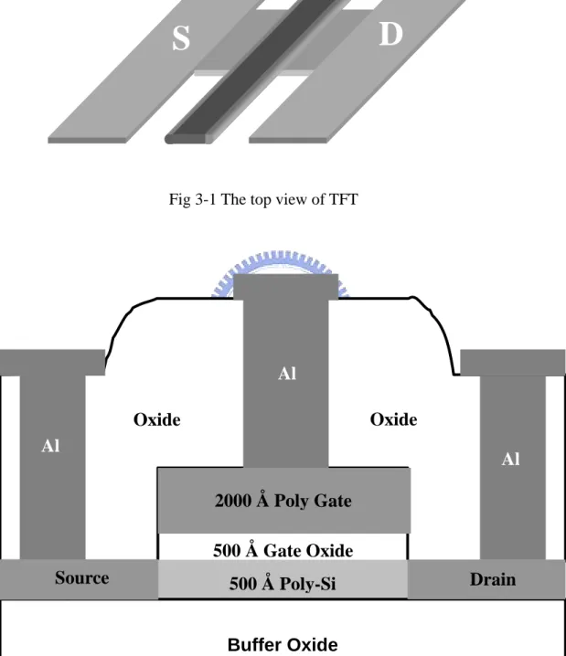
(28) Chapter 3 Experiment. 3-1. Fabrication Process of Poly-Si TFTs. In this thesis, the poly-Si TFTs with various Fluorine ion implantation doses were proposed and fabricated. The top view of the devices and the schematic cross section view of devices were shown in Fig. 3-1 and Fig. 3-2, respectively. The fabrication procedure is described as following.. Step1. Substrate. 6-inch 100-mm-thick p-type single-crystal silicon wafers with (100) orientation were used as the starting materials. After a standard cleaning procedure, silicon wafers were coated with 500-nm-thick thermally grown SiO2 in steam oxygen ambient at 1000ºC. In order to simulate the thin film transistor environment, the thick thermal oxide was grown on Si wafers.. Step2. Amorphous-Si thin film formation . Undoped amorphous-Si(a-Si) layers of thickness about 50-nm were deposited by. 13.
(29) low pressure chemical vapor deposition (LPCVD) on oxide by pyrolysis of silane (SiH4) at 550ºC. The transition temperature of Si material is about 575 ºC.. Step3. Fluorine ion implantation The fluorine ions implanted to the middle of the amorphous-Si layer without any pad oxide deposition first. The ion accelerating energy is 11 KeV and the doping dosages are 5x10¹³, 5x10¹⁴ and 5x1015 cm-2, respectively.. Step4-1. Poly-Si thin film formation (solid phase crystallization) . The amorphous-Si films were recrystallized by solid phase crystallization (SPC) method at 600ºC for 24hrs in N2 ambient. Then, the active regions were defined and etched. The etching was performed by dry etching by using transformer couple plasma (TCP) etching system.. Step4-2. Poly-Si thin film formation (excimer laser annealing) . The amorphous-Si films were recrystallized by excimer laser annealing (ELA) method at room temperature with an energy density of 300 mJ/cm2. Then, the active regions were defined and etched. The etching was performed by dry etching by using transformer couple plasma (TCP) etching system.. 14.
(30) Step5. Gate oxide formation. After defining the active region, the photoresist was removed by using O3 plasma etching and pure H2SO4 solution. The following step was to remove the polymer which was formed during the plasma etching. The remove for residue of polymer was realized by SC1 solution (NH4OH:H2O2:H2O=0.25:1:5). Before gate oxide deposition, the STD clean was used to clean the wafers. The HF dip was necessary to remove the native oxide at the poly-Si surface. Then, a 50nm layer of tetra-ethyl-ortho-silicate (TEOS) gate oxide was deposited by LPCVD at 7000C. The thickness of gate oxide was determined by N&K optical analyzer.. Step6. Gate electrode formation. After deposition of gate insulators, 200-nm-thick poly-silicon films were formed immediately on the gate insulators by LPCVD at 620°C. There was no any chemical solution clean between the deposition of TEOS oxide and poly-Si gate. The second poly-Si layer was then patterned by transformer couple plasma (TCP) etching to define the gate regions.. Step7. Source/drain formation. After the gate definition, source and drain regions were formed by phosphorous. 15.
(31) ions implantation. The ion accelerating energy is at 17 KeV and the dosage is 5x1015 cm-2.. Step8. Passivation layer and contact hole formation. The activation of source/drain regions was performed by the thermal budget of passivation layer deposition. The passivation layer was used TEOS oxide by LPCVD system. The duration and the temperature of passivation deposition were 3hrs and 700C, respectively. After the deposition of passivation layer, the activation was also finished. The passivation layer was 500-nm-thick to cap the poly-Si TFTs devices. The contact holes were patterned and then etched by buffer oxide etching (BOE) solution. The size of contact holes were 5x5 um2.. Step9. Metallization. The 500-nm aluminum layers were deposited by physical vapor deposition (PVD) and then patterned at the source, drain, and gate electrode as the metal pads. Finally, the devices were sintered at 350°C in hydrogen ambient for 30 min.. 16.
(32) 3-2. Measurement. In this thesis, the thickness of poly-Si, amorphous-Si, and TEOS oxide films were measured by N&K analyzer. The current-voltage characteristic measurement of thin film transistor devices was performed by KEITHLEY 4200 semiconductor parameter analyzer with source grounded and body floating.. 3-3. Methods of Device Parameter Extraction. In this section, we will introduce the methods of typical parameters extraction such as threshold voltage (VTH), subthreshold slope (S.S), drain current ON/OFF ratio (ION/IOFF), field-effect mobility (µFE) and the trap density (Nt) inside the channel.. 3-3-1. Determination of the threshold voltage Many methods are used to determinate the threshold voltage (VTH) which is the most important parameter required for TFT application. In poly-Si TFTs, the method used to determinate the threshold voltage is constant drain current method where the gate voltage at a specified drain current IN value is taken as the threshold voltage. This technique is adopted in most studies of TFTs. Typically, the threshold current IN = ID /. 17.
(33) (Weff / Leff ) is specified at 10 nA for VD = 0.1V (linear region) and 100 nA for VD = 5V (saturation region) in most papers to extract the threshold voltage of poly-Si TFTs.. 3-3-2. Determination of the subthreshold swing Subthreshold swing (V/dec.) is a typical parameter to describe the gate control ability of gate toward channel. It is defined as the amount of gate voltage required to increase/decrease drain current by one order of magnitude. The subthreshold swing should be independent of drain voltage and gate voltage. However, in reality, subthreshold swing might increase with drain voltage due to short-channel effects such as charge sharing, avalanche multiplication, and punchthrough-like effect. The subthreshold swing is also related to gate voltage due to undesirable factors such as serial resistance and interface state. In this experiment, the subthreshold swing is defined as the gate voltage required to decrease the threshold current by one orders of magnitude (from 10-9A to 10-10A).. 3-3-3. Determination of On/Off Current Ratio Drain On/Off current ratio is another important factor of TFTs. High On/Off ratio represents not only large turn-on current but also small off current (leakage current). It affects gray levels (the bright to dark state number) of TFT AMLCD directly.. 18.
(34) There are a lot of methods to specify the on and off current. In this experiment, the On current is equal to the maximum current, and the off current is defined as minimum leakage current while drain voltage is applied at 0.1V.. 3-3-4. Determination of the field-effect mobility The field-effect mobility (µFE) is determined from the transconductance (gm) at low drain voltage (VD=0.1V). The transfer I-V characteristics of poly-Si TFT can be expressed as. I D = µ FE C ox. W 1 2 [(VG − VTH )VD − VD ] L 2. (3-1). where Cox is the gate oxide capacitance per unit area, W is channel width, L is channel length, VTH is the threshold voltage. If VD is much smaller than VG-VTH ( i.e. VD << VG-VTH ) and VG > VTH, the drain current can be approximated as: I D = µ FE C ox. W (VG − VTH )VD L. (3-2). The transconductance is defined as. gm =. ∂I D ∂VG. VD = const .. =. WC ox µ FE VD L. (3-3) 19.
(35) Therefore, the field-effect mobility can be obtained by µ FE =. L gm C ox WV D. (3-4). 3-3-5. Determination of the poly-Si grain boundary trap density. As described in Eq. (2-3), the grain boundary potential barrier height VB is related to the carrier concentrations inside the grain and the trapping states located at grain boundaries. Based on this consideration, the amount of trap state density Nt can be extracted from the current-voltage characteristics of poly-Si TFTs. As proposed by Levinson et al[1], the I-V characteristics including the trap density can be obtained by :. I D = µ0Cox. q 3 Nt 2tch W (VG − VTH )VD exp(− ) 8kT ε s Cox (VG − VTH ) L. (3-5). This equation had been further corrected by Proano et al. by considering the mobility under low gate bias. It is found that the behavior of carrier mobility under low gate bias can be expressed more correctly by using the flat-band voltage VFB instead of the threshold voltage VTH. Moreover, a better approximation for channel thickness tch in an undoped material is given by defining the channel thickness as the thickness at which 80 percent of the total charge resides. Therefore, by solving the poisson’s equation, the channel thickness is given by :. 20.
(36) tch =. 8KT ε sε ox qCox (VG − VFB ). The drain current of TFTs should be expressed as. q 2 Nt 2 ε ox / ε s W I D = µ0Cox (VG − VFB )VD exp(− 2 ) L Cox (VG − VFB )2 The effective trap state density then can be obtained from the slope of the curve ln[ID/(VG-VFB)]versus(VG-VFB)-2.. 21.
(37) Chapter 4 Results and discussion. 4-1. Poly-Silicon Thin Film Transistor Fabricated by Solid Phase Crystallization (SPC) Method. 4-1-1. Device characteristic of poly-silicon TFTs Figure. 4-1 and Fig. 4-2 show typical transfer characteristics for various fluorine ion implantation dosages and standard poly-Si TFTs at VD=0.1V and VD=5V, respectively. Table I lists key parameters of poly-Si TFTs. Fig. 4-3 to 4-6 show the TFTs’ field effect mobility (µFE), threshold voltage (VTH), subthreshold swing (S.S) and ON/OFF ratio (Ion/Ioff) versus different fluorine ion implantation dosage. This result showed that the electrical characteristics could be improved for the fluorine ion implantation dosage was at 5x1013 cm-2. The field effect mobility increased from 19.74 to 54.48 cm2/volt-sec. The decreasing VTH, steep S.S and high On/Off ratio make it more potential for poly-Si TFTs application. As the implantation dosage increased to 5x1014cm-2, the electrical characteristics had a little degradation compared with 5x1013 cm-2 implanted devices, but it was still better than conventional poly-Si TFTs. When the implantation dosage was 5x1015 cm-2, the electrical. 22.
(38) characteristics were degraded seriously as shown in experimental result. It was found that the over amount of fluorine ion implantation doses caused the degraded electrical characteristics. The mechanism will be discussed in the following sections. The output characteristics of the fluorine implanted TFT and standard TFT are compared as shown in Fig. 4-7. It was found that the TFT with 5x1013 cm-2 implantation doses had the highest drain current in the same drain voltage, and drain current had degradation when the implantation dosage increased. This trend is the same as the transfer characteristics as shown in Fig. 4-1 and Fig. 4-2.. 4-1-2. The effects of fluorine passvation Figure. 4-8 shows the secondary-ion mass spectrometry (SIMS) depth profile of fluorine with different dosage. The depth profile showed a high concentration of fluorine near the poly-Si/oxide interface and surface. During the solid phase re-crystallization, the fluorine atoms segregated to the surface of poly-Si and the interface between poly-Si and oxide. It is believed that the surface-oxidized Si made the drive force for fluorine atoms segregated to the surface of poly-Si. Compared to the conventional fluorine ion incorporated poly-Si TFTs technology [1], the method we proposed needed no extra thermal annealing step and additional process steps. Figure.4-9 shows the trap state density with different Fluorine ion implantation. 23.
(39) dosages. It was known that the electrical characteristics of poly-Si TFTs, such as field effect mobility (µFE), threshold voltage (VTH), subthreshold swing (S.S) and ON/OFF ratio (Ion/Ioff), were affected by the trap state density [2-4]. The trap state density (Nt) of fluorine atoms incorporated poly-Si were various with the implantation dose in our experimental. As shown in Fig. 4-9, the implantation dosage of 5x1013cm-2 leaded to the decreased trap state density. We could calculate that the average fluorine concentration in poly-Si was about 1014cm-3(. 10 µ m ∗ 5 ∗1013 cm −2 ), which was enough 50nm. to passivate the defects in the poly-Si. As the implantation dose increasing, the trap state density increased. The over amount implantation doses caused even more trap state density than conventional poly-Si TFTs. It was reported that the fluorine atoms can break the stress induced strained bonds, likely the strained Si-O-Si bonds and Si-Si bonds to form stronger Si-F bonds, leading to local stress relaxation and thus decreasing the tail state density. Moreover, the fluorine atoms in the poly-Si channel can also passivate the dangling bonds to decrease deep state density [1], resulted in the subthreshold swing of the implanted device were improved. Fig.4-10 shows the scanning electron microscope (SEM) image of poly-Si grain with different fluorine dose after SPC method. It was found that the grain size didn’t vary obviously when the fluorine implantation dose was 5x1013cm-2 and 5x1014cm-2. However, the grain size decreased obviously when the implantation dose was 5x1015cm-2. This result. 24.
(40) showed that the higher concentration of fluorine atoms may hinder the grain growth, which caused increase of trap state density. In addition, the fluorine atoms behave as acceptors with their energy level in the valence band, and further shift the Fermi level toward the valence band [5]. This effect made the threshold voltage of 5x1014cm-2 implantation dosage become higher than that of standard TFT, which was different from the other parameter. Moreover, the over amount fluorine atoms might form the clusters [6], it also increased the trap states, resulted in the degradation of the electrical characteristics, such as µFE, Vth, S.S and Ion/Ioff in the experimental result. It was clear that the fluorine ions played two important roles in the poly-Si TFTs. One was the trap state density terminal, the other was the hole generator. In order to eliminate the trap state density, the over amount fluorine ions dosage was concerned. However, the extra trap states were generated to cause serious degraded electrical characteristics, resulted from the reduction of grain size and the formation of the clusters. From our experimental result, the appropriated fluorine ion implantation dose was 5x1013cm-2.. 4-1-3. The activation energy variation with fluorine incorporation. Fig. 4-11 shows the activation energy of drain current as a function of gate voltage measured at VD=5V for standard and fluorine ions implanted poly-Si TFTs.. 25.
(41) The activation energy was extracted by the measurement of ID-VG characteristic in the − Ea. temperature range from 20°C to 150°C. From the equation I D = I 0 e KT , using the linear fitting of the ln(ID) versus the 1/KT plot. Then the activation energy can be obtained. K is the Boltzmann constant and T is the temperature. In the preview research [7], the activation energy mean the carriers transportability which was related with the barrier height in the poly-Si channel. It was found that the activation energy was reduced for fluorine ions implanted poly-Si TFTs. It implied that the trap density eliminate by using fluorine ions implantation. This result is consistent with the above discussion.. 4-1-4. Stress result of poly-Si TFTs with/without fluorine implantation. The reliability for various fluorine ion dosage implanted poly-Si TFTs were also investigated in this study. Fig. 4-12 to 4-14 shows threshold voltage variation (△VTH ) , On current degradation and subthreshold swing variation (△S.S) versus stress time with/without fluorine implantation, and the stress condition was. VD=VG=20V. The stress time is 0, 100, 200, 600, 1000, 2000, 6000, 10000sec. It was found that the standard TFT showed serious degradation compared with the TFT with Fluorine implantation. Degradation of VTH, Ion and S.S is resulted from hot carrier multiplication near the drain side [8]. It was reported that the hot-carrier stress. 26.
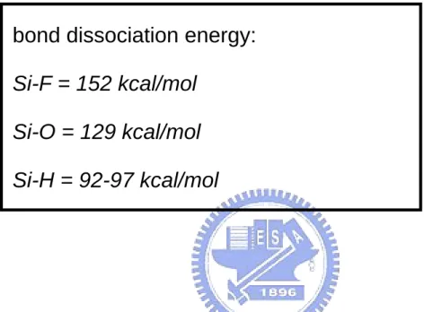
(42) induced degradation is attributed to the generation of gate-oxide/poly-Si interface states and/or the breaking of the Si-Si and/or Si-H weak bonds in the poly-Si channel [9-10]. Thus, the fluorine implanted into the channel with an appropriate dosage would result in the passivation of trap states and the formation of strong Si-F bonds in place of the weak Si-Si and Si-H bonds. The table Ⅱ shows the association energy of the different bonding. It is found the the Si-F bonds have the highest association energy, which lead to superior reliability of fluorine implanted poly-Si TFTs in comparison with TFTs without fluorine implantation.. 27.
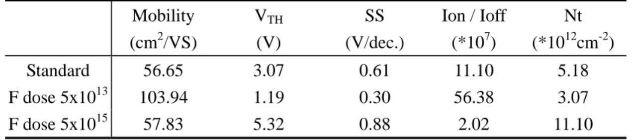
(43) 4-2. Poly-Silicon Thin Film Transistor Fabricated by Excimer Laser Annealing(ELA) Method. 4-2-1. Device characteristic of poly-silicon TFTs. Figure. 4-15 and 4-16 show typical transfer characteristics with various fluorine ion implantation dosages and standard poly-Si TFTs at VD=0.1V and VD=5V respectively. Table Ⅲ lists key parameters of poly-Si TFTs. Fig. 4-17 to 4-20 show the TFTs’ field effect mobility (µFE), threshold voltage (VTH), subthreshold swing (S.S) and ON/OFF ratio (Ion/Ioff) versus different fluorine ion implantation dosages. These result show that the electrical characteristics can be improved for the Fluorine ion implantation dosage is at 5x1013 cm-2, which have good agreement with the SPC poly-Si TFT. It was also found that the electrical characteristics were degraded seriously when the implantation dosage increased to 5x1015 cm-2. The output characteristics of the fluorine implanted TFT and standard TFT are compared as shown in Fig. 4-21. It was found that the TFT with implantation dosage of 5×1013cm-2 owned the largest drain current in this work. However, drain current was degraded when the implantation dosage increase. This trend is the same as the output characteristics of the SPC poly-Si TFTs as shown in Fig. 4-7.. 28.
(44) 4-2-2. The effects of fluorine passvation. Figure. 4-22 shows the secondary-ion mass spectrometry (SIMS) depth profile of fluorine with 5x1013 cm-2 dosages. The depth profile showed the same distribution as the SPC poly-Si TFTs. Fig. 4-23 shows the SEM result of poly-Si grain with different fluorine dose after ELA method. It was observed that the TFTs obtain the largest grain size with 5x1013 cm-2 fluorine doses. This result is different from solid phase crystallization (SPC) method. It was also observed that there were bubbles generated with 5x1015 cm-2 fluorine doses, resulted from the high temperature process during ELA. This result has a good agreement with the previous report [11-12]. Fig. 4-24 shows the trap state density (Nt) with different fluorine ion implantation dosages. It was found that the trap state density decreased obviously at implantation dosage 5x1013 cm-2, and the passivation effect of trap state density for ELA method was more excellent than SPC method in the experimental results. This might result from the grain size increases at 5x1013 cm-2 implantation doses for ELA method. Hence, the trap state density can be effectively eliminated for ELA poly-Si TFTs. However, it was found that the trap states increased with the implantation dosage, resulted from the the formation of the clusters and bubbles. This result was different as that of the SPC poly-Si TFTs.. 29.
(45) 4-2-3. The activation energy variation with fluorine incorporation. Fig. 4-25 shows the activation energy of drain current as a function of gate voltage measured at VD=5 V for standard and fluorine ion implanted poly-Si TFTs. the activation energy was extracted by the measurement of ID-VG characteristic in the temperature range from 20°C to 150°C. It was found that the activation energy was reduced for fluorine ions implanted poly-Si TFTs when the devices turn on. It implied that the trap density eliminate by using fluorine ions implantation which is the same as the result of the SPC TFT. However, In the off state we found that the activation energy of the fluorine ions implanted TFTs was lower than that of the standard TFTs, resulted from large leakage current as shown in Fig. 4-15.. 4-2-4. Stress result of poly-Si TFT with/without fluorine implantation. The reliability for various fluorine ion dosages implanted poly-Si TFTs were investigated in this study. Fig. 4-26 to 4-28 shows the threshold voltage variation (△VTH), On current degradation and subthreshold swing variation (△S.S) versus stress time with/without fluorine implantation, and the stress condition was. VD=VG=20V. It was found that the standard TFT shows serious degradation compared with the TFT with Fluorine implantation. The fluorine implanted into the channel. 30.
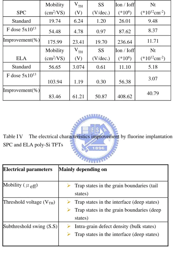
(46) would result in the formation of Si-F bonds. The Si-F bonds have the higher association energy, which lead to superior reliability of fluorine implanted poly-Si TFTs in comparison with TFTs without fluorine implantation.. 4-3. Comparison between SPC and ELA Poly-Silicon Thin Film Transistors. 4-3-1. Comparison of the electrical characteristics improvement. Table III shows the electrical characteristics improvement by fluorine implantation of SPC and ELA poly-Si TFTs. It was found that the SPC TFTs showed higher field effect mobility (µFE) improvement than that of ELA TFTs by fluorine incorporation. However, the ELA poly-Si TFTs revealed higher improvement in threshold voltage (VTH), subthreshold swing (S.S), ON/OFF ratio (Ion/Ioff) and trap state density (Nt). Table IⅤ shows the relation between the electrical parameter and the location of the trap states. It was found that the field effect mobility (µFE) is mainly affected by the amounts of tail states. Contrarily, threshold voltage (VTH) and subthreshold swing (S.S) is affected by the amounts of deep states. This result indicated that the fluorine passivation of tail states for SPC TFTs was more effective than that for ELA TFTs, and the ELA TFTs had higher passivation effect for deep trap. 31.
(47) states. It was also found that the ELA TFTs have lower trap states than SPC TFTs, resulted from the higher quality film formed by ELA method.. 4-3-2. Comparison of the reliability between ELA and SPC TFTs. Figure. 4-29 to 4-31 shows the threshold voltage variation (△VTH), On current degradation and subthreshold swing variation (△S.S) versus stress time of ELA and SPC TFT with/without fluorine implantation. It was found that the SPC TFTs showed better reliability than ELA TFTs. When the fluorine implanted, the improvement of On current degradation and subthreshold swing variation (△S.S) was almost the same between the SPC and ELA TFTs. However, the ELA TFTs showed smaller threshold voltage variation (△VTH) than SPC TFTs with fluorine implantation, which was different from the result of On current degradation and subthreshold swing variation (△S.S).. 32.
(48) Chapter 5 CONCLUSION. The fluorine ion implanted poly-Si TFTs were investigated in this study. The implantation dosage affected the electrical characteristics of the poly-Si TFTs. We found that as the implantation dose is 5x1013cm-2, the device has the lowest trap state density, result in the superior characteristics, such as a higher mobility, a lower threshold voltage, a steep subthreshold swing and high On/Off ratio. It is believed that the fluorine atoms can break the stress induced strained bonds, likely the strained Si-O-Si bonds and Si-Si bonds to form stronger Si-F bonds, leading to local stress relaxation and thus decreasing the tail state density. Moreover, the fluorine atoms in the poly-Si channel can also passivate the dangling bonds to decrease deep state density. In addition, the Si-F bonds is stronger, result in the improved reliability compared to conventional TFT. The electrical characteristic will be degraded as the fluorine ion implantation dosage is over-increasing, result from the formation of the cluster. The directly re-crystallized method made the fluorine atoms segregated in the poly-Si/gate oxide interface which reduced the process step compared to conventional fluorine ion implantation investigation. The fluorine ion implantation is consisted with the conventional poly-Si TFTs process flow and the process is uncomplicated. 33.
(49) References. Chapter 1 [1.1]. H. Oshima and S. Morozumi, “Future trends for TFT integrated circuits on glass substrates,” IEDM Tech. Dig., 157 (1989). [1.2] M. Stewart, R. S. Howell, L. Pires, and M. K. Hatalis, “Polysilicon TFT technology for active matrix OLED displays ,” IEEE Trans. Electron Devices, vol. 48, pp. 845-851, 2001 [1.3]. H. Kuriyama et al., “An asymmetric memory cell using a C-TFT for ULSI SRAM,” Symp. On VLSI Tech., p.38, 1992. [1.4]. T. Yamanaka, T. Hashimoto, N. Hasegawa, T. Tanala, N. Hashimoto, A. Shimizu, N. Ohki, K. Ishibashi, K. Sasaki, T. Nishida, T. Mine, E. Takeda, and T. Nagano, “Advanced TFT SRAM cell technology using a phase-shift lithography,” IEEE Trans. Electron Devices, Vol. 42, pp.1305-1313,1995.. [1.5]. K. Yoshizaki, H. Takaashi, Y. Kamigaki, T.asui, K. Komori, and H. Katto, ISSCC Digest of Tech., p.166, 1985. [1.6]. N. D.Young, G. Harkin, R. M. Bunn, D. J. McCulloch, and I. D. French , “The fabrication and characterization of EEPROM arrays on glass using a low-temperature poly-Si TFT process,” IEEE Trans. Electron Devices, Vol. 43, pp. 1930-1936, 1996.. [1.7]. T. Kaneko, U. Hosokawa, N. Tadauchi, Y. Kita, and H. Andoh, “400 dpi integrated contact type linear image sensors with poly-Si TFT's analog readout circuits and dynamic shift registers,” IEEE Trans. Electron Devices, Vol. 38, pp. 1086-1093, 1991. [1.8]. U. Hayashi, H. Hayashi, M. Negishi, T. Matsushita, Proc. of IEEE Solid-State Circuits Conference (ISSCC), p. 266 , 1998.. [1.9]. N.Yamauchi, U. Inava, and M. Okamura, “An integrated photodetector34.
(50) amplifier using a-Si p-i-n photodiodes and poly-Si thin-film transistors,” IEEE Photonic Tech. Lett, Vol. 5, pp. 319-321, 1993. [1.10]. M. G. Clark, IEE Proc. Circuits Devices Syst, Vol. 141, 133 (1994). [1.11] Noriyoshi Yamauchi, Jean-Jacques J. Hajjar and Rafael Reif, “Polysilicon Thin-Film Transistors with Channel Length and Width Comparable to or Smaller than the Grain Size of the Thin Film,” IEEE Trans. Electron Devices, Vol. 38, pp 55-60, 1991 [1.12]. Singh Jagar, Mansun Chan, M. C. Poon, Hongmei Wang, Ming Qin, Ping K. Ko, Yangyuan Wang, “Single Grain Thin-Film-Transistor (TFT) with SOI CMOS Performance Formed by Metal-Induced-Lateral-Crystallization,” IEDM Tech. Dig., pp. 293-296, 1999.. [1.13]. K. Nakazawa, “Recrystallization of amorphous silicon films deposited by low-pressure chemical vapor deposition from Si2H6 gas,” J. Appl. Phys, Vol. 69, pp. 1703-1706, 1991.. [1.14]. T. J. King and K. C. Saraswat, “Low-temperature fabrication of poly-Si thin-film transistors,” IEEE Electron Device Lett, Vol. 13, pp. 309-311, 1992.. [1.15]. H. Kuriyama, S. Kiyama, S. Noguchi, T. Kuahara, S. Ishida, T. Nohda, K. Sano, H. Iwata, S. Tsuda, and S. Nakano, “High mobility poly-Si TFT by a new excimer laser annealing method for large area electronics,” IEDM Tech. Dig, Vol. 91, p. 563, 1991. [1.16]. S. W. Lee and S. K. Joo, “Low temperature poly-Si thin-film transistor fabricated by metal-induced lateral crystallization,” IEEE Electron Device Lett., vol. 17, p. 160, 1996.. [1.17]. J. Levinson, F. R. Shepherd, P. J. Scanlon, W. D. Westwood, G. Este, and M. Rider, “Conductivity behavior in polycrystalline semiconductor thin film transistors,” J. Appl. Phys. Vol. 53, pp.1193-1202, 1982. [1.18] P. Migliorato, C. Reita, G. Tallatida, M. Quinn and G. Fortunato, “Anomalous. 35.
(51) off-current mechanisms in n-channel poly-Si thin film transistors.” Solid-State-Electronics, Vol.38, pp.2075-2079, 1995 [1.19]. M. Hack, I-W. Wu, T. H. King and A. G. Lewis, “Analysis of Leakage Currents in Poly-silicon Thin Film Transistors,” IEDM Tech. Dig., vol. 93, pp. 385-387, 1993. [1.20]. N. D. Young, G. Harkin, R. M. Bunn, D. J. McCulloch, and I. D. French, “The fabrication and characterization of EEPROM arrays on glass using a low-temperature poly-Si TFT process,” IEEE Trans. Electron Devices, Vol. 43, No. 11, pp. 1930-1936, 1996.. [1.21]. K. Ono, T. Anoyama, N. Konishi, and K. Miyata, “Analysis of current-voltage characteristics of low-temperature-processed polysilicon thin-film transistors, ” IEEE Trans. Electron. Device,. Vol.39, no.5, p.792,. 1992. [1.22] M Hack, I. W. Wu, T. J. King, and A. G. Lewis, “Analysis of leakage currents in poly-silicon thin-film transistors, ” IEEE IEDM Tech. Dig., 1993, p385. [1.23]. A. Rodriguez, E.G. Moreno, H. Pattynn, J. F. Nijis, and R. P. Mertens, “Model for the anomalous off current of polysilicon thin film transistors and diodes,” IEEE Trans. Electron Devices, Vol.40, no.5, p.938, 1993.. [1.24]. I. W. Wu, A. G. Lewis, T. Y. Huang, W. B. Jackson, and A. Chiang, “Mechanism and device-to-device variation of leakage current in polysilicon thin film transistors, ” IEEE IEDM tech. Dig., 1990, p.867.. [1.25]. T. I. Kamins and Marcoux, “hydrogenation of transistors fabricated in polycrystalline-silicon films, ” IEEE Electron Device Lett., Vol.1, no.8, p.159, 1980. [1.26]. A. Yin and S. J. Fonash, “High-performance p-channel poly-Si TFTs using electron cyclotron resonance hydrogen plasma passivation, ” IEEE Electron Device Lett., Vol.15, no.12, p.502, 1994.. 36.
(52) [1.27] M. Hack, A. G. Lewis, and I. W. Wu, “Physical models for degradation effects in polysilicon thin film transistors, ” IEEE Trans. Electron Devices, Vol.40, no.5, p.890, 1993. [1.28]. A. G. Lewis, I. W. Wu, M. Hack,, A. Chiang, and R. H. Bruce, “Degradation of polysilicon TFTs during dynamic stress, ”IEEE IEDM Tech. Dig., p.575, 1991.. [1.29]. H. N. Chern, C. L. Lee, and T. F. Lei, “The effects of fluorine passivation on polysilicon thin-film transistors,” IEEE Transaction on electron devices., Vol.41, .p.698, 1994. [1.30]. J. W. Park, B. T. Ahn and K. Lee, “Effects of F+ implantation on the characteristics of poly-Su films and low-temperature n-ch poly-Si thin-film transistors, ”Jan. J. Appl. Phy. Vol.34, p.1436, 1995. [1.31]. Shigeto Maegawa, Takashi Ipposhi, Shigenobu Maeda, Hisayuki Nishimura, Tsutomu Ichiki, Motoi Ashida, Osamu Tanina, Yasuo Inoue, Tadashi Nishimura, Member, IEEE and Natsuro Tsubouchi, “Performance and reliability improvements in poly-Si TFT’s by fluorine implantation into gate poly-Si, ” IEEE Trans. Electron Devices, Vol.42, no.6, 1995.. Chapter 2. [2.1]. J. Levinson, F. R. Shepherd, P. J. Scanlon, W. D. Westwood, G. Este, and M. Rider, “Conductivity behavior in polycrystalline semiconductor thin film transistors,” J. Appl. Phys. Vol. 53, pp.1193-1202, 1982. [2.2]. P. Migliorato, C. Reita, G. Tallatida, M. Quinn and G. Fortunato, “Anomalous off-current mechanisms in n-channel poly-Si thin film transistors.” Solid-State-Electronics, Vol.38, pp.2075-2079, 1995. [2.3]. M. Hack, I-W. Wu, T. H. King and A. G. Lewis, “Analysis of Leakage Currents in Poly-silicon Thin Film Transistors,” IEDM Tech. Dig., vol. 93, pp. 37.
(53) 385-387, 1993 [2.4]. “Polycrystalline silicon for integrated circuits and displays”, second edition, written by Ted Kamins, pp.200-210.. [2.5]. K. R. Olasupo and M. K. Hatalis, “ Leakage Current Mechanism in Sub-Micron Polysilicon Thin-Film Transistors ”IEEE Trans. Electron Devices, Vol. 43, pp.1218, (1996).. [2.6]. “Semiconductor devices physics and technology” , second edition, written by S.M Sze, pp. 199-213. Chapter 3. [3.1]. J. Levinson, F.R. Shepherd, P.J. Scanlon, W.D. Westwood, G. Este, and M. Rider, “ Conductivity behavior in polycrystalline semiconductor thin film transistors” J. Appl. Phys, pp.1193-1202, 1981. Chapter 4. [4.1]. H. N. Chern, C. L. Lee, and T. F. Lei, “The effects of fluorine passivation on polysilicon thin-film transistors,” IEEE Transaction on electron devices., Vol.41, .p.698, 1994.. [4.2]. J. Levinson, F. R. Shepherd, P. J. Scanlon, W. D. Westwood, G. Este, and M. Rider, “Conductivity behavior in polycrystalline semiconductor thin film transistors, ” J. Appl. Phys. Vol.53, p.1193-1202, 1982.. [4.3]. P. Migliorato, C. Reita, G. Tallatida, M. Quinn and G. Fortunato, “Anomalous off-current. mechanisms. in. n-channel. poly-Si. thin. film. transistors, ”Solid-State-Electronics, Vol.38, p.2075-2079, 1995. [4.4]. M. Hack, I-W. Wu, T. H. King and A. G. Lewis, “Analysis of Leakage Currents 38.
(54) in Poly-silicon Thin Film Transistors,” IEDM Tech. Dig., vol. 93, pp. 385-387, 1993 [4.5]. Cs. Szeles, B. Nielsen, P, Asoka-Kumar, and K. G. Lynn, “Role of implantation-indeced defects in surface-oriented diffusion of fluorine in silicon. ”J. Appl. Phys, Vol.76, 15 September 1994.. [4.6]. Harry J Whitlow, Juhani Keinonen, Carina Zaring and C Sture Petersson, “Thermal. redistribution. of. fluorine. in. BF2+-implanted. SiO2/Si. structures. ”Semicond. Sci. Technol. Vol2, 1987. [4.7]. Ching-Lin Fan and Mao-Chieh Chen, “Performance Improvement of Excimer Laser. Annealed. Poly-Si. TFTs. Using. Fluorine. Ion. Implantation,”. Electrochemical and Solid-State Letters, Vol.5, p.75-77, 2002. [4.8] I.W. Wu, T.Y. Huang, Warren B. Jackson, Alan G. Lewis, and Anne Chiang, “Passivation kinetics of two types of defects in polysilicon TFT by plasma hydrogenation,” IEEE Electron Device Letter., Vol.12, p.181, 1991. [4.9]. S. Banerjee, R. Sundaresan, H. Shichijo, and S. Malhi, “Hot-electron degradation of n-channel polysilicon MOSFETs,” IEEE Trans. Electron Devices, Vol.35, p.152 , 1988.. [4.10]. M. Hack, A. G. Lewis, and I. W. Wu, “Physical models for degradation effects in polysilicon thin film transistors, ” IEEE Trans. Electron Devices, Vol.40, no.5, p.890, 1993. [4.11] C. W. Nieh and L. J. Chen, “Formation of bubbles in BF2+-implanted silicon, ”Appl. Phys Lett. Vol.48, No.22, 1986. [4.12] C. W. Nieh and L. J. Chen, “Cross-sectional transmission electron microscope study of residual defects in BF2+-implanted (001)Si, ”J. Appl. Phys. Vol.60, 1986.. 39.
(55) Fig. 2-1 Sketch of the band diagram of the polycrystalline silicon films. Vg Z Y. W. Vd. Gate. X. Gate oxide. t. Source N+. Drain. N+. L. 0. Fig. 2-2 A schematic MOSFET cross section, showing the axes of coordinates and the bias voltages at the four terminals for the drain-current model.. 40.
(56) Ec. Leakage Current Mechanism (1) Thermionic emission (2) Thermionic field emission (3) Pure tunneling. Et. 1 Ev. 2 3 3 2. 1. Fig. 2-3 Three possible mechanisms of leakage current in poly-Si TFTs, including thermionic emission, thermionic field emission and pure tunneling. 41.
(57) Fig. 2-4 The kink effect in the output characteristics of an n-channel SOI MOSFET[6]. 42.
(58) G. D. S. Fig 3-1 The top view of TFT. Al Oxide Oxide. Oxide Al. Al 2000 Å Poly Gate 500 Å Gate Oxide. Source. 500 Å Poly-Si Buffer Oxide. Fig 3-2 Cross-section view of TFT. 43. Drain.
(59) 10-4 10-5. Drain Current ID(A). 10-6. W/L=10μm/10μm. 10-7 10-8 10-9 10-10 10-11. Standard F dose 5x1013 cm-2 F dose 5x1014 cm-2 F dose 5x1015 cm-2. 10-12 10-13 10-14 -5. 0. 5. 10. 15. 20. Gate Voltage VG(V). Fig.4-1 Transfer characteristic for fluorine implanted SPC TFT and standard SPC TFT at VD=0.1V. 44.
(60) 10-3. Drain Current ID(A). 10-4. W/L=10μm/10μm. 10-5 10-6 10-7 10-8. Standard F dose 5x1013 cm-2 F dose 5x1014 cm-2 F dose 5x1015 cm-2. 10-9 10-10 10-11 -5. 0. 5. 10. 15. 20. Gate Voltage VG(V). Fig.4-2 Transfer characteristic for fluorine implanted SPC TFT and standard SPC TFT at VD=5V. 45.
(61) Standard F dose 5x10¹³ F dose 5x10¹⁴ F dose 5x10¹⁵. Mobility (cm2/VS). VTH (V). SS (V/dec.). Ion / Ioff (*106). Nt (*1012cm-2). 19.74 54.48 48.12 15.17. 6.24 4.78 6.69 10.36. 1.20 0.97 1.13 1.62. 26.01 87.62 67.31 1.94. 9.48 8.37 9.17 10.90. Table I Device parameters for standard SPC TFT and fluorine implanted SPC TFT, including mobility, threshold voltage(VTH), subthreshold swing(S.S), Ion/Ioff ratio and trap state density(Nt). All parameters were extracted at VD=0.1V. 46.
(62) 50. 2. -1 -1. Field Effect Mobility (cm V s ). 60. 40. 30. 20. 10 standard. 5e+13. 5e+14. 5e+15. Fluorine Implantation Dosage Fig.4-3 Field effect mobility (µFE) versus different fluorine implantation dosage SPC poly-Si TFTs.. Threshold Voltage Vth (V). 11 10 9 8 7 6 5 4 standard. 5e+13. 5e+14. 5e+15. Fluorine Implantation Dosage Fig.4-4 Threshold voltage (VTH) versus different fluorine implantation dosage SPC poly-Si TFTs. 47.
(63) Subthreshold Swing S.S (V/dec). 1.7 1.6 1.5 1.4 1.3 1.2 1.1 1.0 0.9 standard. 5e+13. 5e+14. 5e+15. Fluorine Implantation Dosage Fig.4-5 Subthreshold swing (S.S) versus different fluorine implantation dosage SPC poly-Si TFTs.. 10. 7. Ion/Ioff Ratio (*10 ). 8 6 4 2 0. standard. 5e+13. 5e+14. 5e+15. Fluorine Implantation Dosage Fig.4-6 Ion/Ioff ratio versus different fluorine implantation dosage SPC poly-Si TFTs.. 48.
(64) W/L=10μm/10μm Vg=4V, 7V, 10V 160. Standard F dose 5x1013 cm-2 F dose 5x1014 cm-2 F dose 5x1015 cm-2. Drain Current ID(µΑ). 140 120 100 80 60 40 20 0 0. 2. 4. 6. 8. 10. 12. Drain Voltage VD(V). Fig.4-7 Output characteristic for fluorine implanted SPC TFT and standard SPC TFT.. 49.
(65) Concentration (atoms/cc). 1022 1021 1020 1019 1018 F 5x1015 cm-2 F 5x1014 cm-2. 1017 1016. F 5x1013 cm-2. 1015. poly-Si channel. buffer oxide. 1014 0. 10. 20. 30. 40. 50. 60. 70. 80. 90. 100. Depth (nm). Fig.4-8 Secondary-ion mass spectrometry (SIMS) depth profile with various fluorine ion implantation doses after solid phase re-crysatllization(600℃ for 24 hrs).. 50.
(66) -2. Trap State Density Nt (*10 cm ). 11.5. 12. 11.0 10.5 10.0 9.5 9.0 8.5 8.0 standard. 5e+13. 5e+14. 5e+15. Fluorine Implantation Dosage. Fig.4-9 Trap state density (Nt) versus different fluorine implantation dosage SPC poly-Si TFTs.. 51.
(67) STD. F-5E13. F-5E14. F-5E15. Fig.4-10 The scanning electron microscope (SEM) image of poly-Si grain with different fluorine doses after SPC method.. 52.
(68) 0.8 standard F dose 5x1013cm-2. Active Energy Ea(eV). 0.6 0.4 0.2 0.0 VD=5V. -0.2 -0.4 -5. 0. 5. 10. 15. Gate Voltage VG(V). Fig.4-11 The activation energy of drain current as a function of gate voltage measured at VD=5 V for standard and fluorine ion implanted SPC poly-Si TFTs. 53.
(69) Threshold voltage variation ∆Vth(V). 6 Stress condition VD=VG=20V. 5 4. standard F dose 5x1013cm-2. 3 2 1 0 ion1Vd=Vg=10V102 100Stress condit10. 103. 104. stress time(sec). Fig.4-12 Threshold voltage variation (ΔVTH) of SPC poly-Si TFTs with/without fluorine implantation versus stress time under a stress voltage VD=VG=20V.. 54.
(70) 0.0 Stress condition VD=VG=20V. ∆Ion/Ion. -0.2 -0.4 -0.6 standard. -0.8. F dose 5x1013cm-2. -1.0 100. 101. 102. 103. 104. stress time (sec). Fig.4-13 On-current degradation of SPC poly-Si TFTs with/without fluorine implantation versus stress time under a stress voltage VD=VG=20V.. 55.
(71) Subthreshold swing variation (∆S.S). 2.5 standard. 2.0. F dose 5x1013cm-2. 1.5 1.0 0.5 Stress condition VD=VG=20V. 0.0 100. 101. 102. 103. 104. stress time (sec). Fig.4-14 Subthreshold swing variation (ΔS.S) of SPC poly-Si TFTs with/without fluorine implantation versus stress time under a stress voltage VD=VG=20V.. 56.
(72) bond dissociation energy: Si-F = 152 kcal/mol Si-O = 129 kcal/mol Si-H = 92-97 kcal/mol. Table Ⅱ The association energy of the different bonding. 57.
(73) 10-4 10-5. W/L=10μm/10μm. Drain Current ID(A). 10-6 10-7 10-8 10-9 10-10 10. standard 13. -2. F dose 5x10 cm 15 -2 F dose 5x10 cm. -11. 10-12 10-13 10-14 -5. 0. 5. 10. 15. 20. Gate Voltage VG(V). Fig.4-15 Transfer characteristic for fluorine implanted ELA TFT and standard ELA TFT at VD=0.1V. 58.
(74) 10-3. Drain Current Id(A). 10-4. W/L=10μm/10μm. 10-5 10-6 10-7 10-8. Standard F dose 5x1013 cm-2 F dose 5x1015 cm-2. 10-9 10-10 10-11 -10. -5. 0. 5. 10. 15. 20. Gate Voltage Vg(V). Fig.4-16 Transfer characteristic for fluorine implanted ELA TFT and standard ELA TFT at VD=5V. 59.
(75) Standard F dose 5x10¹³ F dose 5x10¹⁵. Mobility (cm2/VS). VTH (V). SS (V/dec.). Ion / Ioff (*107). Nt (*1012cm-2). 56.65 103.94 57.83. 3.07 1.19 5.32. 0.61 0.30 0.88. 11.10 56.38 2.02. 5.18 3.07 11.10. Table Ⅲ Device parameters for standard ELA TFT and fluorine implanted ELA TFT, including mobility, threshold voltage(VTH), subthreshold swing(S.S), Ion/Ioff ratio and trap state density(Nt). All parameters were extracted at VD=0.1V. 60.
(76) 100. 2. -1 -1. Field Effect Mobility (cm V s ). 110. 90 80 70 60 50 standard. 5e+13. 5e+15. Fluorine Implantation Dosage Fig.4-17 Field effect mobility (µFE) versus different fluorine implantation dosage ELA poly-Si TFTs.. Threshold Voltage Vth (V). 6 5 4 3 2 1 0 standard. 5e+13. 5e+15. Fluorine Implantation Dosage Fig.4-18 Threshold voltage (VTH) versus different fluorine implantation dosage ELA poly-Si TFTs. 61.
(77) Subthreshold Swing S.S (V/dec). 1.0 0.9 0.8 0.7 0.6 0.5 0.4 0.3 0.2 standard. 5e+13. 5e+15. Fluorine Implantation Dosage Fig.4-19 Subthreshold swing (S.S) versus different fluorine implantation dosage ELA poly-Si TFTs.. 60. 7. Ion/Ioff Ratio (*10 ). 50 40 30 20 10 0 standard. 5e+13. 5e+15. Fluorine Implantation Dosage Fig.4-20 Ion/Ioff ratio versus different fluorine implantation dosage ELA poly-Si TFTs. 62.
(78) W/L=10μm/10μm Vg=4V, 7V, 10V 300. Standard F dose 5x1013 cm-2 F dose 5x1015 cm-2. Drain Current ID(µΑ). 250 200 150 100 50 0 0. 2. 4. 6. 8. 10. 12. Drain Voltage VD(V). Fig.4-21 Output characteristic for fluorine implanted ELA TFT and standard ELA TFT.. 63.
(79) 1021 Concentration ( atoms/c.c ). F 5x1015 cm-2. 1020 1019 1018 1017 Poly-Si. Buffer Oxide. 1016 0. 20. 40. 60. 80. 100. 120. 140. Depth ( nm ). Fig.4-22 Secondary-ion mass spectrometry (SIMS) depth profile with 5x1013 cm-2 fluorine ion implantation doses after excimer laser re-crysatllization.. 64.
(80) STD. F-5E14. F-5E13. F-5E15. Fig.4-23 The scanning electron microscope (SEM) image of poly-Si grain with different fluorine doses after ELA method. The grain with the 5x1013 cm-2 fluorine ion implantation doses was the largest, and the other grains almost had the same size.. 65.
(81) 12. -2. Trap State Density Nt (*10 cm ). 12. 10. 8. 6. 4. 2 standard. 5e+13. 5e+15. Fluorine Implantation Dosage. Fig.4-24 Trap state density (Nt) versus different fluorine implantation dosage ELA poly-Si TFTs.. 66.
(82) 0.8 standard F dose 5x1013cm-2. Active Energy Ea(eV). 0.6 0.4 0.2 0.0 VD=5V -0.2 -0.4 -5. 0. 5. 10. 15. Gate Voltage VG(V). Fig.4-25 The activation energy of drain current as a function of gate voltage measured at VD=5V for standard and fluorine ion implanted ELA poly-Si TFTs. 67.
(83) Threshold voltage variation ∆Vth(V). 6 Stress condition VD=VG=20V. 5 4. standard 13 -2 F dose 5x10 cm Stress condition VD=VG=20V. 3 2 1 0 100. 101. 102. 103. 104. stress time (sec). Fig.4-26 Threshold voltage variation (ΔVth) of poly-Si ELA TFTs with/without fluorine implantation versus stress time under a stress voltage VD=VG=20V.. 68.
(84) Stress condition VD=VG=20V. 0.0. ∆Ion/Ion. -0.2. Stress condition VD=VG=20V. -0.4 -0.6 -0.8 -1.0 -1.2 100. standard F dose 5x1013cm-2. 101. 102. 103. 104. stress time (sec). Fig.4-27 On-current degradation of ELA poly-Si TFTs with/without fluorine implantation versus stress time under a stress voltage Vd=Vg=20V.. 69.
(85) Subthreshold swing variation (∆S.S). 3.5 Stress condition VD=VG=20V. 3.0 2.5 2.0 standard. 1.5. F dose 5x1013cm-2. 1.0 0.5 0.0 100. 101. 102. 103. 104. stress time (sec). Fig.4-28 Subthreshold swing variation (ΔS.S) of ELA poly-Si TFTs with/without fluorine implantation versus stress time under a stress voltage VD=VG=20V.. 70.
(86) Mobility. VTH. SPC. (cm2/VS). Standard. Ion / Ioff. Nt. (V). SS (V/dec.). (*106). (*1012cm-2). 19.74. 6.24. 1.20. 26.01. 9.48. F dose 5x10¹³. 54.48. 4.78. 0.97. 87.62. 8.37. Improvement(%). 175.99. 23.41 VTH. 19.70. 236.64. 11.71. Ion / Ioff. Nt. (*10 ). (*1012cm-2) 5.18. ELA. 2. (cm /VS). (V). SS (V/dec.). Standard. 56.65. 3.074. 0.61. 11.10. 103.94. 1.19. 0.30. 56.38. 83.46. 61.21. 50.87. 408.62. Mobility. 6. F dose 5x10¹³ Improvement(%). 3.07 40.79. Table IⅤ The electrical characteristics improvement by fluorine implantation of SPC and ELA poly-Si TFTs. Electrical parameters. Mainly depending on. Mobility (μeff). ¾ Trap states in the grain boundaries (tail states). Threshold voltage (VTH). ¾ Trap states in the interface (deep states) ¾ Trap states in the grain boundaries (deep states). Subthreshold swing (S.S). Table Ⅴ. ¾ Intra-grain defect density (bulk states) ¾ Trap states in the interface (deep states). The relation between the electrical parameter and the location of the trap. states.. 71.
(87) Threshold voltage variation ∆Vth(V). 6 5 4. standard(ELA) 13 -2 F dose 5x10 cm (ELA) standard(SPC) F dose 5x1013cm-2(SPC). 3 2 1 0 100. 101. 102. 103. 104. stress time (sec). Fig.4-29 Threshold voltage variation (ΔVth) of ELA and SPC poly-Si TFTs with/without fluorine implantation versus stress time under a stress voltage VD=VG=20V.. 72.
(88) 0.0. ∆Ion/Ion. -0.2 -0.4 -0.6 -0.8 -1.0 -1.2 100. standard(ELA) 13 -2 F dose 5x10 cm (ELA) standard(SPC) 13 -2 F dose 5x10 cm (SPC). 101. 102. 103. 104. stress time (sec). Fig.4-30 On-current degradation of ELA and SPC poly-Si TFTs with/without fluorine implantation versus stress time under a stress voltage VD=VG=20V.. 73.
(89) Subthreshold swing variation (∆S.S). 3.5 3.0 2.5 2.0 1.5 standard(ELA) F dose 5x1013cm-2(ELA) standard(SPC) 13 -2 F dose 5x10 cm (SPC). 1.0 0.5 0.0 100. 101. 102. 103. 104. stress time(sec). Fig.4-31 Subthreshold swing variation (ΔS.S) of ELA and SPC poly-Si TFTs with/without fluorine implantation versus stress time under a stress voltage VD=VG=20V.. 74.
數據
![Fig. 2-4 The kink effect in the output characteristics of an n-channel SOI MOSFET [6]](https://thumb-ap.123doks.com/thumbv2/9libinfo/8555351.188321/57.892.230.639.314.717/fig-kink-effect-output-characteristics-channel-soi-mosfet.webp)
+4
Outline
相關文件
在1980年代,非晶矽是唯一商業化的薄膜型太 陽能電池材料。非晶矽的優點在於對於可見光
3 The teaching modes of ELA in English include collaboration between non-language subject teachers and English Language teachers to conduct cross-curricular English
雙極性接面電晶體(bipolar junction transistor, BJT) 場效電晶體(field effect transistor, FET).
PIV: parainfluenza virus, RSV: respiratory syncytial virus, MPV: metapneumovirus, Group A Strept: group A streptococcal disease.. Rhinovirus 鼻病毒
1、 Focusing on the unit of “circle”, the variation of the learning achievement between the experimental group and the control group reached significant difference3. The variation
Regardless of the assumed copula functions, we consistently find that the Chinese market experiences not only a higher degree of dependence but also a higher variation of
Umezaki,B., Tamaki and Takahashi,S., "Automatic Stress Analysis of Photoelastic Experiment by Use of Image Processing", Experimental Techniques, Vol.30 , P22-27,
In different gender、time for study、time for cram、the parents education level and household income of junior high school students , some aspects of the academic stress were
