國
立
交
通
大
學
電子工程學系 電子研究所碩士班
碩 士 論 文
以氧化鉿為介電層的電阻式記憶體之電性與分析
Electrical characteristics and analyses of HfOx
based resistive random access memorie
s
研 究 生:王佳文
指導教授:林鴻志 博士
黃調元 博士
以氧化鉿為介電層的電阻式記憶體之電性與分
析
Electrical characteristics and analyses of HfOx
based resistive random access memorie
s
研 究 生:王佳文 Student :Chia-Wen Wang
指導教授:林鴻志 博士 Advisors:Dr. Horng-Chih Lin
黃調元 博士
Dr. Tiao-Yuan Huang
國 立 交 通 大 學
電子工程學系 電子研究所碩士班
碩 士 論 文
Submitted to Department of Electronics Engineering & Institute of Electronics College of Electrical Engineering and Computer Engineering
National Chiao Tung University in Partial Fulfillment of the Requirements
for the Degree of Master of Science
in
Electronics Engineering July 2013
Hsinchu, Taiwan, Republic of China
i
以氧化鉿為介電層的電阻式記憶體之電性與分
析
研究生:王佳文
指導教授: 林鴻志 博士 黃調元 博士 國立交通大學 電子工程學系 電子研究所碩士班摘要
在本篇論文中,我們探討以氧化鉿為介電層的電阻式記憶體的電性。首先 我們製備有著不同氧化鉿厚度的 Ni/HfOx/TiN 以及 TiN/Ti/HfOx/TiN RRAM 元件, 並且量測在不同限流(compliance current)以及 reset 時施加不同大小偏壓對元件電 性的影響。接著我們探討不同厚度的鈦緩衝層對元件造成的影響。此外,為了瞭 解造成 overshoot current 的根源,我們利用外接 1T1R 的量測配置來量測 Ni/HfOx/TiN RRAM 元件的 電性。 而為 了 探討電 流的傳 導機 制 以及傳 導絲 (conductive filament)的性質,我們進行了電流-電壓關係曲線的擬和(fitting)以及變 溫量測。 我們觀察到限流的大小對於低組態的電阻有著相當大的影響,並且我們也 觀察到在 reset 時施加不同大小偏壓會影響高組態的電阻以及之後 set 所需要施加 的偏壓大小。這指出一個 RRAM 元件的電流開關比(on/off ratio)以及操作功率 (operation power)是可調變而非定值的。另一方面,在 RRAM 元件中置入鈦緩衝ii 層對 forming 所需要施加的偏壓有著相當大的影響,也因此為了使元件有穩定的 切換特性,鈦緩衝層以及氧化鉿的厚度是需要被優化的。此外,使用外接 1T1R 的量測配置去進行量測還是觀察到了 overshoot current,這表示去除量測配置中 存在的寄生電容是相當重要的。最後,我們觀察到使用不同電極的 RRAM 元件 有著不同的電流傳導機制,也就是說使用不同的電極會影響 RRAM 元件中傳導 絲的性質。
iii
Electrical Characteristics and Analyses of
HfOx-Based Resistive Random Access
Memories
Student: Chia-Wen Wang Advisors: Dr. Horng-Chih Lin
Dr. Tiao-Yuan Huang
Department of Electronics Engineering and Institute of Electronics National Chiao Tung University, Hsinchu, Taiwan
Abstract
In this thesis, we explore the electrical characteristics of HfOx based-RRAM cells. First, we fabricated Ni/HfOx/TiN and TiN/Ti/HfOx/TiN RRAM cells with various HfOx thickness and investigated the electrical characteristics with various compliance currents and stop voltages during reset. Second, we investigated the effect of Ti buffer layer thickness of TiN/Ti/HfOx/TiN RRAM cells. Third, to investigate the origin of overshoot current during forming and set operations, we measured the electrical characteristics of Ni/HfOx/TiN RRAM cells with external 1T1R configuration. Finally, I-V curves fitting and measurements done at various temperature were carried out in order to investigate the conduction mechanisms and the properties of conductive filaments.
iv
We observed that the compliance current has significant influences on LRS resistance. We also observed that the stop voltage during reset operation has influences on the HRS resistance and the set voltage in the following set operation. This indicates that the RRAM cells have tunable on/off ratio and operation power. On the other hand, the insertion of a Ti buffer layer into RRAM cells influences the forming voltage significantly, and thus the thicknesses of the Ti buffer layer and HfOx thin films must be optimized for stable the switching behaviors. Besides, the overshoot current was still observed with the external 1T1R configuration, indicating the importance for eliminating the parasitic capacitance within the measurement configurations. Finally, we observe different current conduction mechanisms in different logic states for the RRAM cells, and the mechanisms are found to be closely related to the electrode materials. From which it can be concluded that the properties of conductive filaments depend on the electrodes of the RRAM cells significantly.
v
Acknowledgement
碩士生涯就這麼結束,迎接而來的是人生的下一個階段,不免有些期待又有些 緊張。每個人生階段一定少不了一些人的幫助才能夠順利地達成目標,在我的兩 年碩士生涯中也不例外,此篇論文的完成需要感謝很多人。 首先要感謝的是我的兩位指導教授,黃調元博士以及林鴻志博士,有了兩位 教授的細心指導,我才能在短短的兩年內滿載而歸。黃老師的博學以及對國內外 業界環境的了解,使我們在專業領域方面以及未來的人生規劃都能有方向的指引。 而林鴻志老師對我們實驗進度以及物理觀念的耐心引導以及糾正,使得我們在每 次的報告中都能受益匪淺,進而使之後的研究規劃以及實驗方法都能有所進步。 也要謝謝兩位教授對我們論文花費很多時間的耐心檢閱以及指正,使得我的論文 能夠更加的完善。 接下來要感謝的是實驗室的學長們,首先是鐘嘉文學長,學長對我實驗上以 及量測方法上的指導,使得我在碩二進行實驗才能較快速地進入狀況。也感謝鐘 嘉文學長犧牲寶貴的時間跟我討論論文以及實驗進度,讓我得以進一步去深入分 析我的元件特性。也感謝呂榮哲學長與我討論一些實驗的技巧以及機台的訓練, 使我的實驗能夠更順利地進行。也謝謝林政頤學長以及謝博璿學長在架設量測機 台上的幫助,使得我能夠順利地改變方式去進行不同的量測。也要感謝郭嘉豪學 長以及李克慧學姐教導我使用變溫量測的方法,讓我的論文內容能夠更加地充實。 而蔡子儀學長對元件物理的了解以及人生經歷的分享,也使得我們在專業知識以 及日常生活上都能收穫良多。 在碩士兩年中,另一個寶貴的收穫就是能夠認識一群好同學,莊浩君、鄭靜 玲、洪湘婷、張維軒、李信宏以及吳明鴻,都是能夠互相勉勵課業以及實驗上的 好夥伴。而除了在實驗上以及課業上的互相幫助以外,更重要的是在日常生活中 留下的回憶以及友誼,相信這才是一生最重要的資產。 也要感謝女友芸如對我無時無刻的關心,使得我不論走到哪或在做任何事, 都像有人在旁陪伴而不會感到寂寞無聊。最後是我的家人們,父母、哥哥以及姐 姐總是對我無怨無悔的付出以及支持,使我能夠無憂無慮並且專心地完成我的學 業。要感謝的人真的很多,在這裡對各位獻上我最誠摯的感謝。 王佳文 僅誌 於風城交大 2013vi
CONTENTS
Abstract (in Chinese) ... i
Abstract (in English) ... iii
Acknowledgement ... v
Contents ... vi
Figures Captions ... ix
Chapter 1 Introduction ... 1
1-1 Overview of Resistive Switching Memories ... 1
1-2 Switching Models of Resistive Switching ... 2
1-2.1 Interface-type ... 2
1-2.2 Filament-type ... 3
1-3 Methods to Adjust the Resistive Switching Characteristics ... 5
1-3.1 Doping ... 5
1-3.2 Buffer layer ... 6
1-3.3 Optimization of oxide layer deposition ... 6
1-3.4 Thermal treatment... 7
1-4 Electronic Transport Mechanisms ... 7
vii
1-6 Thesis Organization ... 10
Chapter 2 Device Fabrication and Measurement Setup ...11
2-1 Device Fabrication and Process Flow ... 11
2-2 Measurement Setup ... 11
2-2.1 1R configuration ... 11
2-2.2 External 1T1R configuration ... 12
2-3 Unipolar and Bipolar Modes ... 13
Chapter 3 Results and Discussion ... 15
3-1 Characteristics of Ni/HfOx/TiN RRAM Cells ... 15
3-1.1 Basic 1R switching characteristics of Ni/HfO2/TiN cells ... 15
3-1.2 Effects of the compliance current ... 15
3-1.3 Effects of reset stop voltage ... 16
3-2 Characteristics of TiN/Ti/HfOx/TiN RRAM Cells ... 17
3-2.1 Basic switching characteristics of TiN/Ti/HfO2/TiN cells ... 17
3-2.2 Effects of the compliance current ... 18
3-2.3 The dependence of forming voltage on reset current ... 18
3-2.4 The influence of Ti buffer layer thickness ... 19 3-3 Switching Characteristics of Ni/HfOx/TiN Cells with External 1T1R
viii
configuration ... 20
3-4 Comparison between RRAM Cells with Ni and TiN/Ti Top Electrodes ... 21
3-4.1 Switching mechanism ... 21
3-4.2 Conduction mechanism ... 22
3-4.3 Temperature dependence ... 23
Chapter 4 Conclusion and Future Work ... 26
4-1 Conclusion ... 26
4-2 Suggestions for Future Work ... 28
References ... 30
Figures... 36
ix
Figure Captions
Chapter 1
Fig. 1-1 Sketch of a crossbar array. ... 36 Fig. 1-2 C–V curves under reverse bias for a Ti/PCMO/SRO cell, indicating that
the depletion layer width (Wd) at the Ti/PCMO interface is altered by applying an electric field. ... 36 Fig. 1-3 Schematic sketch of conductive filament model. ... 37 Fig. 1-4 Schematic sketch of possible filament forming process with a Ti buffer
layer, indicating that the filament formation is easier in the oxygen deficient region. ... 37 Fig. 1.5 Difference between memory switching and threshold switching. ... 38 Fig. 1.6 Sketch of field induced barrier lowering in Poole-Frenkel model. ... 38 Fig. 1.7 Different current behavior regions for insulators with deep traps and
shallow traps, respectively. ... 39
Chapter 2
Fig. 2-1 A sketch of fabricated cells with all of the films except SiO2 deposited by using reactive sputtering method. ... 40 Fig. 2-2 Output characteristics of the transistor used in the external 1T-1R
x
configuration, the channel length and width are both 100 um. ... 40 Fig. 2-3 Unipolar and bipolar switching schemes. CC denotes the compliance
current which is often needed to limit the ON current ... 41
Chapter 3
Fig. 3-1 Switching characteristics of a Ni/HfOx(50nm)/TiN RRAM cell. ... 42 Fig. 3-2 Resistances of the high-resistance state and low-resistance state
(LRS/HRS) measured during the successive 100 cycles. ... 42 Fig. 3-3 The relationship between the LRS resistance and the compliance current
of Ni/HfOx(40nm)/TiN RRAM cell. Also shown in the figure is the standard deviation of the LRS resistance. ... 43 Fig. 3-4 The relationship between the compliance current and the reset current. ... 43 Fig. 3-5 The cumulative probability of HRS resistances of Ni/HfOx(40nm)/TiN
RRAM cells with various compliance current (C.C.: Compliance current). ... 44 Fig. 3-6 (a) The cumulative probability of HRS resistances with various Vrs. (b)
The cumulative probability of HRS resistances with different HfOx thickness and Vrs of 1 volt. ... 45 Fig. 3-7 (a) Forming voltage versus oxide thickness. (b) Set voltage versus oxide
xi
thickness. (c) Set voltage as a function of Vrs for cells with HfOx of 40 nm. ... 46 Fig. 3-8 The bipolar switching characteristics of a TiN/Ti/HfOx/TiN cell with
compliance current 0.1mA. ... 48 Fig. 3-9 The switching behaviors of TiN/Ti/HfOx(20nm)/TiN RRAM cell with
different compliance current. ... 48 Fig. 3-10 The HRS/LRS resistances during successive 100 cycles, in which the
compliance current was modified in cycle 4 and cycle 33. ... 49 Fig. 3-11 The relationship between the forming voltage and the reset current during
the first reset process. ... 49 Fig. 3-12 A schematic diagram for understanding the different overshoot currents
caused by different forming voltage. ... 50 Fig. 3-13 (a) The switching characteristics of a TiN/Ti/HfOx(20nm)/TiN RRAM
cell with forming voltage of approximately 4 V.(b) The switching characteristics of a TiN/Ti/HfOx(20nm)/TiN RRAM cell with forming voltage of approximately 1.5 V. ... 51 Fig. 3-14 (a) The characteristics of TiN/Ti/HfOx(10nm)/TiN RRAM cells with
various thickness of Ti buffer layer. (b) The characteristics of TiN/Ti/HfOx(20nm)/TiN RRAM cells with various thickness of Ti buffer
xii
layer. ... 52 Fig. 3-15 The switching characteristics of a Ni/HfOx(40nm)/TiN RRAM cell
measured with the external 1T1R configuration. ... 53 Fig. 3-16 (a) I-V characteristics of a fresh Ni/HfOx(20nm)/TiN RRAM cell. (b) I-V
characteristics of a fresh TiN/Ti/HfOx(20nm)/TiN RRAM cell. ... 54 Fig. 3-17 (a) I-V characteristics of a Ni/HfOx(20nm)/TiN RRAM cell in HRS. (b)
I-V characteristics of a Ni/HfOx(20nm)/TiN RRAM cell in LRS. ... 55 Fig. 3-18 (a) I-V characteristics of Ni/HfOx(20nm)/TiN RRAM cell in LRS. (b) I-V
characteristics of Ni/HfOx(20nm)/TiN RRAM cell in HRS, which can be fitted using Poole-Frenkel model. ... 56 Fig. 3-19 (a) I-V characteristics of TiN/Ti/HfOx(20nm)/TiN RRAM cell in LRS. (b)
I-V characteristics of TiN/Ti/HfOx(20nm)/TiN RRAM cell in HRS. ... 57 Fig. 3-20 (a) The temperature dependence of both HRS resistance and LRS
resistance of a Ni/HfOx(20nm)/TiN RRAM cell. (b) The temperature dependence of both HRS resistance and LRS resistance of a TiN/Ti/HfOx(20nm)/TiN RRAM cell. ... 58 Fig. 3-21 The I-V curve of a Ni/HfOx(20nm)/TiN RRAM cell in LRS, also shown
in the figure is the local temperature of the conductive filament calculated using the extracted α value and the continuously changing resistance
xiii
before the cell reaches reset voltage. ... 59 Fig. 3-22 The temperature dependence of LRS resistance for a Ni/HfOx(20nm)/TiN
RRAM cell. ... 60 Fig. 3-23 The extracted activation energies form the ln(I/V) versus 1/kT plot for
different biases. ... 61 Fig. 3-24 The relationship between extracted activation energy and the applied bias.
1
Chapter 1
Introduction
1-1 Overview of Resistive Switching Memories
Resistive Random Access Memory (RRAM) has been reported to have huge potential for replacing DRAM and non-volatile memories such as flash due to its high switching speed, low cost, high scalability, simple structure, and CMOS compatibility. RRAM cells of various materials have been reported to exhibit the resistive switching phenomenon [1][2]. Among them, the metal-oxide based RRAM cells are the most favorable because of its CMOS compatibility. One of the most attractive advantages of RRAM is its two-terminal structure which helps simplify the design of the operation/read circuits.
A RRAM cell has a simple MIM structure composed of an insulator sandwiched between two metal electrodes, like a capacitor. The RRAM cell is capable of switching between two or more resistance states under appropriate bias conditions. The resistance states could be distinguished by a read voltage that is smaller than the applied voltage used to set the two distinct resistance states defined as ―0‖ and ―1‖. The MIM structure is suitable to be embedded in a crossbar-array, as shown in Fig. 1.1, which is ideal for high-density data storage. The memory array with this simple geometry has advantages for implementing low-power concept and high density integration because the cell size can be reduced to 4F2, where F is the minimum feature size, without additional access transistors. It is also feasible for crossbar-array to be used in the construction of 3D memories in order to increase the integration density [3].
First literature that described resistive switching phenomenon was reported by Hickmott in 1962 [4]. He discussed the hysteretic resistance change in Al/Al2O3/Al
2
MIM structure, indicating that resistive switching can be achieved by applying appropriate voltage across the MIM cell. Other early reports in 1970-1980s also indicated that MIM structure composed of various insulator materials such as NiO [5], SiO2 [6], and As2S3 [7] also show resisitive switching phenomenon. However, because
of lacking understanding in the resistive switching mechanism, the phenomenon did not receive much attention at that time. In 1990s, studies on resistive switching phenomenon revived, and various models such as charge trapping model [8] and conductive filament model [9] have been proposed to explain the resistive switching mechanism.
Understanding the resistive switching mechanism is very important for industrial applications. However, the resistive switching phenomenon depends on the materials of insulator and metal electrodes, so it is very difficult to give a general explanation on the resistive switching mechanism. Waser and Aono have reviewed the filament-type resistive switching in 2009 [10], and Sawa has reviewed the interface-type resistive switching in 2008 [11], which gave good references to a general understanding of the resistive switching phenomenon.
1-2 Switching Models of Resistive Switching
1-2.1 Interface-type
In interface-type RRAM cells, the resistive switching occurs at the interface between the electrode and the insulator [11]. Whether the device is in high-resistance state (HRS) or low-resistance state (LRS) is determined by the depletion width, which affects the tunneling probability at the Schottky-like barrier interface (Fig. 1-2).
Concentration of the oxygen vacancy at the interface between the electrode and oxide layer plays an important role in the depletion width. If the oxide layer is a
3
p-type semiconductor, the oxygen vacancies are regarded as acceptors, which make the depletion width narrower with decreasing concentration of oxygen vacancies. On the other hand, if the oxide layer is an n-type semiconductor, the oxygen vacancies are regarded as donors, which make the depletion width wider with decreasing the concentration of oxygen vacancies. With the presence of electric field, the migration of oxygen vacancies affects the concentration oxygen vacancies at the interface. It results in the change of resistance state.
Because the Schottky-barrier changes homogeneously with the presence of electric field at the whole interface region, the resistances of HRS and LRS depend on the area of the cell, as has been reported [11]. Examples of interface-type RRAM are cells with Pr0.7Ca0.3MnO3 (PCMO), Nb-doped SrTiO3 (Nb:STO), and La0.7Sr0.3MnO3
(LSMO) sandwiched by electrodes of various materials [11].
1-2.2 Filament-type
So far, the conductive filament model has been widely used to explain the resistive switching mechanism for various RRAM cells. Instead of the homogeneous behavior in interface-type resistive switching, the filament-type resistive switching is caused by the formation and rupture of local conductive paths in the oxide layer (Fig. 1-3). The composition of the conductive filaments is also a topic that has been discussed in many literatures [12][13].
It is widely believed that the oxygen vacancy plays a key role in the resistive switching behaviors for many metal oxide based RRAM cells. When a voltage is applied to an MIM cell during the forming process, an oxygen deficient region that connects both electrodes will be built.
For TiO2 based RRAM cells [14], part of the TiO2 thin film will change to
4
different valances such as Ti4+ and Ti3+ will coexist in the TiO2 lattice near the anode,
which could be expressed as: . Since trapped electrons from cathode helps Ti to fill its 3d band, the oxygen vacancies accumulate at cathode with correspondingly steady state. Increasing the voltage favors the generation of oxygen vacancies, and the increase in oxygen vacancies will extend from cathode to anode. When oxygen vacancies form a path to connect both electrodes, the cell is switched from HRS to LRS. On the other hand, when applied an opposite voltage to the cell, oxygen vacancies near cathode are repelled and then flow back to the anode, resulting in switching from the LRS to the HRS. Operation based on this switching mechanism is called the valance change memory (VCM) [15].
There is another filament type that composed of the element of the metal electrode. Under electric field, the mobile cations migrate from reactive electrode to the solid electrolyte layer and discharge at the other electrode, which is an electrochemical inert metal, to construct the metallic filaments. For example, the Ag/GexSey/Pt cell [16], the reactive electrode is Ag and the solid electrolyte layer is
GexSey, the formation/rupture of metallic filaments can be expressed as:
. In the forming process, Ag electrode dissolves to release Ag+ cations which migrate to the opposite electrode and form the conductive filaments with the presence of electric field. In the reset process, conductive filaments rupture and Ag+ cations migrate back to the reactive electrode under the opposite electric field. Devices whose operation is based on this switching mechanism is called the electrochemical memory (ECM) [17]. Most reported ECM cells used Ag [18][19][20] and Cu [21][22][23] as the reactive electrode, possibly due to the high mobility of the cations.
Both VCM and ECM cells need the migration of cations or anions to complete the electrochemical redox reaction during the set/reset processes. In other words, the set/reset processes need different bias polarities for both VCM and ECM cells, that is,
5
the so-called bipolar switching operation which will be discussed in Chapter 2. Another filaments type is dominated by the thermal effect which has the redox reaction during the set/reset processes, a type called thermo-chemical memory (TCM)
[24]. In addition to the ion migration that is caused by the electric field which is perpendicular to the electrode plane, there exists ion migration with lateral components that is caused by local thermal effect. In TCM cells, the formation of conductive filament is triggered by voltage induced dielectric breakdown. Taking Pt/NiO/Pt cells as an example [24], during the forming process NiO will release oxygen and form locally an oxygen deficient region or even metallic Ni region with Joule-heating effect. During the reset process, the filaments rupture due to the thermal-induced reoxidation reaction.
1-3
Methods
to
Adjust
the
Resistive
Switching
Characteristics
1-3.1 Doping
It has been reported that the cell-to-cell uniformity could be improved by doping appropriate elements into the oxide film. For example, doping Ge in TiN/HfOx/Pt
cells [25] leads to an improvement in the coefficient of variation by ~40%, while in another case the yield of Cu/ZrO2/Pt cells could be improved by ~50% with Ti or Cu
doping [26]. This is probably due to the reduction of the formation energy of oxygen vacancies by the presence of impurities, which is supported by first-principle calculation. The conductive filaments are easier to be formed/ruptured near the doping impurities than the undoped cells, eliminating the randomness of filament formation, the reason why the operation voltages of the doped cells have less variation than the undoped ones.
6
1-3.2 Buffer layer
Another way to improve the performance of RRAM is using a reactive buffer layer between the oxide layer and the electrode. For example, in TiN/HfOx based
RRAMs, using a thin Ti buffer layer helps in achieving excellent performance [27]
such as low operation current, fast switching speed, high on/off ratio, good endurance and retention. Such improvements are believed to be caused by the oxygen gathering ability of Ti, which results in an oxygen-deficient HfOx region near the Ti electrode,
leading to lower formation energy of filaments and more stable resistive switching behavior. A possible sketch of the forming process with Ti buffer layer is shown in Fig. 1-4 [28], which indicates easier formation of filament in the oxygen-deficient region. During the reset process, the oxygen released from Ti layer helps the reoxidation reaction. Another literature [29] reported that an AlOx buffer layer has the
ability to improve the performance for Ni/HfOx based RRAM cells due to the
diffusion of the Al into the HfOx, leading to more stable formation/rupture of
conductive filaments.
1-3.3 Optimization of oxide layer deposition
The deposition condition significantly affects the property of the oxide layer. Taking HfOx film deposited by RF sputtering as an example, the deposition pressure
affects the stoichiometry, the mass density, and the grain size [30]. It has been reported that NiO films with different oxygen content display different resistive switching characteristics [31]. During reactive sputtering, if the oxygen partial pressure is too low, the deposited films show metallic property without resistive switching. Increasing the oxygen content to an appropriate level leads to memory switching property, but the threshold switching property is degraded if the oxygen
7
content is too high. The cells with threshold switching property always switch back to high resistance state if the bias voltage is intercepted, as shown in Fig. 1-5, and hence the data storage ability is lost. This phenomenon was explained by the different concentrations of metallic nickel defects in NiO films [32]. Another report showed that the deposition pressure during reactive sputtering also influences the resistive switching of Pt/NiO/Pt cells [33]. They indicated that the formation of Ni-Pt phase at the interface between NiO and Pt during low pressure deposition leads to local deficient regions, eliminating a large voltage forming process and improving the cycle-to-cycle uniformity.
1-3.4 Thermal treatment
A lot of reports evaluated the effect of thermal treatment on RRAM cells
[34][35]. The thermal treatment affects the resistive switching characteristics probably by changing the crystal structure or the stoichiometry of the oxide layer. It has been reported that the extended defects are able to accumulate oxygen vacancies [10], which is helpful for filament formation. G. Bersuker et al. [36] claimed that the TiN/HfOx/TiN cells have resistive switching phenomenon only when grain
boundaries exist in HfOx film, indicating the importance of the crystal structure of
oxide layer. In addition, the thermal treatment probably affects local stoichiometry of the oxide layer. Taking Pt/Ti/Al2O3/Pt cell as an example [37], the thermal treatment
enhances the oxygen gathering of Ti buffer layer. And the initial resistance of the cell decreases with increasing annealing temperature because of the increasing oxygen deficient region.
8
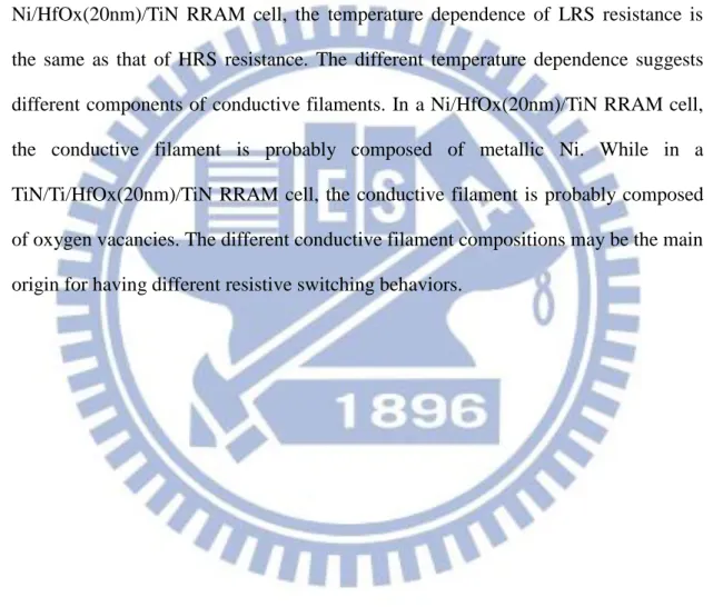
To further understand the current behavior of RRAM cells, it is important to clarify what conduction mechanism is dominant in HRS and LRS. It is well-known that the conduction in RRAM cells is related to trap density significantly, the conduction mechanisms that don’t consider the effect of trap states such as Schottky emission or Fowler-Nordheim (FN) tunneling are ruled out because the RRAM cells always have large trap density after forming process. Direct tunneling is also ruled out because the oxide thicknesses of RRAM cells in this work are larger than 10nm. Some possible conduction mechanisms are listed as follows:
(i) Poole-Frenkel emission: [38]
To detrap the electrons that are captured by trap states, the electrons must receive enough energy to overcome the potential barrier. The electrons could be detrapped by thermionic emission as the Schottky effect. In Poole-Frenkel emission, the barrier heightreduces in the presence of electric field as depicted in Fig. 1-6, so the electrons are easier to accomplish the thermionic emission process with less energy. The current density due to Poole-Frenkel emission can be described as the following,
, (1)
where is the trap energy level with respect to the conduction band, and
is the Poole-Frenkel constant that is related to the extent of field
induced barrier lowering.
(ii) Space charge limited current:
Some reports have shown that the dominant current transport in RRAM cells is space charge limited current (SCLC) [27][39]. When an electric field is applied, the free carrier concentration in an insulator increases as the carriers are injected from the cathode. The space-charge effect occurs when the injected carrier concentration is
9
larger than its thermal equilibrium value, and the following injected carriers will be influenced by the space charges. The current behavior with the space-charge effect is called SCLC.
The trap states influence the SCLC characteristics significantly because the injected carriers are not always free, but could be captured by the trap states as well. Typical I-V characteristics of SCLC when deep traps are present in an insulator is constituted of an Ohmic region and a trap-free square law region , while an additional shallow-trap square law region between them when shallow traps are present, as depicted in Fig. 1-7. The current density in shallow-trap square law region is of the following form [40],
, (2) where
denotes the ratio of free carrier concentration to
the trapped carrier concentration, and L is the thickness of insulator film.
(iii) Trap-assisted tunneling:
The trap-assisted tunneling (TAT) model has been suggested to be the main conduction mechanisms in HfOx based RRAM cells [36]. In TAT model, the traps in
an insulator serve as tunneling sites for carriers. Electrons can transport from anode to cathode by multiple tunneling steps through the traps. Houng et al. [41] have given an approximate formula that relates the current density with the electric field and trap energy level, which is applicable at high electric field region, and is expressed as,
, (3)
where mox is the effective mass of the electron in oxide, and is the trap energy
10
1-5 Objectives
In this work, we fabricate bipolar RRAM cells consisting of TiN/Ti/HfOx/TiN
and unipolar cells consisting of Ni/HfOx/TiN. Since the parameters of RRAM such as Vset, resistances of HRS and LRS depend not only on the materials of the cells but also the operation conditions such as compliance current and stop voltage during reset, we try to find out the relationship between these parameters and operation conditions in this work. Furthermore, we try to give explanations to the switching mechanisms of these cells with our results.
1-6 Thesis Organization
This thesis is divided into four chapters with contents stated as follows in addition
to this chapter.
In Chapter 2, we will describe the fabrication process of TiN/Ti/HfOx/TiN and
Ni/HfOx/TiN RRAM cells. Furthermore, we will present the measurement
configurations and describe the basic electrical characteristics of bipolar switching and unipolar switching, respectively.
In Chapter 3, we will present the characteristics of our RRAM cells and discuss the influence of compliance current and stop voltage during reset on set voltage, resistances of HRS and LRS. And we will discuss the switching mechanisms of these cells with our results. The electrical characteristics with external 1T-1R configuration are also presented in this chapter to discuss the overshoot phenomenon.
Finally, we will summarize our results, and give some advices and suggestions for future study in Chapter 4.
11
Chapter 2
Device Fabrication and Measurement Setup
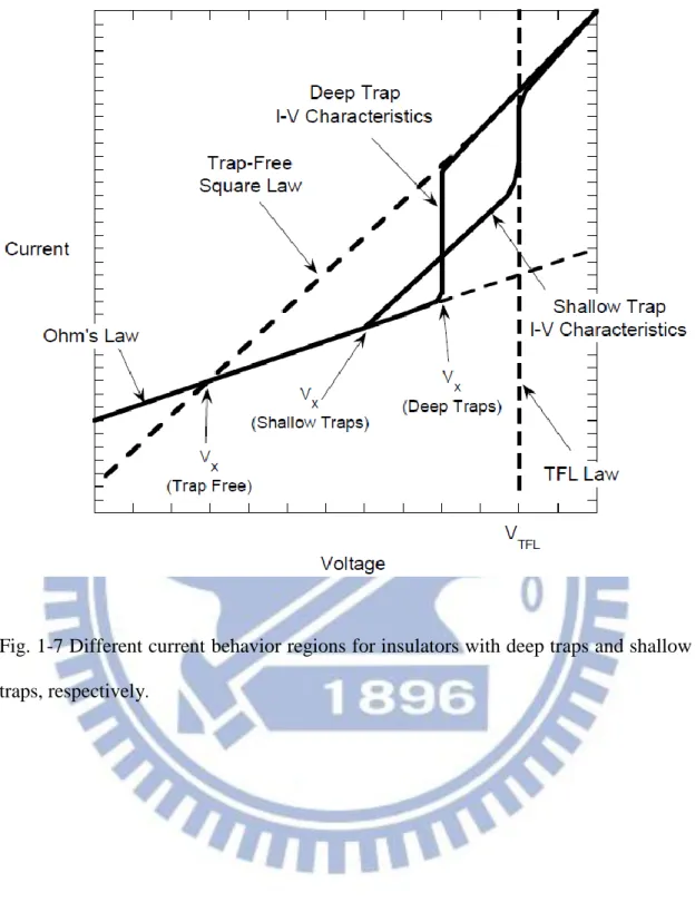
2-1 Device Fabrication and Process Flow
First, a 100 nm-thick TiN was deposited by reactive sputtering as the bottom electrode on a wafer capped with a 100 nm-thick wet oxide. HfOx films with various
thicknesses were then deposited on the TiN, also by reactive sputtering. Finally, Ni or TiN/Ti top electrodes with area of 100 um x100 um was deposited on the HfOx by DC
sputtering and patterned by using a shadow mask. The final device structure is shown in Fig. 2-1.
2-2 Measurement Setup
2-2.1 1R configuration
The I-V characteristics were investigated using an HP4156 system. During the forming/set operations, a compliance current was usually set to limit the cross section of the conductive filaments or, in other words, to limit the magnitude of energy released in the RRAM cells during the soft-breakdown process. Without this setting, excessive leakage current or even hard breakdown would be triggered and affect the regular operation of the memory devices. However, it has been pointed out [43] that the actual current during forming/set operation may exceed the compliance current given by the instrument. The overshoot current could be due to the relatively slow instrument response speed as compared with the fast switching speed of RRAM cells, or the existence of parasitic capacitances [43]. It leads to a higher current during reset operation than expected, and may affect the analysis of the RRAM characteristics. In 1R measurement, to ignore the influence of overshoot current, it is better to set
12
the value of the compliance current higher than 1 mA, from the fact that the relationship of usually holds only when the compliance current is larger than 1 mA, while the Ireset was observed to be around 1 mA with large
variation. When the compliance current is smaller than 1 mA, the overshoot current in the reset process would result in a large variation in the results, as has been reported in many literatures [43].
2-2.2 External 1T1R configuration
So far the configuration with the RRAM cell connected in series with a transistor
has been widely used. The reasons for using such a configuration may be: (1) Add a selection device to eliminate cross-talk issue, i.e., eliminating the sneak path current in a crossbar array that makes it difficult to distinguish between the HRS and LRS. (2) Provide an additional resistance in series with the RRAM cell during reset operation. The voltage drop contributed by the transistor would help the RRAM avoid unwanted set transitions immediately after reset process [44]. (3) Improve the overshoot issue during the set process by eliminating the parasitic capacitance between the RRAM cell and the current limiter [45] (i.e., the transistor in 1T1R configuration).
The output characteristics of the transistor used in this work are shown in Fig. 2-2. The output characteristics have a saturation region, so the current flowing through RRAM cell in series with the transistor is limited by the saturation current of the transistor. Because the saturation current changes with gate voltage, the compliance current of the RRAM cell can be determined by Vg. For example, the compliance current is around when the gate voltage is 4 V in this case. It should be mentioned emphatically that the transistor contained in the 1T1R configuration tested in this work is not integrated with the RRAM cell on the same wafer, as that employed in previous work [46]. On the other hand, the transistor is
13
discrete from the RRAM cell and is connected externally in series during the measurement.
2-3 Unipolar and Bipolar Modes
It is well known that the types of switching operations performed on RRAM
cells can be categorized into bipolar and unipolar modes. The switching type of the RRAM cell is determined by a number of factors, such as the materials of the top/bottom electrodes and the insulator, the compliance current applied during the forming/set process [47], and the polarity of the voltage applied to the cell during the forming process [13].
In the bipolar operation (Fig. 2-3(b)), the voltage polarity during set process is
opposite to that during reset operation. Conversely, in the unipolar operation (Fig. 2-3(a)), the voltage polarity during set process is the same as that of the reset process. In general, both the bipolar and unipolar operations need a forming process in the first switching cycle, and it usually needs a much larger voltage than the set voltage in the following cycles.
The current compliance is an important parameter that has a direct influence on the on/off ratio, the reset current, and the power consumption during the set/reset processes. It has been reported that the magnitude of the compliance current is related to the physical mechanisms of the filament formation/rupture [47], and is thus determinant to the switching type of the cell.
The resistances of the LRS and HRS are determined by the read voltage divided by the currents after set and reset processes, respectively. Like the other types of memories, a larger memory window (that is, the ratio of the resistances of LRS and HRS) of RRAM is always preferable so the sensing circuits are easier to distinguish
14
between the on state and off state. However, the resistances of RRAM, especially the resistances of HRS, usually have a large variation from cycle to cycle. Although there are some special set/reset operation schemes reported to improve the switching uniformity [48], it remains an important issue for practical applications about how to eliminate the variation of the switching parameters of RRAM during operation.
15
Chapter 3
Results and Discussion
3-1 Characteristics of Ni/HfOx/TiN RRAM Cells
3-1.1 Basic 1R switching characteristics of Ni/HfO2/TiN cells
It has been reported that the HfOx based RRAM cell with Ni as the electrode
shows good endurance in unipolar switching [49], and along with its good CMOS compatibility, it is attractive and worth exploring.
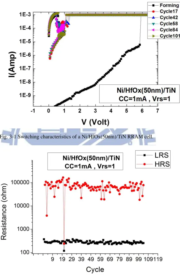
Fig. 3-1 shows the switching characteristics of a fresh Ni/HfOx(50nm)/TiN cell with compliance current of 1 mA. The stop voltage during the reset sweeping is 1 volt. Successive 100 switching cycles are achieved in this device. Both the set and reset operations were done with positive voltage. Abruptly decreased current is observed in the reset switching, consistent with what has been reported [49][50].
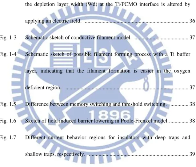
Resistances of high-resistance state/low-resistance state (LRS/HRS) during the successive 100 cycles are shown in Fig. 3-2. The on/off ratio is around 400 in the Ni/HfOx(50nm)/TiN cell with the operation condition mentioned above. As a matter of fact, the on/off ratio is actually tunable with appropriate operation condition, and will be discussed later.
3-1.2 Effects of the compliance current
The compliance current is one of the most important operation parameters that influence the LRS resistance directly. Fig. 3-3 shows the relationship between the LRS resistance and the compliance current obtained from the characterization of the Ni/HfOx(40nm)/TiN cells. Also shown in the figure is the standard deviation of the LRS resistance. It can be clearly seen that the average LRS resistance decreases with increasing compliance current. It is also observed that the cycle-to-cycle variation of
16
LRS resistances can be ignored when the compliance current is sufficiently large. The variation becomes obvious when the compliance current is smaller than 1 mA. It is probably due to the uncontrollable filament size in the presence of overshoot current during the set operation. When the compliance current is small, the overshoot current caused by the charges released from the parasitic capacitance [45] could be larger than the compliance current. The uncontrollable filament size makes it difficult for low power operation.
Another indicator of the filament size is the reset current at which the resistance starts to increase during the reset operation. Fig. 3-4 shows the relationship between the compliance current and the reset current. The reset current decreases with increasing compliance current when it is approximately larger than 0.1 mA, but almost no influence related to the compliance current when it is smaller than 0.1 mA. As the LRS resistance, the cycle-to-cycle variation of reset current is obvious when the compliance current is smaller than 1 mA, but negligible when larger than 1 mA. Fig. 3-5 shows the cumulative probability of HRS resistances of Ni/HfOx(40nm)/TiN RRAM cells with various compliance current. It seems that the compliance current has no significant influence on HRS resistance.
3-1.3 Effects of reset stop voltage
There are few works discussing the influence of the stop voltage during the reset operation Some of the papers described the parameters such as set voltage and HRS resistance of their devices with fixed stop voltage [25][51]. However, it seems not as easy to describe these parameters as they did. Instead, these parameters should be clarified more precisely with the measurement conditions including compliance current and stop voltage during reset (denoted as Vrs in the following discussion). Fig. 3-6(a) shows the cumulative probability of HRS resistances with various Vrs.
17
The HRS resistances also tend to increase with the Vrs, as the case in set voltage. Fig. 3-6(b) shows the cumulative probability of HRS resistances with different HfOx thickness and Vrs of 1 volt. We can find out that the influence of oxide thickness seems not as obvious as the Vrs. The importance of the Vrs can also be observed form Fig. 3-7, in which Fig. 3-7 (a) shows the relation of forming voltage with the oxide thickness, and Fig. 3-7 (b) shows the relation of set voltage with oxide thickness, both with Vrs of 1 volt. It can be obviously seen that the forming voltage increases with increasing HfOx thickness. Because the forming process needs a critical electric field in the HfOx layer to form conductive filaments, the thicker cells need a larger voltage to achieve it. But the thickness of HfOx seems to have no influence on the set voltage when the Vrs remains unchanged,. In contrast, Fig. 3-7(c) shows the relation of set voltage with Vrs with HfOx of 40 nm. It is observed that the set voltage increases with increasing Vrs.
3-2 Characteristics of TiN/Ti/HfOx/TiN RRAM Cells
3-2.1 Basic switching characteristics of TiN/Ti/HfO2/TiN cells
The HfOx-based RRAM cell with Ti electrode has been reported to have excellent bipolar performance, with good endurance and retention. More significantly, low power switching has been achieved in such cells, which is important for high density integration [27].
Fig. 3-8 shows the bipolar switching characteristics of a TiN/Ti/HfOx/TiN cell with compliance current of 0.1 mA. Unlike the Ni/HfOx/TiN cells, the resistance of TiN/ Ti/HfOx/TiN RRAM cell increases gradually during reset operation, which is in agreement with the results reported previously [27].
18
3-2.2 Effects of compliance current
Fig. 3-9 shows the switching behaviors of a TiN/Ti/HfOx(20nm)/TiN RRAM
cell with different compliance currents. The on/off ratio degrades when the compliance current is increased. With the same Vrs, the cell with larger compliance current has lower HRS resistance. It is probably caused by the formation of multiple conductive filaments or filaments with a larger cross section that makes the filaments more difficult to rupture during the reset operation. It seems not to be consistent with the results of Ni/HfOx/TiN RRAM cells, in which the compliance current has no influence on HRS resistances, as has been discussed in previous section.
Although the compliance current indeed affects the resistive switching characteristics, the 1R measurement configuration with overshoot current makes it difficult to show stable switching behavior with a given compliance current. As shown in Fig. 3-10, the TiN/Ti(20nm)/HfOx(20nm)/TiN RRAM cell successfully accomplishes 100 cycles only if we modify the compliance current to an appropriate value when the on/off ratio degrades cycle by cycle.
3-2.3 The dependence of forming voltage on reset current
Fig. 3-11 shows the relationship between the forming voltage and the reset current during the first reset process. We can observe that the reset current increases with increasing forming voltage. It is consistent with the result of a previous study
[52], in which they claimed that the overshoot current during the forming operation depends on the forming voltage. This conception can be easily understood from Fig. 3-12. With a larger forming voltage, more charges are stored in the parasitic capacitance before the cell reaches the forming voltage, resulting in larger overshoot current when the cell reaches the forming voltage.
19
uncontrollable switching behavior. Fig. 3-13(a) shows a TiN/Ti/HfOx/TiN RRAM cell with forming voltage of approximately 4 V, the reset current in the following reset operation is approximate 0.6 mA. In the first set operation, the current reaches the compliance current before the cell reaches the set voltage, resulting in failed set operation. Fig. 3-13(b) shows a TiN/Ti/HfOx/TiN RRAM cell with forming voltage of approximately 1.5 V, and the reset current in the following reset operation is approximate 0.2 mA. Unlike the case mentioned above, the following set operation is successfully completed because of the smaller reset current during the first reset operation. The two cases reveal the importance for lowering the forming voltage in the 1R configuration because of the inevitable overshoot current.
3-2.4 The influence of Ti buffer layer thickness
It has been reported that the Ti buffer layer is able to degrade the dielectric
strength of the dielectric layer [53]. It is because of the interfacial layer formed between the Ti buffer layer and the dielectric layer. The thickness of the Ti buffer layer and the dielectric layer must be optimized for steady switching behavior [53]. TiN/Ti/HfOx/TiN RRAM cells with different thicknesses of Ti buffer layer and HfOx was fabricated and characterized in this work. Major properties including the breakdown field, initial resistance, and the switching ability are summarized in Table 3-1.
Fig. 3-14(a) shows the influence of Ti buffer layer thickness on TiN/Ti/HfOx(10nm)/TiN RRAM cell. With 20 nm Ti buffer layer, the fresh cell is too leaky to form local conductive filament, and thus no switching behavior can be observed. With 10 nm Ti buffer layer, the leakage current of the fresh cell is reduced and the cell shows switching behavior, but failed in switching within 5 cycles. Without Ti buffer layer, the leakage current of the fresh cell is further reduced but
20
failed in reset operation. Fig. 3-14(b) shows the characteristics of TiN/Ti/HfOx(20nm)/TiN RRAM cells with various thickness of Ti buffer layer. The fresh cell with 20 nm Ti buffer layer also shows largest leakage current and the lowest forming voltage, and it can switch more than 5 cycles. The cell with 10 nm Ti buffer layer shows lower leakage current and higher forming voltage, and its switching ability is less than 5 cycles. Without Ti buffer layer, the cell fails in forming operation because it has the best dielectric strength. Among them, the RRAM cell with 20 nm Ti buffer layer and 20 nm HfOx dielectric layer shows the most stable switching behavior.
3-3 Switching Characteristics of Ni/HfOx/TiN Cells
with External 1T1R Configuration
In order to eliminate the overshoot current, we have tried to use external 1T1R configuration in this work. In forming/set process, Vg of 4 volt is applied to the transistor, and the compliance current for RRAM cell is approximately 0.2 mA (see Chap. 2). In reset process, the voltage is applied to the RRAM cell directly without involving the transistor. Note that in the 1T1R configuration reported in the literature, the two devices were integrated together and the RRAM cell was connected to the drain of the transistor, Vg larger than that in forming/set process must be applied to the transistor in reset process. In our configuration, the RRAM cell and the transistor were fabricated independently, thus we can choose not to connect the transistor with the RRAM cell during reset operation so as to simplify the analysis.
Fig. 3-15 shows the switching characteristics of a Ni/HfOx(40nm)/TiN RRAM cell in our external 1T1R configuration. It can be observed that the reset current is still much larger than the compliance current as in 1R configuration. This indicates that
21
the overshoot current still exists in the external 1T1R configuration. However, we can point out that the overshoot current is mainly caused by the existence of parasitic capacitance, rather than the slow response speed of the measurement instrument, as has been reported elsewhere [45].
3-4 Comparison between RRAM Cells with Ni and TiN/Ti
Top Electrodes
3-4.1 Switching mechanism
Despite many efforts put into studies in these years, the mechanism of resistive switching is still in debate. The analyses of switching mechanism were mostly based on qualitative descriptions. In addition, there is a lack of quantitative analyses describing the switching procedure of a RRAM cell for it to achieve real application in IC industry.
Most of reports described the resistive switching mechanism of Ti/HfOx based RRAM cell using VCM model that has been mentioned in Chapter 1. The resistive switching is attributed to the formation/rupture of conductive filaments that are composed of oxygen vacancies in HfOx [28][54]. However, some reports related the resistive switching behavior to the charge trapping/detrapping process, which influenced the magnitude of space-charge-limited current [27].
There were also several models that have been reported to describe the switching behavior of the Ni/HfOx-based RRAM cell. For example, the switching behavior is suspected to be related to the filament composed of Ni ions [13][49]. Under the forming operation, the Ni ions migrate from the top electrode in the presence of electric field and form conductive paths that connect the top and bottom electrodes, so that the cell is switched to LRS. The size of the filaments is controlled by the
22
compliance current with the measurement instrument. Under the reset operation, the filaments are annihilated by the Joule-heating that is induced by the current flow as a voltage is applied. Another contention says that the Ni/HfOx-based cells switch with the presence of a NiOx layer at the interface between Ni and HfOx [12]. As the forming action is done, both the NiOx and the HfOx suffer from soft-breakdown procedure and form conductive filaments composited of oxygen vacancies. As for reset operation, the filaments in the NiOx film are annihilated because of the Joule-heating induced re-oxidation reaction, while the filaments in the HfOx film remain.
More efforts such as material analysis or electrical measurement must be further taken to certify the switching mechanisms. In this work, we have studied the electrical characteristics of our devices under various operation conditions. In the following sections, we try to distinguish the conduction behaviors of TiN/Ti/HfOx/TiN RRAM cells and Ni/HfOx/TiN RRAM cells with IV curve fitting and measurements with varied temperature.
3-4.2 Conduction mechanism
In order to verify the property of the conductive filaments, it is worthy to study the conduction mechanism of the RRAM cell. Figs. 3-16(a) and (b) show the I-V characteristics of fresh Ni/HfOx(20nm)/TiN and TiN/Ti/HfOx(20nm)/TiN RRAM cells, respectively. Both show asymmetric I-V behaviors, implying that the current of fresh RRAM cells are contact-controlled Schottky conduction that is dependent on the work functions of the electrodes. However, the current behaviors of RRAM cells are no longer contact-controlled after forming operation. As shown in Fig. 3-17, in which both HRS and LRS show highly symmetric current behaviors. It is probably caused by the high trap density of the HfOx after forming process.
23
The I-V characteristics of a Ni/HfOx(20nm)/TiN RRAM cell in LRS is shown in Fig. 3-18(a). We can observe that the I-V curve shows linear behavior before the cell reaches reset voltage, and we can say that the conduction mechanism of Ni/HfOx(20nm)/TiN is ohmic in nature. On the other hand, the HRS current of a Ni/HfOx(20nm)/TiN RRAM cell can be well fitted using Poole-Frenkel conduction model, as shown in Fig. 3-18(b). Fig. 3-19(a) shows the I-V characteristics of a TiN/Ti/HfOx(20nm)/TiN RRAM cell in LRS. The I-V curve consists of an ohmic conduction region and a square-law region before the cell reaches reset voltage, which is consistent with that reported elsewhere [27]. Such I-V behavior suggests that the possible conduction mechanism is space-charge-limited current (SCLC) [40]. As shown in Fig. 3-19(b), the HRS I-V curve consists of an ohmic conduction region and a square-law region, and an additional region with the slope increases rapidly, Qi Liu
et al. suggests that this region corresponds to a trap filling process [39]. From this point of view, the resistive switching is probably attributed to the trapping and de-trapping processes. In HRS, the trap sites are empty, and the current behavior follows trap-controlled SCLC. And in LRS, the trap sites are filled, the current behavior follows trap-free SCLC.
3-4.3 Temperature dependence
Fig. 3-20(a) shows the temperature dependence of both HRS resistance and LRS resistance of a Ni/HfOx(20nm)/TiN RRAM cell. We can observe that the resistance decreases with increasing temperature in HRS while increases with increasing temperature in LRS. The temperature dependence of resistance in HRS is attributed to the hopping conduction between the trap sites, and the hopping probability increases with increasing temperature, leading to the lowering in resistance [13]. In LRS, the temperature dependence of resistance suggests that the Ni/HfOx(20nm)/TiN RRAM
24
cell exists metallic conduction paths. As temperature increases, the probability of both impurity scattering and phonon scattering increases, leading to increasing resistance. The temperature dependent LRS resistance of Ni/HfOx/TiN RRAM cell can be expressed as [55],
, (1) where R0 is the resistance at the reference temperature T0, and α is the temperature
coefficient of resistance. From the slope of resistance-temperature curve, we can extractα =4.6*103 K-1.
Fig. 3-21 shows the I-V curve of a Ni/HfOx(20nm)/TiN RRAM cell in LRS, also shown in Fig. 3-21 is the temperature calculated using the extracted α value and the continuously changing resistance before the cell reaches reset voltage. The temperature can be considered as the local temperature of the conductive filament, and the temperature at reset voltage can be considered as the critical temperature for reset switching. The evaluated value of critical temperature is 395K, and it is very close to the resistance-temperature curve shown in Fig. 3-22, in which the resistance increases obviously at around 380K. This result gives an evidence for us to say that the reset switching in a unipolar RRAM cell is accomplished by joule heating.
As has been mentioned in previous section, the HRS current behavior of Ni/HfOx(20nm)/TiN RRAM cell can be well fitted using the Poole-Frenkel model. Fig. 3-23 shows ln(I/V) versus 1/kT under different biases, which follows Arrhenius relation. The activation energy (Ea) can be extracted from the slope. As we plot the activation energy against the applied biases as shown in Fig. 3-24, we can extract the trap energy level from the intersection on y-axis. Based on Poole-Frenkel model, the slope in Fig. 3-24 is equal to
, in which L is the thickness of HfOx, and the
25
is about 0.29 eV, which is very close to that reported previously [56]. The extracted dielectric constant of HfOx is around 34.7, not far from the reported values (25-30)
[57], showing some credibility for us to describe the HRS conduction behavior of Ni/HfOx/TiN RRAM cells in term of Poole-Frenkel model.
Fig. 3-20(b) shows the temperature dependence of both HRS resistance and LRS resistance of a TiN/Ti/HfOx(20nm)/TiN RRAM cell. Unlike the situation in a Ni/HfOx(20nm)/TiN RRAM cell, the temperature dependence of LRS resistance is the same as that of HRS resistance. The different temperature dependence suggests different components of conductive filaments. In a Ni/HfOx(20nm)/TiN RRAM cell, the conductive filament is probably composed of metallic Ni. While in a TiN/Ti/HfOx(20nm)/TiN RRAM cell, the conductive filament is probably composed of oxygen vacancies. The different conductive filament compositions may be the main origin for having different resistive switching behaviors.
26
Chapter 4
Conclusion and Future Work
4-1 Conclusion
In this thesis, Ni/HfOx/TiN and TiN/Ti/HfOx/TiN RRAM cells with various
thicknesses of HfOx have been fabricated. The electrical characteristics with various operation parameters such as compliance current and stop voltage during reset operation (Vrs) were investigated. We also explored the influences of the HfOx thickness and operation parameters on HRS/LRS resistances, set voltages and reset current, as well as the influences of Ti buffer layer thickness on the switching behavior. The external 1T1R configuration was used to investigate the origin of overshoot current during forming and set operations. Finally, we compared the properties of conductive filaments, and probed the conduction mechanisms of Ni/HfOx/TiN and TiN/Ti/HfOx/TiN RRAM cells by I-V curves fitting and measurements with varied temperature. Several summaries and conclusions were listed as follows.
(1) The on/off ratio and the operation voltages of a RRAM can be tuned with varied operation parameters. For example, the HRS resistances and set voltages of Ni/HfOx/TiN RRAM cells were dependent on Vrs obviously. Besides, the compliance current during forming and set operations affects the LRS resistance directly. The thickness of HfOx seems to have little influence on the switching characteristics, but it does influence the forming voltage significantly.
27
compliance current. However, the overshoot current is significant and not negligible when the compliance current is less than 1mA. Hence, the forming voltage of TiN/Ti/HfOx/TiN RRAM cell must be minimized for reducing the overshoot current. The optimized thickness of HfOx and Ti buffer layers have also been investigated. In this work, we find out that the cell with HfOx of 20nm and Ti buffer layer of 20nm shows the best characteristics, which can switch over 100 cycles under the condition of compliance current less than 0.5mA and Vrs of -2.5V.
(3) The external 1T1R configuration does not eliminate the overshoot issue which hinders the low current operation in 1R configuration. However, the results still provide insight for us to believe that the overshoot current is mainly caused by the existence of parasitic capacitance in the instrument, rather than the slow response speed of the measurement instrument. As has been reported [45], the overshoot current can be eliminated by the 1T1R configuration in which the RRAM cell is integrated on the drain side of the transistor.
(4) The temperature dependences of Ni/HfOx/TiN and TiN/Ti/HfOx/TiN RRAM cells on resistances are different. The I-V curve of those devices could be fitted using different conduction models, from which different properties of conductive filaments can be understood. We believe that the conductive filaments in Ni/HfOx/TiN RRAM cells are composed of Ni ions, but oxygen vacancies in TiN/Ti/HfOx/TiN RRAM cells.
In this work, we find out that the RRAM cells show flexible switching parameters, which is an important concept for industrial use. The effects of the Ti buffer layer with different thickness are investigated, giving us a process factor that can be considered in RRAM cells design. Besides, the external 1T1R configuration fails in eliminating the overshoot current issue. For practical applications the RRAM cells should be integrated with the transistors to suppress the influences of parasitic
28
capacitance. Finally, different current conduction behaviors of RRAM cells with different electrodes are observed, shedding some light on exploring the mechanisms of resistive switching phenomena.
4-2 Suggestions for Future Work
In this work, it has been demonstrated that the overshoot current during the forming/set operation influences the electrical characteristics significantly, and the external 1T1R fails in eliminating the issue. To make the effects of overshoot current negligible, compliance current larger than 0.1mA is used in this work. However, one of the attractive features of RRAM for the next generation memory is its ability to switch with low operation power. Thus it’s important to investigate the electrical characteristics with lower compliance current. To accomplish this goal, the integrated 1T1R configuration in which the RRAM cell connected to the drain side of the transistor must be used. It should be mentioned that the transistor in the 1T1R configuration is best to have drive current and on/off ratio as large as possible, because that the RRAM cell and the transistor are connected in series during device fabrication. During reset operation, the gate voltage should be larger than that during forming/set operation for the RRAM cell to reach the reset current. With larger drive current and on/off ratio, it is more flexible for choosing appropriate compliance current.
The RRAM cells fabricated in this work show significant cell-to-cell variation, together with the effect of overshoot current, it is in fact very difficult to observe some clear tendencies between the process conditions and electrical characteristics. As has been reported previously [58], downscaling the cell area may improve the
29
variation issue due to the reduction of defects in the cell. Smaller cell area offers additional advantages such as a higher HRS resistance and more efficient local heating effect because of a reduced number of conductive filaments. The compliance current can also be lowered with a smaller cell area because of a lower leakage current of the fresh RRAM cell. Summing up the advantages mentioned above, it is suggested to fabricate RRAM cells with an area much less than that of the devices characterized in this study in the future.
30
References:
[1] B. J. Choi, D. S. Jeong, S. K. Kim, C. Rohde, S. Choi, J. H. Oh, H. J. Kim, C. S. Hwang, K. Szot, R. Waser, B. Reichenberg, and S. Tiedke, ―Resistive switching mechanism of TiO2 thin films grown by atomic-layer deposition,‖ J. Appl. Phys., vol. 98, no.3, pp.033715-1 -033715-10, Jan. 2005.
[2] S. Q. Liu, N. J. Wu, and A. Ignatiev, ―Electric-pulse-induced reversible resistance change effect in magnetoresistive films,‖ Appl. Phys. Lett., vol. 76, no.19, pp. 2749-2751, Mar. 2000.
[3] C. Kügeler, M. Meier, R. Rosezin, S. Gilles, and R. Waser,, ―High density 3D memory architecture based on the resistive switching effect,‖ Solid-State Electron., vol. 53, no.12, pp. 1287-1292, Dec. 2009.
[4] T. W. Hickmott, ―Low‐frequency negative resistance in thin anodic oxide films,‖ J.
Appl. Phys., vol. 33, no.9, pp. 2669-2682, Feb. 1962.
[5] J.F. Gibbons, and W.E. Beadle, ―Switching properties of thin NiO films,‖
Solid-State Electron., vol. 7, no.11, pp. 785-790, Nov. 1964.
[6] J.G. Simmons and R.R. Verderber, ―New thin-film resistive memory,‖ Radio
Electron. Eng., vol. 34, no.2, pp. 81-89, Aug. 1967.
[7] Y. Hirose and H. Hirose, ―Polarity‐dependent memory switching and behavior of Ag dendrite in Ag‐photodoped amorphous As2S3 films,‖ J. Appl. Phys., vol. 47, no.6,
pp. 2767-2772, Jun. 1976.
[8] A. Sawa, T. Fujii, M. Kawasaki, and Y. Tokura, ―Hysteretic current–voltage characteristics and resistance switching at a rectifying Ti∕Pr0.7Ca0.3MnO3 interface,‖
Appl. Phys. Lett., vol. 85, no.18, pp. 4073-4075, Sep. 2004.
[9] K. Kinoshita, T. Tamura, M. Aoki, Y. Sugiyama, and H. Tanaka, ―Bias polarity dependent data retention of resistive random access memory consisting of binary transition metal oxide,‖ Appl. Phys. Lett., vol. 89, no.10, pp. 103509 - 103509-3, Jul. 2006.
[10] R. Waser, R. Dittmann, G. Staikov, and K. Szot, ―Redox-based resistive switching memories – nanoionic mechanisms, prospects, and challenges,‖ Adv. Mater., vol. 21, no.25-26, pp. 2632–2663, Jul. 2009.
[11] A. Sawa, ―Resistive switching in transition metal oxides,‖ Mater. Today, vol. 11, no.6, pp. 28-36, Jun. 2008.
[12] X. A. Tran, W. Zhu, W. J. Liu, Y. C. Yeo, B. Y. Nguyen, and H. Y. Yu, ―Self-selection unipolar HfOx-based RRAM,‖ IEEE Trans. Electr. Dev., vol. 60, no.1, pp. 391–395, Jan. 2013.
[13] K. L. Lin, T. H. Hou, J. Shieh, J. H. Lin, and C. T. Chou, ―Electrode dependence of filament formation in HfO2 resistive-switching memory,‖ J. Appl. Phys., vol.109,
![Fig. 1-1 Sketch of a crossbar array [42].](https://thumb-ap.123doks.com/thumbv2/9libinfo/8121535.165917/51.892.137.763.112.957/fig-sketch-crossbar-array.webp)
![Fig. 1-5 Difference between memory switching and threshold switching [32] .](https://thumb-ap.123doks.com/thumbv2/9libinfo/8121535.165917/53.892.134.766.130.937/fig-difference-memory-switching-threshold-switching.webp)
![Fig. 2-3 Unipolar and bipolar switching schemes. CC denotes the compliance current which is often needed to limit the ON current [15]](https://thumb-ap.123doks.com/thumbv2/9libinfo/8121535.165917/56.892.134.748.111.896/unipolar-bipolar-switching-schemes-denotes-compliance-current-current.webp)