超臨界流體技術應用於非晶矽薄膜電晶體之研究
68
0
0
全文
(2) 超臨界流體技術應用於非晶矽薄膜電晶體之研究 Application of Supercritical Fluids Technology for Amorphous Thin Film Transistors 研 究 生: 王 建 文 指導教授: 劉 柏 村. Student: Chen-Wen Wang 博士. Advisor: Dr. Po-Tsun Liu. 國 立 交 通 大 學 顯 示 科 技 研 究 所 碩 士 論 文 A Thesis Submitted to Department of Photonics & Display Institute College of Electrical and Computer Engineering National Chiao Tung University in Partial Fulfillment of the Requirements for the Degree of Master in Photonics June 2006 Hsinchu, Taiwan, Republic of China. 中 華 民 國. 九十五. 年. 六. 月.
(3) 超臨界流體技術應用於非晶矽薄膜電晶體之研 究. 研究生:王 建 文. 指導教授:劉 柏 村. 博士. 國 立 交 通 大 學 光電工程學系 顯示科技研究所. 摘要. 在此論文裡,我們研究了非晶矽薄膜電晶體在超臨界二氧化碳流體混合水的 熱處理下其電性的改變。非晶矽薄膜電晶體已經被廣泛的使用在液晶平面顯示器 的製造上。電漿輔助化學氣相沉積用來達到在低溫下製造非晶矽薄膜電晶體,但 不可避免地,非晶矽薄膜在沉積過程中因為懸鍵和晶格的錯位,會產生電性上的 缺陷,這些缺陷會捕捉載子而使電流降低。而如何減少這些缺陷密度在非晶矽薄 膜電晶體的製造中是很重要的。 我們發現在超臨界流體的處理下,非晶矽薄膜電晶體有較好的元件特性,其 漏電流、臨界電壓和次臨界擺幅以及場效移動率都有顯著的提升。這些改善是因 為氧原子護佈住了懸鍵。 為了驗證超臨界流體混合水能有效的使矽與氧鍵結,我們使用了紅外線光譜 儀量測薄膜的吸收光譜。除此之外還使用了接觸角量測以及熱脫附常壓游離質譜 儀來分析與比較。 這些結果均顯示,藉由超臨界流體中的氧護佈,能減少薄膜的缺陷密度。可 i.
(4) 預期的,超臨界流體的特殊特性將使其整合在 TFT-LCD 製程上具有其優勢。. ii.
(5) Application of Supercritical Fluids Technology for Amorphous Thin Film Transistors. Student:Chen–Wen Wang. Advisor:Dr. Po-Tsun Liu. Department of Photonics and Display Institute National Chiao Tung University. Abstract. In this thesis, the changes in electrical properties induced by heat treatment with supercritical CO2 fluid interfuse H2O are researched for amorphous TFTs. Amorphous silicon thin film transistors (a-Si TFTs) have been widely applied to fabrication of liquid crystal flat-panel display. Plasma enhancement chemical vapor deposition (PECVD) have been used for fabrication of a-Si TFTs at low temperatures. Inevitable amorphous silicon films among deposition have electrically active defect states because of dangling bonds and lattice disorder. The defects reduce electrical current due to trapping carriers. One of most important problems on fabrication of a-Si TFTs is the reduction of densities of those defect states. It is found that the a-Si TFTs after supercritical fluid passivation could achieve better device performances, including the off-current and the threshold voltage and the subthreshold swing, and also better filed effect mobility. These improvements were attributed to the oxygen atoms passivation of the dangling bonds. In order to demonstrate the incorporation of oxygen in silicon films by the supercritical fluid passivation interfuse H2O, infrared absorption spectra were measured using fourier transform infrared spectroscopy (FTIR). In addition, contact angle and thermal desorption spectroscopy (TDS) were also been used. These results show that the supercritical fluid passivation interfuse H2O reduces iii.
(6) the defect density in the silicon films with oxygen incorporation. With the excellent characteristic, supercritical fluids will have advantages of integrating into the fabrication of TFT-LCD’s.. iv.
(7) 誌 謝. 經過兩年的努力,終於順利獲得了碩士的學位。在這段研究生涯中,有太多 人令我心存感激。首先,要特別感謝我的論文指導老師 劉柏村教授,感謝老師 的指導、教誨和鼓勵,不僅僅是在學術研究上的指導,對於人生規劃及待人處事 的態度上,亦讓我獲益良多,使我能順利的完成碩士學位。另外,還要感謝中山 物研所 張鼎張教授,在學術研究上給我正確詳盡的指導,在此致上內心最誠摯 的敬意和謝意。諸位口試委員的指導和建議,也在此謹申謝意。 此外,特別要感謝蔡志宗學長在實驗、量測分析以及論文寫作給予我莫大的 協助與建議,使我順利獲得知識與學位。還有要感謝吳興華學長、李泓緯學長、 黃震鑠學長、盧皓彥學長、陳世青學長、吳永俊學長、周政偉學長以及謝永龍學 長,感謝學長們平日對我的照顧以及研究上的建議。也要感謝實驗室一起工作的 同學-李逸哲、陳弘根、鄒一德、蘇可青、陳建焜、邱皓麟、高鈺函…等,以及 學弟妹-楊柏宇、李昇翰、黃千睿、曾子怡、聶建名、陳又菁、鍾宛芳、蕭秀娟、 李啟銘、李崇維、葉唐豪、趙育德、施偉倫…等,感謝你們陪伴我共同走過這一 段甘甜的日子,讓我無論是在實驗中或是讀書時永遠充滿歡樂。同時,衷心感謝 國家奈米元件實驗室(NDL)和交大半導體中心提供良好的研究設備與充足的資 源。 最後,我願將這份榮耀呈獻給我深愛的父母親- 王清富先生、 楊秀菊女 士。感謝父母親多年來辛苦的教導與栽培,一直在背後默默地支持與關懷我,陪 我度過了許多風雨與榮耀的時光,讓我能無後顧之憂,全力衝刺學業,終於不負 所望完成學業,在此獻上我內心最深的謝意。此外,特別要感謝陪伴我多年的摯 友-黃雅絹,一直以來因為妳的支持及協助,使我能順利的從大學畢業到現在碩 士論文的完成,在此由衷的對妳說聲謝謝。 王建文 2006 年 6 月. v.
(8) Contents Chinese Abstract. ----------------------------------------------------------------i. English Abstract. -------------------------------------------------------------- iii. Chinese Acknowledgment Contents. ----------------------------------------------------v. -------------------------------------------------------------------------vi. Table Captions. ----------------------------------------------------------------vii. Figure Captions. --------------------------------------------------------------viii. Chapter 1. Introduction 1.1 General Background. --------------------------------------------------- 1. 1.2 Introduction to Supercritical Fluid Processes. -----------------------2. 1.3 Motivation ----------------------------------------------------------------3 1.4 Thesis outline. Chapter 2. ------------------------------------------------------------ 4. Fabrication and Experiment 2.1 Devices Structure and Fabrication. ----------------------------------- 7. 2.2 Experimental Procedures -----------------------------------------------8 2.3 Measurement and Parameter Extraction ----------------------------- 9. Chapter 3. Result and Discussion 3.1 Electrical Analysis. -----------------------------------------------------19. 3.2 Material Analysis ------------------------------------------------------ 24 3.3 Mechanism ------------------------------------------------------------- 26 3.4 Summary ----------------------------------------------------------------32. Chapter 4. Conclusion -------------------------------------------------- 52. References. ------------------------------------------------------------------53. Vita -------------------------------------------------------------------------- 56. vi.
(9) Table Captions. Chapter 1 Table 1-1 Critical temperature and pressure for some common fluids. Table 1-2 Comparison of physical properties of CO2.. Chapter3 Table 3-1 Parameters of a-Si TFTs before and after annealing for 2 hours at 150℃(was measured at Vd=0.1V and T=30℃). Table 3-2 Parameters of a-Si TFTs before and after H2O passivation for 2 hours at 150℃(was measured at linear region and T=30℃). Table 3-3 Parameters of a-Si TFTs before and after SCCO2 passivation for 2 hours at 150℃(was measured at Vd=0.1V and T=30℃). Table 3-4 Contact angle after passivation.. vii.
(10) Figure Captions Chapter 1 Fig. 1-1. Phase diagram for CO2.. Fig. 1-2. Density – pressure – temperature surface for pure CO2.. Chaprer 2 Fig. 2-1. Cross-sectional view of the a-Si TFT.(Conventional back channel etching structure was used). Fig. 2-2. Cross-sectional view of polycrystalline silicon thin film.. Fig. 2-3. Schematic drawing of the supercritical fluids treatment system.. Fig. 2-4. Definition of subthreshold swing (S.S.).. Chapter 3 Fig. 3-1 Transfer characteristics of a-Si TFTs before and after annealing for 2 hours at 150℃(was measured at Vd=0.1V and T=30℃). Fig. 3-2 Transfer characteristics of a-Si TFTs before and after annealing for 2 hours at 150℃(was measured at Vd=0.1V and T=30℃). Fig. 3-3 Transfer characteristics of a-Si TFTs before and after annealing for 2 hours at 150℃ (was measured at Vd=10V and T=30℃). Fig. 3-4. Output characteristics of a-Si TFTs before and after annealing for 2 hours at 150℃ (was measured at T=30℃).. Fig. 3-5. Transfer characteristics of a-Si TFTs before annealing for 2 hours at 150℃(was measured at Vd=0.1V and T=30℃~60℃).. Fig. 3-6. Transfer characteristics of a-Si TFTs after annealing for 2 hours at viii.
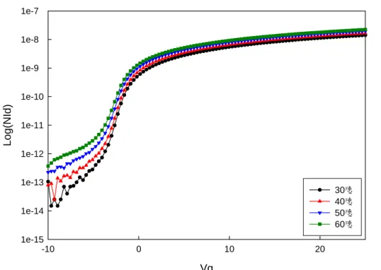
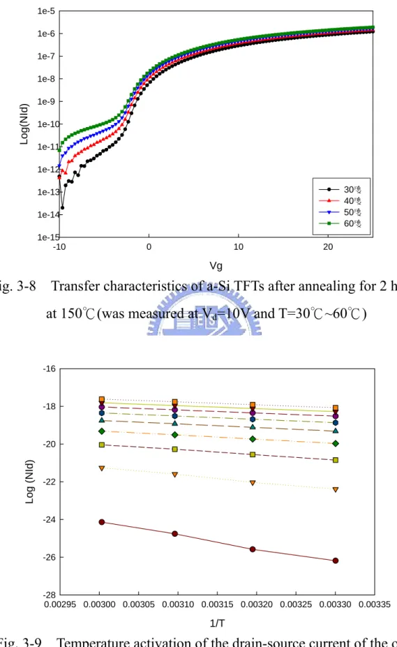
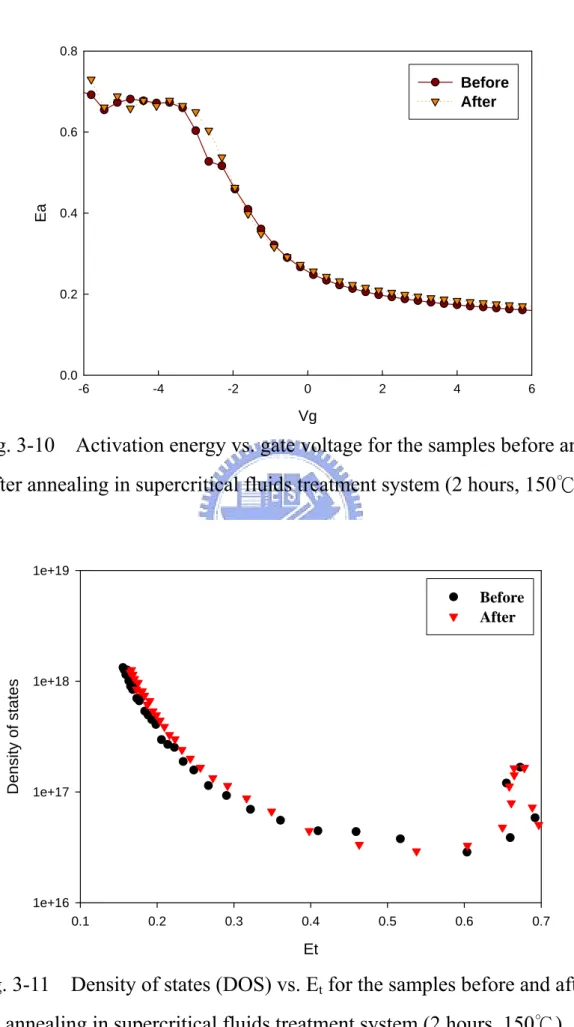
(11) 150℃(was measured at Vd=0.1V and T=30℃~60℃). Fig. 3-7. Transfer characteristics of a-Si TFTs before annealing for 2 hours at 150℃(was measured at Vd=10V and T=30℃~60℃).. Fig. 3-8. Transfer characteristics of a-Si TFTs after annealing for 2 hours at 150℃(was measured at Vd=10V and T=30℃~60℃).. Fig. 3-9. Temperature activation of the drain-source current of the only annealing 2 hours at 150℃ sample (Fig. 3-6) for different gate voltages.. Fig. 3-10. Activation energy vs. gate voltage for the samples before and after annealing in supercritical fluids treatment system (2 hours, 150℃).. Fig. 3-11 Density of states (DOS) vs. Et for the samples before and after annealing in supercritical fluids treatment system (2 hours, 150℃). Fig. 3-12. Transfer characteristics of a-Si TFTs before and after H2O passivation for 2 hours at 150℃(was measured at linear region, T=30℃).. Fig. 3-13. Transfer characteristics of a-Si TFTs before and after H2O passivation for 2 hours at 150℃(was measured at linear region, T=30℃).. Fig. 3-14. Transfer characteristics of a-Si TFTs before and after H2O passivation for 2 hours at 150℃ (was measured at sat. region, T=30℃).. Fig. 3-15. Output characteristics of a-Si TFTs before and after H2O passivation for 2 hours at 150℃ (was measured at T=30℃).. Fig. 3-16 Transfer characteristics of a-Si TFTs before and after SCCO2 passivation for 2 hours at 150℃. (was measured at Vd=0.1V and T=30℃). Fig. 3-17 Transfer characteristics of a-Si TFTs before and after SCCO2 passivation for 2 hours at 150℃. (was measured at Vd=0.1V and T=30℃). Fig. 3-18 Transfer characteristics of a-Si TFTs before and after SCCO2 passivation for 2 hours at 150℃. (was measured at Vd=10V and T=30℃). Fig. 3-19 Output characteristics of a-Si TFTs before and after SCCO2 passivation ix.
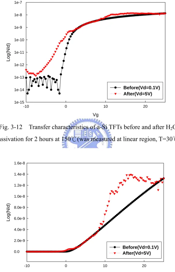
(12) for 2 hours at 150℃ (was measured at T=30℃). Fig. 3-20. Transfer characteristics of a-Si TFTs before SCCO2 passivation for 2 hours at 150℃(measured at Vd=0.1V, T=30℃~60℃).. Fig. 3-21 Transfer characteristics of a-Si TFTs after SCCO2 passivation for 2 hours at 150℃(measured at Vd=0.1V, T=30℃~60℃). Fig. 3-22. Transfer characteristics of a-Si TFTs before SCCO2 passivation for 2 hours at 150℃(measured at Vd=10V, T=30℃~60℃).. Fig. 3-23 Transfer characteristics of a-Si TFTs after SCCO2 passivation for 2 hours at 150℃(measured at Vd=10V, T=30℃~60℃). Fig. 3-24. Activation energy vs. gate voltage for the samples before and after SCCO2 fluid interfuse H2O passivation (2 hours, 150℃).. Fig. 3-25 Density of states (DOS) vs. Et for the samples before and after SCCO2 fluid interfuse H2O passivation (2 hours, 150℃). Fig. 3-26. Infrared absorption spectra after passivation 2 hours.. Fig. 3-27. Infrared absorption spectra after passivation 2 hours and then hot plate baking 1 hour.. Fig. 3-28 Thermal desorption spectroscopy after passivation 2 hours. Fig. 3-29. Thermal desorption spectroscopy after passivation 2 hours and then hot plate baking 1 hour at 200℃.. Fig. 3-30 Contact angle measurement. Fig. 3-31 Density of states (DOS) in the amorphous silicon. Fig. 3-32 Schematic illustration of the basic operation of the a-Si TFT. Fig. 3-33 Drain-source current vs. gate-source voltage of the a-Si TFT. Fig. 3-34 Band diagram for a cross section in the channel area of the a-Si TFT.. x.
(13) Chapter 1 Introduction 1.1. General Background. Since the first amorphous silicon thin film transistor (a-Si TFTs) was reported by LeComber et al. in 1979 [1], many studies have been reported on a-Si TFTs. One of the significant features of the a-Si TFT is its large on-off ratio defined as the ratio of on state current to off state current in the terminal of the drain. Due to this advantageous characteristic, a-Si TFTs have been thought to be suitable for switching elements of an active matrix circuit of a liquid crystal display (AMLCD). As the switching element in active matrix liquid crystal display, the semiconductors such as single-crystal Si [2], polycrystalline Si [3], CdSe [4], and Te [5] have been studied. Among these devices, amorphous silicon is one of the most favorable semiconductors satisfying the requirements for thin film transistors in liquid crystal display. In recent years, amorphous silicon thin film transistors have been widely used in pixel-driving elements of a liquid crystal display. The a-Si TFT is particularly beneficial to the production of large screen displays and mass production. Large scale matrix circuits require switching elements with a large on-off ratio. Greater than six orders of magnitude in a-Si TFTs have been observed. Additionally, the inverted-staggered back-channel-etched type (BCE) hydrogenated amorphous silicon thin film transistor has been popularly employed as the switch to control the gray level in active matrix liquid crystal display (AMLCD) [6-9] and to drive organic light emitting diode (OLED) [10-12]. Therefore, it is important to have stable character of device and better uniformity and lower cost for a-Si TFT. In AMLCD, a-TFT is a switching device to turn on the current path for charging the liquid crystal capacitor and turn off the current path for discharging. Consequently, the leakage current of a-TFT should be low enough to keep on exact gray level before 1.
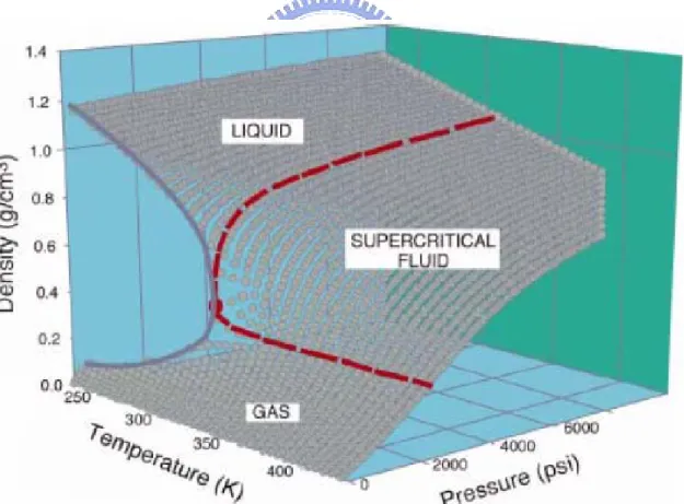
(14) refreshing. On the contrary, the displays reveal incorrect color or rather lack of deep black. However, to reduce fabrication cost, improvement of production yield is vital. Otherwise, some defect reduction methods have been proposed, whether in amorphous Si-TFTs or polycrystalline Si-TFTs.. 1.2. Introduction to Supercritical Fluid Processes Supercritical fluids are compounds above their critical temperatures and pressure.. Fig 1-1 [13-14] and Table 1-1 present critical temperature and pressure for some common fluids, which are used in many commercial applications, including the extraction of caffeine from coffee, fats from foods, and essential oils from plants for use in perfumes. CO2-based supercritical fluids are particularly attractive because CO2 is non-toxic, non-flammable, and inexpensive. Its critical conditions are more achievable with existing process equipment (31 ℃ , 1072 psi =72.8 atm). The attractiveness of supercritical fluids for commercial applications is their unique combination of liquid-like and gas-like properties. Table 1-2 shows the comparison of several physical properties of typical liquid, vapor, and supercritical fluid state. It can be seen that high density of supercritical fluids possesses a liquid-like density. This gives the fluid the ability, much like that of a light hydrocarbon (i.e. pentane), to dissolve most solutes [15]. Also supercritical fluids are gas-like in respect to their very low viscosity and little to no surface tension allowing them to enter the smallest pores or spaces on a wafer. These properties make supercritical fluids so appealing for cleaning, extraction, and chromatography [16]. Figure 1-2 shows the density-pressure-temperature surface for pure CO2. It can be seen that relatively small changes in temperature or pressure near the critical point could result in large changes in density. These properties make supercritical fluid technology so attractive for many applications. To put it briefly, supercritical CO2 fluid is one of the green solvents. It possesses 2.
(15) the high density property like liquid, so it can transport more Supercritical fluid than liquid. And supercritical CO2 has diffusivity greater than liquid, allowing for rapid transport properties. Besides, the absence of surface tension provides for excellent mass transport into micro-porous matrices.. 1.3. Motivation. Amorphous silicon thin film transistors (a-Si TFTs) have been widely applied to fabrication of liquid crystal flat-panel display. Plasma enhancement chemical vapor deposition (PECVD) has been used for fabrication of a-Si TFTs at low temperatures. Inevitable amorphous silicon films among deposition can have electrically active defect states due to dangling bonds and lattice disorder. The defects reduce electrical current due to trapping carriers. One of most important problems on fabrication of a-Si TFTs is reduction of densities of those defect states. However, defect reduction technologies in poly-Si TFTs due to rapid laser annealing causes a large amount of defect states at grain boundaries have been presented. Many investigations such as plasma hydrogenation [17-22] and heat treatment with high-pressure H2O vapor [23-29] have been reported for defect reduction. From what has been discussed above, we propose a new way of improving electrical characteristics of amorphous silicon devices, which also reduce the defects states of a-Si TFTs simultaneously. It is found that the a-Si TFTs after the supercritical fluid passivation achieve better device performances. The treatment effectively makes defect states electrically inactive. Additionally, supercritical fluids technology will have advantage of integrating fabrication of TFT-LCD’s because of the low cost and the process easily. In the following, we first describe the fabrication process and then, the basic principle of amorphous thin film transistors. Next, characteristics of fabricated TFT’s. 3.
(16) are given. Finally, we discuss the defect reduction effect of the new treatment.. 1.4. Thesis Outline. Chapter 1 Introduction 1.1 General Background 1.2 Introduction to Supercritical Fluid Processes 1.3 Motivation 1.4 Thesis outline Chapter 2 Fabrication and Experiment 2.1 Devices Structure and Fabrication 2.2 Experimental Procedures 2.3 Measurement and Parameter Extraction Chapter 3 Result and Discussion 3.1 Electrical Analysis 3.2 Material Analysis 3.3 Mechanism 3.4 Summary Chapter 4 Conclusion References Vita. 4.
(17) Fig. 1-1. Table 1-1. Phase diagram for CO2. Critical temperature and pressure for some common fluids. 5.
(18) Table 1-2. Fig. 1-2. Comparison of physical properties of CO2. Density – pressure – temperature surface for pure CO2. 6.
(19) Chapter 2 Fabrication and Experiment. 2.1 Devices Structure and Fabrication. In this experiment, we fabricate the a-Si TFTs and polycrystalline silicon thin films successfully. Moreover, we use supercritical fluid technology to treat the a-Si TFTs and poly silicon thin films. The cross sectional view of a-Si TFT is shown in Fig. 2-1 and the schematic cross sectional view of polycrystalline silicon thin film is shown in Fig. 2-2. For material analysis and measurements, polycrystalline silicon films were formed. The fabrication procedure is described as follows.. Fig. 2-1 shows a cross-sectional view of the a-Si TFT. This structure was fabricated based on the fabrication process described below. A corning glass was used as the substrate. The gate metal was Cr, deposited by DC sputtering, with the thickness of 150 nm and patterned by photolithography followed by wet etching processes. The conventional back channel etching (BCE) TFTs were used with 380 nm thick silicon nitride (SiNx), hydrogenated amorphous silicon layer of 150 nm thickness, and 50 nm thick n+ a-Si:H were deposited on the substrate by PECVD. 300 nm Al layer was deposited by thermal evaporation coater and then patterned for source and drain region by wet etching. Then, island region was patterned by dry etching processes.. Fig. 2-2 shows a cross-sectional view of polycrystalline silicon thin film. This structure was fabricated based on the fabrication process described below. First, silicon nitride (SiNx) films of 230 nm thicknesses were formed by LPCVD on a silicon substrate. Then, polycrystalline silicon films of 75 nm thicknesses were. 7.
(20) formed on substrates using the low pressure chemical vapor deposition (LPCVD) method.. 2.2 Experimental Procedures. Fig. 2-3 shows the schematic drawing of the supercritical fluids treatment system. Pump A feeds a high-pressure syringe pump and supplies high-pressure ambient-temperature CO2. Pump B feeds a high-pressure syringe pump and supplies solvents. The sample is setting in the pressure chamber. And the flow rate is restricted by modulated tube. In the experiment, three kinds of conditions have been used, respectively. They were described as follows. For the purpose of material and electrical analysis, a-Si TFTs and polycrystalline silicon thin films were treated at the same time.. 1.. Annealing-only The samples were cut into pieces suitable for the size of pressure chamber (Fig. 2-3). The temperature of chamber was set for 150℃. Here the supercritical fluids system was the same as an airtight hot plate. When the temperature arrived to 150℃, the experiment began by placing the samples within the pressure chamber. After 2 hours, we removed the samples from the supercritical fluids system.. 2.. H2O The samples were cut into pieces suitable for the size of pressure chamber. The temperature of chamber was set for 150℃. When the temperature arrived to 150℃, the experiment began by placing the samples within the pressure chamber. Then, the H2O from the pump B fell to the pressure chamber (Fig. 2-3).. 8.
(21) After 2 hours, we removed the samples from the supercritical fluids system.. 3.. SCCO2 / Propyl alcohol / H2O The samples were cut into pieces suitable for the size of pressure chamber. The temperature of chamber was set for 150℃. Propyl alcohol and H2O were used for co-solvent. The percent of co-solvent was 10%. The experiment began by placing the samples within the pressure chamber in the first process step. In the second process step, the syringe pumps of Pump A and Pump B (Fig. 2-3) were pressurized to 3000 psi, and then the supercritical CO2 carried the co-solvent into pressure chamber. The step provided for that CO2 and co-solvent in supercritical fluid state and ensured the pressure chamber was clean. In the third process step, the syringe pumps of Pump A and Pump B were pressurized to 3000 psi, and more co-solvents were carried by supercritical CO2 into the chamber. During this soak step, the supercritical CO2 and co-solvent were maintained in contact with the sample. After 2 hours, it was followed by dry step. The samples were soaked by supercritical CO2 at 3000 psi. Then they were flushed several times by supercritical CO2 at 3000psi. The dry step was performed to carry away the solvent on the samples. Lastly, the experiment ends by depressurizing the pressure chamber and removing the samples.. Finally, all samples were placed on the hot plate, whose temperature was maintained at 200℃ for 1 hour. Afterward they were been measurement by material and electrical.. 2.3 Measurement and Parameter Extraction. 9.
(22) In this section, we will introduce the electrical measurement instrument and the methods of typical parameter extraction. The electrical property analysis instrument mainly used the Agilent 4156A semiconductor analyzer. The Agilent 4156A semiconductor analyzer with probe stations was used to analyze the electrical properties of the devices. In our experiment, it was used for I-V measurement and bias-temperature-stress (BTS). The ground probe station was provided an electrical isolation. The water-cooled thermal plate within an optical shielding box and plate could be controlled by the TPO315A thermal controller between 25°C and 300°C. The source measurement units (SMUs) were used to control voltage sources where current flowing through could be measured. The voltage or current sources were supplied by Agilent 4156A semiconductor analyzer. The methods of parameter extraction such as threshold voltage, subthreshold swing, on/off current ratio, field-effect mobility μFE, and activation energy of the device were described as below.. 1.. Extraction of the threshold voltage Threshold voltage is defined as the gate-source voltage at which conduction. electrons begin to appear in the channel of TFT. A low threshold voltage is needed to assure the TFT operational region at a reasonable voltage ranges. In the transfer characteristics, threshold voltage can be determined by the methods of linear line plot threshould voltage and constant current threshould voltage. In this thesis, we use the method of constant current threshould voltage in which the voltage at a specific drain current NId is taken as the threshold voltage. This technique is adopted in most studies of a-TFTs. Constant current threshould voltage:. Vt = V g ( NI d = 1nA ). (2-1). ⎛L⎞ NI d = I d × ⎜ ⎟ ⎝W ⎠. (2-2) 10.
(23) 2.. Extraction of the subthreshold swing Subthreshold swing S.S. (V/dec) is a typical parameter to describe the control. ability of gate toward channel. It is defined as the amount of gate voltage required to increase/decrease one order of magnitude drain current. The subthreshold swing of the transfer characteristics should be low enough in order to achieve fast on/off state transition of the transistor. It strongly depends on the density of defect states in the channel material. An abrupt subthreshold swing ensures the transistor working at a high performance. The subthreshold swing of the transfer characteristics is defined as (Figure 2-4): S .S . =. ΔV g. (2-3). Δ log (I d ). In this thesis, we define that one-half of the gate voltage required to decrease the threshold current by two orders of magnitude is subthreshold swing.. [. ]. S .S . = V g ( NI d = 1nA ) − V g ( NI d = 10 pA ) 2. (2-4). ⎛ L⎞ NI d = I d ×⎜ ⎟ ⎝W ⎠. (2-5). The density of states (DOS) in TFT can be determined by the exponential transition between the on and off states. This parameter gives the information about the density of states at the interface between the amorphous silicon and the gate insulator (interface states) and in the bulk of the amorphous silicon (bulk states). The subthreshold swing could be affected also by states corresponding to defects at the channel surface (surface states). It is found that the surface states can have the same effect on the subthreshold swing as the interface states [30]. Here we assume that the densities of deep bulk states Nbs and interface states Nss are independent on the energy. 11.
(24) In the typical a-Si TFT, the defects in the amorphous silicon film and defect states near the insulator-silicon interface are mainly responsible for the performance of TFT in the subthreshold swing. For poly-Si TFT, defect states at the grain boundary are mostly responsible for the performance. We will discuss the density of states in more details in the next chapter.. 3.. Extraction of the on/off Current Ratio On/off ratio is another important factor of a-Si TFTs. High on/off ratio represents. not only large turn-on current but also small off current (leakage current). High IDS,on/IDS,off (on/off) ratio is desirable in TFT, for good “transparent and non-transparent” states transition of the liquid crystal cell. To reach this goal, the transistor should have a high enough Ion and a low enough Ioff. The limit of the on current for a-Si TFT is the electron mobility in the channel material. In general, the a-Si TFT owns an electron mobility lower than 1cm/Vs. This 15. -3. is because of the high defect concentration in a-Si:H (about 10 cm ). Lower value of the off current is necessary for high on/off ratio of the a-Si TFT. When a high negative voltage is applied to the gate, holes will accumulate near the gate. Then off current will increase. One solution for this is to introduce n+ a-Si layer into the drain and source contacts. The hole current will be eliminated by recombination in the n+ a-Si region. Also, this n+ a-Si doped layer can improve the on current and avoid Schottky barrier between the source / drain metal contacts and the channel material of amorphous silicon. There are many methods to specify the on and off current. The easiest one is to define the maximum current as on current and the minimum leakage current as off current while drain voltage equal to 0.1V. on / off current ratio =. I DS max, on I DS min, off. 12. (2-6) Vd = 0.1V.
(25) 4.. Extraction of the field-effect mobility Another important parameter of the a-Si TFT is the filed-effect mobility. The. field-effect mobility (μFE) is determined from the transconductance gm at low drain voltage. The transfer characteristics of a-Si TFTs are similar to those of conventional MOSFETs. Accordingly, the first order of the current-voltage relation in the bulk Si MOSFETs can be applied to the a-Si TFTs, which can be expressed as. I D = μ FE C ox. W 1 2 [(VG − VTH )VD − VD ] L 2. (2-7). Where Cox is the gate oxide capacitance per unit area, W is channel width, L is channel length, VTH is the threshold voltage. If VD is much smaller than VG - VTH (that is VD << VG - VTH ) and VG > VTH, the drain current can be approximated as: W I D = μ FE C ox (VG − VTH )V D L. (2-8). Thus, the transconductance is defined as. gm =. ∂I D ∂VG. VD = const .. =. WC ox μ FE VD L. Therefore, the field-effect mobility can be obtained by L μ FE = g m(max) WC ox V D. 5.. (2-9). (2-10). Extraction of the activation energy When gate voltage is applied in field effect structures, positive gate voltages. cause accumulation of electrons near the gate/channel interface. The induced electrons fill the available states above the Fermi level. Then, the Fermi level is shifted towards the conduction band EC (towards higher energy). Negative gate voltages cause emission of electrons from the states below the Fermi level. 13.
(26) Consecutively, Fermi level shift towards the valence band EV (towards lower energy levels). The rate at which EF moves towards the conduction band (in n-channel a-Si TFTs) depends on the density of states located in the band gap and on the distribution of tail states close to the conduction band. When gate voltage (Vg) is small, the Fermi level is located in deep states. Increasing Vg leads to a shift of the Fermi level towards the conduction band, and the tail band states become important. Other way to shift the Fermi level is by thermal activation of the carriers. IDS in a-Si TFTs can be temperature activated [31-33]. From measurements of the temperature dependent current at constant gate voltage (Vg), we can deduce the activation energy Ea= EC-EF as a function of the gate voltage. To use the following dependence:. ln σ 2 − ln σ 1 =. − Ea ⎛ 1 1 ⎞ ×⎜ − ⎟ K B ⎝⎜ T2 T1 ⎠⎟. (2-11). σ1 =. L I × DS 1 W × d VDS. (2-12). σ2 =. I L × DS 2 W × d VDS. (2-13). Where. σ 1 is channel conductivity at temperature T1, σ 2 is channel conductivity at temperature T2, I DS1 is the drain-source current at temperature T1, I DS 2 is the drain-source current at temperature T2,. K B is the Boltzmann constant,. W is the length of the channel, L is the width of the channel,. d is the thickness of the channel. By measuring the drain-source voltage at different temperatures and keeping the same drain-source current, and then the activation energy (i.e. the Fermi level position) 14.
(27) can be determined from the slope of the Arrhenius plot (log(IDS) vs. 1000/T) by the following equation:. log I DS 2 − log I DS 1 =. ⎛ 1000 1000 ⎞ − Ea ⎟ × ⎜⎜ − 1000 × log (e ) × K B ⎝ T2 T1 ⎟⎠. (2-14). If we apply different gate voltages (Vg), we will get different channel conductivity and corresponding drain-source current. Therefore, different Arrhenius plots can be obtained for each value of Vg. The activation energy can be found as a function of the gate voltage. For that reason, it is necessary to measure the transfer characteristics at different temperatures.. 6.. Extraction of the density of states The information on DOS shape is important for understanding the physical. mechanisms responsible for the device behaviors. The DOS shape is related to the threshold voltage, subthreshold swing, and field effect mobility of the TFTs. Globus et al. [34] proposed a method for evaluation of DOS in a-Si TFTs, from the dependence of Ea vs. Vg. If it is assumed that the DOS does not suffer sharp changes for energy interval about kBT, the charge of acceptor-like states Qt, filled by the gate bias is given by. Qt = q ∫. EC − E F 0 + qV S. EC − E F 0. g ( E )dE. (2-15). Where q is the electronic charge, Vs is the surface potential, EF0 is the equilibrium Fermi level in the silicon layer, and g(E) is the density of states. The charge Qt can also be expressed as Qt =. qnt ε = i (Vg − VFB ) dt dt di. (2-16). Where qnt is the surface charge, VFB is the flat-band voltage, εi and di are the gate dielectric permittivity and gate dielectric thickness, and dt is the thickness of the space charge layer. From above equations, differentiating with respect to Vg, can be obtained 15.
(28) d dVg. ⎛ nt ⎜⎜ ⎝ dt. ⎞ dqVS dE ⎟⎟ = g (Ea ) = − g (E a ) a dVg dVg ⎠. (2-17). Where Ea = EC - EF0 - qVs is the activation energy, EF = EF0 - qVs is the quasi Fermi level. Hence, the density of localized states can be related to the derivative of the activation energy with respect to gate bias:. g ( Ea ) =. −. d ⎛ nt ⎜ dVg ⎝⎜ d t dEa dVg. ⎞ ⎟⎟ ⎠. (2-18). If we assume that the band bending in the a-Si layer is small compared to the characteristic energy of the density of states variation, then dt ≈ t where t is the a-Si layer thickness, and above equation can reduce to. g (Ea ) = −. εi. (2-19). dE qd i t ⋅ a dVg. This method for determination of the density of states is explained in details in [34]. According to ref. [34] this technique only accounts for the acceptor-like states in the band gap. Advantage of the method is its simplicity. It is necessary to perform only field-effect measurements at different temperatures. Using this method, the density of states can be evaluated in relatively large energy interval from the band gap. It is suitable for evaluation of changes in the density of states due to bias stress. The activation energy method is fast and simple and is suitable to observe the changes in the density of states due to bias stress, illumination, etc. The main disadvantage of this method and also of the method of the subthreshold swing is that they do not permit the separation of the bulk states from the interface sates at the channel / gate insulator. Both methods are based on field-effect measurements that are strongly dependent on the quality of the interface between the channel material and the gate insulator. This does not permit the exact evaluation of the intrinsic DOS of the channel material, independently from the properties of this interface.. 16.
(29) Al n+ a-Si a-Si SiNx. Cr Glass. Gate~1500Å, SiNx~3800Å, a-Si~1500Å, n+ a-Si~500Å Source/Drain~3000Å. Fig. 2-1. Cross-sectional view of the a-Si TFT. (Conventional back channel etching structure was used). LPCVD Poly-Si 750Å LPCVD SiNx 2300Å Si Wafer. Fig. 2-2. Cross-sectional view of polycrystalline silicon thin film. 17.
(30) CO2. chamber. Fig. 2-3 Schematic drawing of the supercritical fluids treatment system. Fig. 2-4 Definition of subthreshold swing (S.S.) 18.
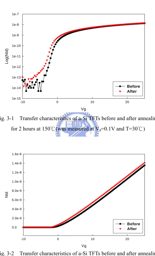
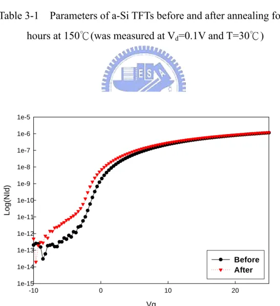
(31) Chapter 3 Result and Discussion. 3.1. Electrical Analysis Figure 3-1 shows transfer characteristics of a-Si TFTs (log (NId)-Vg) before and. after annealing in supercritical fluids treatment system for 2 hours at 150℃. TFTs had a gate width of 20μm and a gate length of 10μm. The transfer characteristics were measured at a drain voltage 0.1V and temperature was 30℃. After annealing, subthreshold swing was the same as before annealing. This means that deep states in the channel region (amorphous silicon) were alike while it was been heated 2 hours at 150℃. Especially, off current was increase after annealing. Figure 3-2 shows transfer characteristics of a-Si TFTs (NId-Vg) before and after annealing in supercritical fluids treatment system for 2 hours at 150℃. From slope of the curve, we observed that before and after annealing the mobility were similar. However, threshold voltage showed slight improvement after annealing. Table 3-1 shows parameters (field-effect mobility, subthreshold swing and threshold voltage) of a-Si TFTs before and after annealing in supercritical fluids treatment system for 2 hours at 150℃. TFTs had a gate width of 20μm and a gate length of 10μm. The transfer characteristics were measured at a drain voltage 0.1V and temperature was 30℃. Here we used random sampling and obtained 3 series of measured results. In these result, it could observed that mobility was slight decrease after annealing. However, threshold voltage and subthreshold swing showed slight improvement after annealing. Figure 3-3 shows transfer characteristics of a-Si TFTs (log (NId)-Vg) before and after annealing in supercritical fluids treatment system for 2 hours at 150℃. TFTs had a gate width of 20μm and a gate length of 10μm. The transfer characteristics were 19.
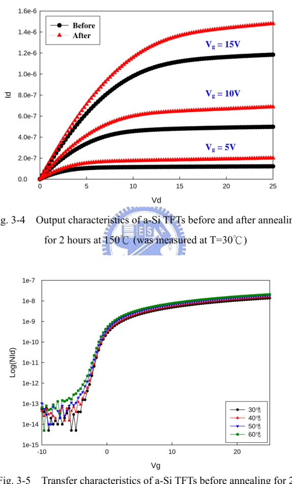
(32) measured at a drain voltage 10V and temperature was 30℃. Subthreshold swing was the same whatever before or after annealing. But, the off current increased after annealing in comparison with before annealing. Figure 3-4 shows output characteristics of a-Si TFTs before and after annealing in supercritical fluids treatment system for 2 hours at 150℃. TFTs had a gate width of 20μm and a gate length of 10μm. The output characteristics were measured in temperature of 30 ℃ . It was been observed that drain current increased after annealing. Figure 3-5 shows transfer characteristics of a-Si TFTs before annealing in supercritical fluids treatment system for 2 hours at 150℃. TFTs had a gate width of 20μm and a gate length of 10μm. The transfer characteristics were measured at a drain voltage 0.1V and temperature 30℃~60℃. Figure 3-6 shows transfer characteristics of a-Si TFTs after annealing in supercritical fluids treatment system for 2 hours at 150℃. TFTs had a gate width of 20μm and a gate length of 10μm. The transfer characteristics were measured at a drain voltage 0.1V and temperature 30℃~60℃. Figure 3-7 shows transfer characteristics of a-Si TFTs before annealing in supercritical fluids treatment system for 2 hours at 150℃. TFTs had a gate width of 20μm and a gate length of 10μm. The transfer characteristics were measured at a drain voltage 10V and temperature 30℃~60℃. Figure 3-8 shows transfer characteristics of a-Si TFTs after annealing in supercritical fluids treatment system for 2 hours at 150℃. TFTs had a gate width of 20μm and a gate length of 10μm. The transfer characteristics were measured at a drain voltage 10V and temperature 30℃~60℃. Figure 3-9 shows temperature activation of the drain-source current of the only annealing 2 hours at 150℃ sample (Figure 3-6) for different gate voltages. From the slope of Figure 3-9, we could extract the activation energy. Figure 3-10 shows activation energy vs. gate voltage for the samples which before and after annealing in supercritical fluids treatment system for 2 hours at 150℃. TFTs had a gate width of 20μm and a gate length of 10μm. For gate voltages from -6V to 6V, the activation energy (Ea) before and after annealing was the same. 20.
(33) Therefore, defect states before and after annealing were similarity. Figure 3-11 shows density of states (DOS) vs. trap state energy (Et) for the samples which before and after annealing in supercritical fluids treatment system for 2 hours at 150℃. TFTs had a gate width of 20μm and a gate length of 10μm. Where trap state energy (Et) was the needful energy which electron in the trap of the amorphous silicon band gap jumped to conduction band (EC). It was observed that density of states (DOS) before and after annealing was almost the same. That is to say defect states before and after annealing were similarity. Figure 3-12 shows transfer characteristics of a-Si TFTs (log (NId)-Vg) before and after H2O passivation for 2 hours at 150℃. TFTs had a gate width of 20μm and a gate length of 10μm. The transfer characteristics were measured at a drain voltage 0.1V (and 5V) and temperature 30℃. Subthreshold swing, threshold voltage and mobility were serious decrease after H2O passivation in comparison with before passivation. Figure 3-13 shows transfer characteristics of a-Si TFTs (NId-Vg) before and after H2O passivation for 2 hours at 150℃. Table 3-2 shows parameters (field-effect mobility, subthreshold swing and threshold voltage) of a-Si TFTs before and after H2O passivation for 2 hours at 150℃. TFTs had a gate width of 20μm and a gate length of 10μm. The transfer characteristics were measured at a drain voltage 0.1V (and 5V) and temperature was 30℃. Here we used random sampling and obtained 3 series of measured results. In these result, it could observed that mobility, threshold voltage and subthreshold swing showed serious decrease after H2O passivation. Figure 3-14 shows transfer characteristics of a-Si TFTs (log (NId)-Vg) before and after H2O passivation for 2 hours at 150℃. TFTs had a gate width of 20μm and a gate length of 10μm. The transfer characteristics were measured at a drain voltage 10V (and 20V) and temperature was 30℃. We observed that all parameters of a-Si TFT were also serious decrease. Figure 3-15 shows output characteristics of a-Si TFTs before and after H2O passivation for 2 hours at 150℃. TFTs had a gate width of 20μm and a gate length of 21.
(34) 10μm. The output characteristics were measured at temperature was 30℃. Current crowding phenomenon was been observed after H2O passivation because of source and drain metals were been oxidation seriously by H2O. Then, resistance was increase. Figure 3-16 shows transfer characteristics of a-Si TFTs (log (NId)-Vg) before and after SCCO2 fluid interfuse H2O passivation for 2 hours at 150℃. TFTs had a gate width of 20μm and a gate length of 10μm. The transfer characteristics were measured at a drain voltage 0.1V and temperature was 30℃. After SCCO2 fluid interfuse H2O passivation, subthreshold swing was better than original sample. This means that deep states in the channel region (amorphous silicon) was been extensive decrease. Especially, off current was lower than that of original sample. Because of back channel was repaired by oxygen atoms from SCCO2 fluid interfuse H2O. Figure 3-17 shows transfer characteristics of a-Si TFTs (NId-Vg) before and after SCCO2 fluid interfuse H2O passivation for 2 hours at 150℃. From slope of the curve, we observed that mobility increased after SCCO2 fluid interfuse H2O passivation. In addition, threshold voltage was extensive improvement after SCCO2 fluid interfuse H2O passivation. Table 3-3 shows parameters (field-effect mobility, subthreshold swing and threshold voltage) of a-Si TFTs before and after SCCO2 fluid interfuse H2O passivation for 2 hours at 150℃. TFTs had a gate width of 20μm and a gate length of 10μm. The transfer characteristics were measured at a drain voltage 0.1V and temperature was 30℃. Here we used random sampling and obtained 3 series of measured results. In these result, it could observed that mobility, threshold voltage and subthreshold swing showed extensive improvement after SCCO2 fluid interfuse H2O passivation. Figure 3-18 shows transfer characteristics of a-Si TFTs (log (NId)-Vg) before and after SCCO2 fluid interfuse H2O passivation for 2 hours at 150℃. TFTs had a gate width of 20μm and a gate length of 10μm. The transfer characteristics were measured at a drain voltage 10V and temperature of 30℃. We observed that all 22.
(35) parameters of a-Si TFT were also improvement. Figure 3-19 shows output characteristics of a-Si TFTs before and after SCCO2 fluid interfuse H2O passivation for 2 hours at 150℃. TFTs had a gate width of 20μm and a gate length of 10μm. The output characteristics were measured at temperature of 30℃. It was been observed that drain current was increase after SCCO2 fluid interfuse H2O passivation. Figure 3-20 shows transfer characteristics of a-Si TFTs before SCCO2 fluid interfuse H2O passivation for 2 hours at 150℃. TFTs had a gate width of 20μm and a gate length of 10μm. The transfer characteristics were measured at a drain voltage 0.1V and temperature 30℃~60℃. Figure 3-21 shows transfer characteristics of a-Si TFTs after SCCO2 fluid interfuse H2O passivation for 2 hours at 150℃. TFTs had a gate width of 20μm and a gate length of 10μm. The transfer characteristics were measured at a drain voltage 0.1V and temperature 30℃~60℃. Figure 3-22 shows transfer characteristics of a-Si TFTs before SCCO2 fluid interfuse H2O passivation for 2 hours at 150℃. TFTs had a gate width of 20μm and a gate length of 10μm. The transfer characteristics were measured at a drain voltage 10V and temperature 30℃ ~60℃. Figure 3-23 shows transfer characteristics of a-Si TFTs after SCCO2 fluid interfuse H2O passivation for 2 hours at 150℃. TFTs had a gate width of 20μm and a gate length of 10μm. The transfer characteristics were measured at a drain voltage 10V and temperature 30℃~60℃. Figure 3-24 shows activation energy vs. gate voltage for the samples which before and after SCCO2 fluid interfuse H2O passivation for 2 hours at 150℃. TFTs had a gate width of 20μm and a gate length of 10μm. For gate voltages from -6V to -2V, the activation energy (Ea) after SCCO2 fluid interfuse H2O passivation was higher than before SCCO2 fluid interfuse H2O passivation. Because of a-Si TFT back channel was repaired. The mechanism of back channel was discussed in the chapter 3.3. For gate voltages from -2V to 2V, the activation energy (Ea) after SCCO2 fluid interfuse H2O passivation was lower than before SCCO2 fluid interfuse H2O passivation. That is deep states were decrease after SCCO2 fluid interfuse H2O 23.
(36) passivation. For gate voltages from 2V to 6V, the activation energy (Ea) after SCCO2 fluid interfuse H2O passivation was lower than before SCCO2 fluid interfuse H2O passivation. That is tail states were also decrease after SCCO2 fluid interfuse H2O passivation. Figure 3-25 shows density of states (DOS) vs. trap state energy (Et) for the samples which before and after SCCO2 fluid interfuse H2O passivation for 2 hours at 150℃. TFTs had a gate width of 20μm and a gate length of 10μm. Where trap state energy (Et) was the needful energy which electron in the trap of the amorphous silicon band gap jumped to conduction band (EC). It was observed that deep states were largely decreased. That is to say defect states were effectual degradation after SCCO2 fluid interfuse H2O passivation.. 3.2. Material Analysis. From experiment result of chapter 3.1, we conjecture that defect states are decreasing because of the dangling bonds can be terminated by oxygen atoms provided from H2O. In order to demonstrate the incorporation of oxygen in silicon films by the supercritical fluid passivation interfuse H2O. In this section, we use fourier transform infrared spectroscopy (FTIR) to observe the change of intensity of Si-O bonding. In addition, contact angle and thermal desorption spectroscopy (TDS) are also been use. Figure 3-26 shows the optical absorption spectra after passivation 2 hours. There was no increment in the Si-H absorption peak within wavelength 2000 cm-1 ~ 2200 cm-1 after the H2O and supercritical fluids passivation. However, the S-O absorption peak (~ 1080 cm-1) was been observed, and there was increment in H2O and supercritical fluids samples compared with only annealing treatment. Figure 3-27 shows the optical absorption spectra after passivation 2 hours and then hot plate baking 1 hour at 200℃. The same as before hot plate baking (Figure. 24.
(37) 3-26), there was no increment in the Si-H absorption peak within wavelength 2000 cm-1 ~ 2200 cm-1 after the H2O and supercritical fluids passivation. However, the S-O absorption peak (~ 1080 cm-1) was observed, and there was increment in H2O and supercritical fluids samples compared with only annealing treatment. From figure 3-26, figure 3-27 and above discussions, it could be confirmed that oxygen atoms dissociated from H2O and supercritical CO2 fluid interfuse H2O would only have the role of terminating the dangling bonds locally. The present passivation by H2O and supercritical CO2 fluid interfuse H2O will be useful for the reduction of the defects in the silicon films for a-Si TFTs fabrication processing. During H2O and supercritical CO2 fluid interfuse H2O passivation, a large number of polar H2O molecules would be absorbed in polycrystalline silicon thin film. Therefore, the analysis of thermal desorption spectroscopy (TDS) for moisture, M/e (mass-to-charge ratio) = 18 peak, is shown below. Figure 3-28 shows the thermal desorption spectroscopy (TDS) after passivation 2 hours. It is apparent that the quantity of moisture in polycrystalline silicon thin films is arising greatly after H2O passivation. However, the content of moisture is almost intact, even less than the only annealing sample, after SCCO2 fluids process mixed with H2O. This reason is supercritical CO2 fluids possess the high density property like liquid, so it can transport more supercritical fluid than liquid. And supercritical CO2 has diffusivity greater than liquid, allowing for rapid transport properties. Besides, the absence of surface tension provides for excellent mass transport into micro-porous matrices. Figure 3-29 shows the thermal desorption spectroscopy (TDS) after passivation 2 hours and then hot plate baking 1 hour at 200℃. It is apparent that the quantity of moisture in polycrystalline silicon thin films is almost the same as only annealing sample after H2O passivation and SCCO2 fluids passivation mixed with H2O. Because of these samples was heating 1 hour after passivation. For above discussion, SCCO2 fluids passivation mixed with H2O maked devices performance better. Additionally, the absorbed moisture in silicon thin films was also decreased after supercritical fluids passivation. 25.
(38) Material has hydrophobic resin or hydrophilic resin. When DI water drop in hydrophobic resin, the value of contact angle is larger. After some treatment or on another material of hydrophilic resin, the value of contact angle is reduced (Figure 3-30). In other words, material has hydrophobic resin then the value of contact angle is larger. Material has hydrophilic resin then the value of contact angle is smaller. Table 3-4 shows contact angle of polycrystalline silicon thin films after passivation 2 hours. Lower row was after passivation 2 hours and then baking 1 hour at 200℃. Upper row was after passivation 2 hours without baking 1 hour. From experimental result, the contact angle of only annealing samples was slight decrease in contradistinction to original polycrystalline silicon thin films. The slight decrease in contact angle was native oxide on the surface after annealing. However, the contact angle of passivation by H2O and SCCO2 fluids mixed with H2O was heavily reduced compared with original polycrystalline silicon thin films and only annealing samples. Because these samples surfaces were been oxidation by moisture. According to above results, it was been confirmed that the silicon bonds would be terminated by oxygen atoms provided from H2O.. 3.3. Mechanism. In this chapter, we will discuss density of states (DOS) in the amorphous silicon and back channel effect in the a-Si TFTs. 1. Density of states (DOS) in the amorphous silicon In a-Si film, defects are uniformly distributed over the film volume. The crystalline order is lost within a distance of the order of the lattice parameter. This results in the modification of band structure. The energy gap of a-Si is 1.5eV, compared to 1.1 eV of single crystal silicon. The lack of a long-range order also implies that some of the bonds are unsaturated, that is, dangling. In practice, a. 26.
(39) concentration of dangling bonds in the material is not avoidable. Reconstructed bonds can form among dangling bonds. Both dangling and reconstructed bonds give rise to electronic energy levels in the energy gap, and the dangling bond states are believed to be located near mid-gap [35] (Figure 3-31). Other gap states can be introduced purely as a consequence of the random fluctuations of the crystalline potential. These states (disorder-induced localized states) are located at energies close to the conduction and valence bands, and they constitute the so-called band tails [35] (Figure 3-31). As a results, the energy gap is occupied with a continuum of states, and -3. -1. is described by the DOS function N(E), which is expressed in cm eV . The a-Si:H TFT operation theory [36] (Figure 3-32) is very different from crystal silicon MOSFET. When no voltage is applied, the energy bands are closed to the flat band condition. If a gate voltage, which is positive but less than threshold voltage, the Fermi level moves through the deep states, which are occupied. Meanwhile, some space charges locate in the tail band and the occupancy of these states is low, since they are above the Fermi level. Thus, the deep states dominate the total space charge. The small fraction of the band tail electrons above the conduction band mobility edge makes the increasing of source-drain current. The space charges in the deep states increase in proportion to the increase in the gate voltage, but the current increases exponentially as the band bending increases. Above the threshold voltage, the space charge in the band tail states exceeds the space charge in the deep states, even though the Fermi level is still below the tail states. Now, both the total space charge and the source-drain current increase linearly with the applied gate voltage and we have a well define filed effect mobility. The mobility is thermally activated with an activation energy given by the width of the tail states, not by EC-EF. As mentioned above, we know that the Fermi level shift with the gate voltage is strongly dependent on the density of states (DOS). At high density of states more carriers must be induced in order to fill the states from EF upward. Therefore, it is necessary to apply higher gate voltage in order to induce more carriers in the channel. On the contrary, when the density of states is low, the states from EF upward are 27.
(40) easily filled at low concentration of the induced charge and the Fermi level is easily shifted at low gate voltages. From correlation between the DOS and the gate voltage allows obtaining the shape of the density of states by studying the dependence of Ea vs. Vg. The information on DOS shape is important for understanding the physical mechanisms responsible for the device behaviors. The DOS shape is related to the threshold voltage, subthreshold swing, and field effect mobility of the TFTs.. 2. Back channel effect in the a-Si TFTs Figure 3-33 depicts the leakage characteristics of the TFT [37]. Here, we identify three distinguishable regions, which are characterized by ohmic conduction, front channel conduction and conduction at the back interface. The relative dominance of each mechanism is determined by bias conditions and device geometry, and is elaborated in the reference paper [37]. Here, we discuss the reverse subthreshold region (back channel region). When we apply low positive (or negative) gate voltages, the drain-source current changes exponentially with the gate-source voltage [37]. This region is known as the subthreshold region, either for forward and reverse regimes of operation. At low positive VGS, the accumulation of electrons at the front a-Si:H / a-SiNx:H interface is responsible for subthreshold conduction, whereby the TFT’s drain-source current varies exponentially with the gate voltage. The extension of the band bending at the interface into the bulk a-Si:H layer provides a low concentration of free electrons, which in turn enables conduction by virtue of diffusion. As the gate voltage is decreased to zero and to low negative values, this accumulation of electrons at the front interface decreases only to leave behind electrons at the back a-Si:H / a-SiNx:H interface, which now become responsible for the reverse subthreshold behavior (conduction at the back interface). As the gate voltage is decreased further to high negative VGS, there is a growing accumulation of holes at the front interface. The. 28.
(41) conduction of this front hole channel is responsible for the exponential increase in the current at high negative gate and high positive drain voltages (Figure 3-33). The current is limited by field-enhanced generation of holes at the gate-drain overlap vicinity by virtue of the Poole-Frenkel effect. At low negative VGS, the presence of electrons at the back interface and the extended band bending in the bulk a-Si:H provides a conduction path for leakage [37]. The density of electrons at the back interface is dependent on the applied gate voltage. An increase in the negative gate voltage decreases band bending and thus the electron density at this interface. Therefore, the charge at the back interface can be reduced to zero from its initial negative value (electrons) and can then become positive (holes) by virtue of the negative gate voltage. Figure 3-34 shows the band diagram for an arbitrary cross section of the TFT in the middle of the channel, which illustrates the accumulation of electrons at the back interface. At low negative VGS, Gauss’ Law yields for the electric field (ESi) in the a-Si:H at the back interface. E Si =. q 2 D ssb. ε Si. (ψ Sb 0 − ψ Sb ). (3-1). Here, q denotes the elementary charge, ε Si the dielectric constant of a-Si:H,. DSSb the density of interface states, ψ Sb the band bending, and ψ Sb 0 the no-voltage band bending at the back interface. The applied voltage Va can be written as. Va = ψ Sf + Vi + VFB. (3-2). Where Vi is the voltage drop over the gate insulator and. VFB = φM − χ S −. ECFn q. (3-3). Here, φ M is the gate metal work function, χ S the electron affinity in a-Si:H, and ECFn the difference between the conduction band edge and the intrinsic Fermi-level in a-Si:H. Gauss’ Law for the electric field (ESS) at the front interface gives. 29.
(42) C iVi − ε Si E SS = q 2 D SSf (ψ Sf − ψ Sf 0 ). (3-4). Where Ci is the gate dielectric capacitance per unit area, DSSf is the density of interface states, ψ Sf is the band bending at the front interface and ψ Sf 0 is the zero-voltage band bending at the front interface. Reference paper [37], we can get the following equation. Va − V FB =. q 2 D SSf Ci. (ψ. Sf. − ψ Sf 0 ) + ψ Sf +. ε Si Ci. 2. 2 qN tpVtp ψ Sf / Vtp ⎛ q 2 D SSb ⎞ (ψ Sb 0 − ψ Sb )⎟⎟ + e × ⎜⎜ ε Si ⎝ ε Si ⎠. (3-5). At low negative VGS, the trapped carriers at the interface are much higher than those trapped in the donor-like tail states. The reduces above equation to. Va − V FB ≈. q 2 DSSf Ci. (ψ. Sf. − ψ Sf 0 ) + ψ Sf. q 2 DSSb (ψ Sb 0 − ψ Sb ) + Ci. (3-6). Above equation shows the effect of the applied voltage on the band bending at the two interfaces. Then, we substitute below equation into above equation. The voltage drop (VSi) across the a-Si:H layer is. V Si ≈ ψ Sf − ψ Sf 0 =. q 2 D SSb. ε Si. (ψ Sb 0 − ψ Sb )t Si. (3-7). Yields. Va − V FB = a b (Vb 0 − ψ Sb ). (3-8). Where. q 2 DSSb ab ≈ Ci. ⎛ q 2 Dssf ⎜1 + ⎜ CS ⎝. ⎞ ⎟ ⎟ ⎠. Vb 0 ≈ ψ Sb 0 CS =. ε Si t Si. The current density Jch in the back channel due to the presence of free electrons, 30.
(43) is. J ch = n free μ n. ∂E fn. (3-9). ∂x. Where nfree is the density of free electrons, μ n is the effective mobility of electrons in the a-Si:H bulk, Efn is the quasi Fermi level of electrons, and x is the position. The density of free electrons can be written as. n free = N C e. −. ECFn VT. ψ. e. VT. (3-10). Where NC is the density of free carriers at the conduction band edge and VT is the thermal voltage. Integrating Jch over the channel thickness yields the total current at the back interface (IBC), as δ. ∂E fn. 0. ∂x. I BC = W ∫ n free μ n. dy. (3-11). Here, δ is the thickness of the electron accumulation layer close to the back interface. Then, calculates above equation and refers to paper [37], we can get the following equation VGS −Vtb. W S +γ V I BC = I 0 B e r n DS L Vq q 2 DSSb ⎛ q 2 DSSf ⎜1 + Sr = ≈ ab Ci ⎜⎝ CS Vtb ≈ abVb 0 ≈. I0B =. (3-12). ⎞ ⎟VT ⎟ ⎠. Sr ψ Sb 0 VT. (3-13). (3-14). − ECFn VT. qN C e μn Sr E nd Vq. (3-15). Where, Sr denotes the reverse sub threshold slope and γ n is a fitting parameter. Comparing the slopes of the current-voltage characteristics in the reverse and forward subthreshold regimes, the density of states at the back and front interfaces can. 31.
(44) be obtained. However, the front interface has an interface state density that is smaller by a factor of three only compared to the back interface.. q 2 DSSb Sr = ≈ ab Ci Vq. ⎛ q 2 DSSf ⎜1 + ⎜ CS ⎝. ⎞ ⎟VT ⎟ ⎠. From above equation, we also know that the density of back interface states (Dssb) is lesser, reverse subthreshold swing (Sr) is smaller.. 3.4. Summary. In this chapter, we confirm that after the supercritical fluid passivation achieve better device performances, including the on-current, the off-current, the threshold voltage and the subthreshold swing, and also better filed effect mobility. In addition, back channel is also repaired by supercritical fluid passivation. These improvements are attributed to the oxygen atoms passivation of the dangling bonds and it is observed by material analysis (i.e. FTIR, TDS and Contact angle). These mean that density of defect states in the channel region (amorphous silicon) are decreased after supercritical fluid passivation interfuse H2O.. 32.
(45) 1e-7 1e-8 1e-9. Log(NId). 1e-10 1e-11 1e-12 1e-13. Before After. 1e-14 1e-15 -10. 0. 10. 20. Vg. Fig. 3-1 Transfer characteristics of a-Si TFTs before and after annealing for 2 hours at 150℃(was measured at Vd=0.1V and T=30℃). 1.6e-8 1.4e-8 1.2e-8. NId. 1.0e-8 8.0e-9 6.0e-9 4.0e-9 2.0e-9. Before After. 0.0. -10. 0. 10. 20. Vg. Fig. 3-2 Transfer characteristics of a-Si TFTs before and after annealing for 2 hours at 150℃(was measured at Vd=0.1V and T=30℃) 33.
(46) Device name. W/L=20/10. Mobility (cm2/VS). S.S. (V/dec.). Vth (V). Sample 1. Before. 0.4018. 2.0616. 2.6603. After. 0.3774. 1.7849. 1.5966. Before. 0.4020. 2.0539. 2.2678. After. 0.3938. 1.8941. 0.8000. Before. 0.4032. 2.0773. 2.7078. After. 0.3738. 1.7901. 1.1619. Sample 2. Sample 3. Table 3-1 Parameters of a-Si TFTs before and after annealing for 2 hours at 150℃(was measured at Vd=0.1V and T=30℃). 1e-5 1e-6 1e-7. Log(NId). 1e-8 1e-9 1e-10 1e-11 1e-12 1e-13. Before After. 1e-14 1e-15 -10. 0. 10. 20. Vg. Fig. 3-3 Transfer characteristics of a-Si TFTs before and after annealing for 2 hours at 150℃ (was measured at Vd=10V and T=30℃) 34.
(47) 1.6e-6. Before After. 1.4e-6. Vg = 15V 1.2e-6. Id. 1.0e-6. Vg = 10V. 8.0e-7 6.0e-7 4.0e-7. Vg = 5V 2.0e-7 0.0 0. 5. 10. 15. 20. 25. Vd. Fig. 3-4 Output characteristics of a-Si TFTs before and after annealing for 2 hours at 150℃ (was measured at T=30℃). 1e-7 1e-8 1e-9. Log(NId). 1e-10 1e-11 1e-12 1e-13 30度 40度 50度 60度. 1e-14 1e-15 -10. 0. 10. 20. Vg. Fig. 3-5 Transfer characteristics of a-Si TFTs before annealing for 2 hours at 150℃(was measured at Vd=0.1V and T=30℃~60℃) 35.
(48) 1e-7 1e-8 1e-9. Log(NId). 1e-10 1e-11 1e-12 1e-13. 30度 40度 50度 60度. 1e-14 1e-15 -10. 0. 10. 20. Vg. Fig. 3-6 Transfer characteristics of a-Si TFTs after annealing for 2 hours at 150℃(was measured at Vd=0.1V and T=30℃~60℃). 1e-5 1e-6 1e-7. Log(NId). 1e-8 1e-9 1e-10 1e-11 1e-12 30度 40度 50度 60度. 1e-13 1e-14 1e-15 -10. 0. 10. 20. Vg. Fig. 3-7 Transfer characteristics of a-Si TFTs before annealing for 2 hours at 150℃(was measured at Vd=10V and T=30℃~60℃) 36.
(49) 1e-5 1e-6 1e-7. Log(NId). 1e-8 1e-9 1e-10 1e-11 1e-12 30度 40度 50度 60度. 1e-13 1e-14 1e-15 -10. 0. 10. 20. Vg. Fig. 3-8 Transfer characteristics of a-Si TFTs after annealing for 2 hours at 150℃(was measured at Vd=10V and T=30℃~60℃). -16. -18. Log (NId). -20. -22. -24. -26. -28 0.00295 0.00300 0.00305 0.00310 0.00315 0.00320 0.00325 0.00330 0.00335. 1/T. Fig. 3-9 Temperature activation of the drain-source current of the only annealing 2 hours at 150℃ sample (Fig. 3-6) for different gate voltages. 37.
(50) 0.8. Before After. Ea. 0.6. 0.4. 0.2. 0.0 -6. -4. -2. 0. 2. 4. 6. Vg. Fig. 3-10 Activation energy vs. gate voltage for the samples before and after annealing in supercritical fluids treatment system (2 hours, 150℃). 1e+19. Density of states. Before After. 1e+18. 1e+17. 1e+16 0.1. 0.2. 0.3. 0.4. 0.5. 0.6. 0.7. Et. Fig. 3-11 Density of states (DOS) vs. Et for the samples before and after annealing in supercritical fluids treatment system (2 hours, 150℃) 38.
(51) 1e-7 1e-8 1e-9. Log(NId). 1e-10 1e-11 1e-12 1e-13. Before(Vd=0.1V) After(Vd=5V). 1e-14 1e-15 -10. 0. 10. 20. Vg. Fig. 3-12 Transfer characteristics of a-Si TFTs before and after H2O passivation for 2 hours at 150℃(was measured at linear region, T=30℃). 1.6e-8 1.4e-8 1.2e-8. Log(NId). 1.0e-8 8.0e-9 6.0e-9 4.0e-9 2.0e-9. Before(Vd=0.1V) After(Vd=5V). 0.0. -10. 0. 10. 20. Vg. Fig. 3-13 Transfer characteristics of a-Si TFTs before and after H2O passivation for 2 hours at 150℃(was measured at linear region, T=30℃) 39.
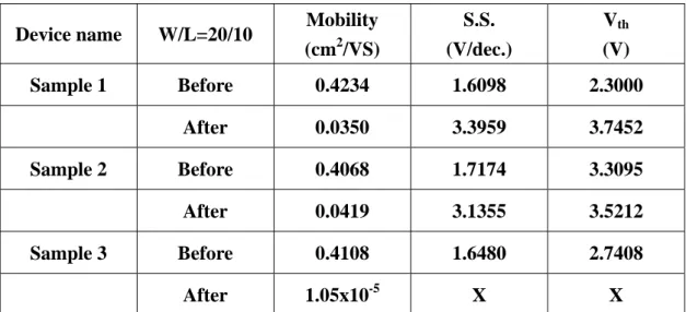
(52) Device name. W/L=20/10. Mobility (cm2/VS). S.S. (V/dec.). Vth (V). Sample 1. Before. 0.4234. 1.6098. 2.3000. After. 0.0350. 3.3959. 3.7452. Before. 0.4068. 1.7174. 3.3095. After. 0.0419. 3.1355. 3.5212. Before. 0.4108. 1.6480. 2.7408. After. 1.05x10⁻⁵. X. X. Sample 2. Sample 3. Table 3-2 Parameters of a-Si TFTs before and after H2O passivation for 2 hours at 150℃(was measured at linear region and T=30℃). 1e-5 1e-6 1e-7. Log(NId). 1e-8 1e-9 1e-10 1e-11 1e-12 1e-13. Before(Vd=10V) After(Vd=20V). 1e-14 1e-15 -10. 0. 10. 20. Vg. Fig. 3-14 Transfer characteristics of a-Si TFTs before and after H2O passivation for 2 hours at 150℃ (was measured at sat. region, T=30℃) 40.
(53) 1.6e-6. Before After. 1.4e-6. Vg=5V(Before) Vg=10V(Before) Vg=15V(Before) Vg=10V(After) Vg=15V(After) Vg=20V(After). 1.2e-6. Id. 1.0e-6 8.0e-7 6.0e-7 4.0e-7 2.0e-7 0.0 0. 5. 10. 15. 20. 25. Vd. Fig. 3-15 Output characteristics of a-Si TFTs before and after H2O passivation for 2 hours at 150℃ (was measured at T=30℃). 1e-7 1e-8 1e-9. Log(NId). 1e-10 1e-11 1e-12 1e-13. Before After. 1e-14 1e-15 -10. 0. 10. 20. Vg. Fig. 3-16 Transfer characteristics of a-Si TFTs before and after SCCO2 passivation for 2 hours at 150℃. (was measured at Vd=0.1V and T=30℃) 41.
(54) 1.8e-8 1.6e-8 1.4e-8. Log(NId). 1.2e-8 1.0e-8 8.0e-9 6.0e-9 4.0e-9 2.0e-9. Before After. 0.0 -10. 0. 10. 20. Vg. Fig. 3-17 Transfer characteristics of a-Si TFTs before and after SCCO2 passivation for 2 hours at 150℃. (was measured at Vd=0.1V and T=30℃). Device name. W/L=20/10. Mobility (cm2/VS). S.S. (V/dec.). Vth (V). Sample 1. Before. 0.4265. 2.0447. 2.8018. After. 0.4375. 1.3272. 0.4224. Before. 0.4249. 1.9111. 1.6530. After. 0.4358. 1.6278. 0.2700. Before. 0.4230. 1.8460. 1.1170. After. 0.4390. 1.4542. 0.2673. Sample 2. Sample 3. Table 3-3 Parameters of a-Si TFTs before and after SCCO2 passivation for 2 hours at 150℃(was measured at Vd=0.1V and T=30℃). 42.
(55) 1e-5 1e-6 1e-7. Log(NId). 1e-8 1e-9 1e-10 1e-11 1e-12 1e-13. Before After. 1e-14 1e-15 -10. 0. 10. 20. Vg. Fig. 3-18 Transfer characteristics of a-Si TFTs before and after SCCO2 passivation for 2 hours at 150℃. (was measured at Vd=10V and T=30℃). 1.6e-6. Vg = 15V. Before After. 1.4e-6 1.2e-6. Id. 1.0e-6. Vg = 10V. 8.0e-7 6.0e-7 4.0e-7. Vg = 5V. 2.0e-7 0.0 0. 5. 10. 15. 20. 25. Vd. Fig. 3-19 Output characteristics of a-Si TFTs before and after SCCO2 passivation for 2 hours at 150℃ (was measured at T=30℃) 43.
(56) 1e-7 1e-8 1e-9. Log(NId). 1e-10 1e-11 1e-12 1e-13. 30度 40度 50度 60度. 1e-14 1e-15 -10. 0. 10. 20. Vg. Fig. 3-20 Transfer characteristics of a-Si TFTs before SCCO2 passivation for 2 hours at 150℃(measured at Vd=0.1V, T=30℃~60℃). 1e-7 1e-8 1e-9. Log(NId). 1e-10 1e-11 1e-12 1e-13. 30度 40度 50度 60度. 1e-14 1e-15 -10. 0. 10. 20. Vg. Fig. 3-21 Transfer characteristics of a-Si TFTs after SCCO2 passivation for 2 hours at 150℃(measured at Vd=0.1V, T=30℃~60℃) 44.
(57) 1e-5 1e-6 1e-7. Log(NId). 1e-8 1e-9 1e-10 1e-11 1e-12 30度 40度 50度 60度. 1e-13 1e-14 1e-15 -10. 0. 10. 20. Vg. Fig. 3-22 Transfer characteristics of a-Si TFTs before SCCO2 passivation for 2 hours at 150℃(measured at Vd=10V, T=30℃~60℃). 1e-5 1e-6 1e-7. Log(NId). 1e-8 1e-9 1e-10 1e-11 1e-12 30度 40度 50度 60度. 1e-13 1e-14 1e-15 -10. 0. 10. 20. Vg. Fig. 3-23 Transfer characteristics of a-Si TFTs after SCCO2 passivation for 2 hours at 150℃(measured at Vd=10V, T=30℃~60℃) 45.
(58) 1.2. Before After. 1.0. Ea. 0.8. 0.6. 0.4. 0.2. 0.0 -6. -4. -2. 0. 2. 4. 6. Vg. Fig. 3-24 Activation energy vs. gate voltage for the samples before and after SCCO2 fluid interfuse H2O passivation (2 hours, 150℃). 1e+19. Density of states. Before After. 1e+18. 1e+17. 1e+16 0.1. 0.2. 0.3. 0.4. 0.5. 0.6. 0.7. Et. Fig. 3-25 Density of states (DOS) vs. Et for the samples before and after SCCO2 fluid interfuse H2O passivation (2 hours, 150℃) 46.
(59) 0.04. Intensity. 0.02. 0.00. Anneal H2O. -0.02. SCCO2 / Propyl alcohol+H2O 500. 1000. 1500. 2000. 2500. Wavenumber. Fig. 3-26 Infrared absorption spectra after passivation 2 hours. 0.04 0.03. Intensity. 0.02 0.01 0.00 -0.01 Anneal H2O. -0.02. SCCO2 / Propyl alcohol+H2O -0.03 500. 1000. 1500. 2000. 2500. Wavenumber. Fig. 3-27 Infrared absorption spectra after passivation 2 hours and then hot plate baking 1 hour 47.
(60) Annealing H2O. 6e-8. SCCO2/H2O+Propyl alcohol. Intensity. 5e-8. 4e-8. 3e-8. 2e-8. 80. 100. 120. 140. 160. 180. 200. Temperature. Fig. 3-28 Thermal desorption spectroscopy after passivation 2 hours. Annealing H2O. 6e-8. SCCO2/H2O+Propyl alcohol. Intensity. 5e-8. 4e-8. 3e-8. 2e-8. 80. 100. 120. 140. 160. 180. 200. Temperature. Fig. 3-29 Thermal desorption spectroscopy after passivation 2 hours and then hot plate baking 1 hour at 200℃ 48.
(61) α Substrates. Fig. 3-30 Contact angle measurement. SCCO2 / H2O. Poly - Si (without any treatment). Annealing. H2O. +Propyl alcohol. Before (hot plate) Baking. 48.1. 38. 5. 17.4. After (hot plate) Baking. 40.9. 40.7. 7.5. 20.9. Table 3-4 Contact angle after passivation. 49.
(62) Fig. 3-31 Density of states (DOS) in the amorphous silicon. Gate. SiNx. a-Si. Gate. Vg=VFB. SiNx. a-Si. Gate. EC Ei EF EV. a-Si. Vg>VT. VFB<Vg<VT. EFM. SiNx. EFM. EC. EC. EF. EF. EV. EV EFM. EC. EC. Ei EF. EF Ei. EC EF. Vg=VFB. VFB<Vg<VT. EV. Ei Vg>VT. EV. EV. Fig. 3-32 Schematic illustration of the basic operation of the a-Si TFT 50.
(63) Front channel Poole-Frenkel. 1x10⁻⁶. emission. ID(A). 1x10⁻⁸. Sub-threshold. Above Threshold. Front channel VDS = 20 V. 1x10. Forward. -10. Sub-threshold. VDS = 10 V. (Front channel). 1x10-12 Reverse Sub-threshold (Back channel) 1x10. -14. -20. -15. -10. -5. 0. 5. 10. 15. 20. VGS (V). Fig. 3-33 Drain-source current vs. gate-source voltage of the a-Si TFT. qVi. EFM qVa. qΨsf. Ei. EC. qΨsb. EFS. EFS Ess. EV Esi. Gate. SiNx:H. a-Si:H. Air. Fig. 3-34 Band diagram for a cross section in the channel area of the a-Si TFT 51.
(64) Chapter 4 Conclusion. Amorphous silicon thin film transistors (a-Si TFTs) have been widely applied to fabrication of liquid crystal flat-panel display. Plasma enhancement chemical vapor deposition (PECVD) has been used for fabrication of a-Si TFTs at low temperatures. Inevitable amorphous silicon films among deposition can have electrically active defect states due to dangling bonds and lattice disorder. The defects reduce electrical current due to trapping carriers. One of most important problems on fabrication of a-Si TFTs is the reduction of densities of those defect states. In this thesis, we report fabrication of a-Si TFTs using defect reduction of supercritical fluid passivation interfuse H2O. This method of the defect reduction treatments is essential for the higher on-current, the lower off-current and threshold voltage as well as the subthreshold swing, and also better filed effect mobility. In addition, back channel is also repaired by supercritical fluid passivation. These improvements are attributed to the oxygen atoms passivation of the dangling bonds and it is observed by material analysis (i.e. FTIR, TDS and Contact angle). These mean that density of defect states in the channel region (amorphous silicon) are decreased after supercritical fluid passivation interfuse H2O. Incidentally, it is first confirmed that the a-Si TFTs after the supercritical fluid passivation could achieve better device performances. In order to compare with the result of supercritical fluid passivation, we have also reported that the only annealing and the use of H2O passivation at temperature of 150℃. Additionally, supercritical fluids technology will have advantage for integrating the fabrication of TFT-LCD’s, because of the low cost and the process easily.. 52.
數據

+7
相關文件
A Phase 2/3 Multicenter, Open-label, 3-arm, 2-stage Randomized Study of ASP2215 (Gilteritinib), Combination of ASP2215 Plus Azacitidine and Azacitidine Alone in the Treatment
在1980年代,非晶矽是唯一商業化的薄膜型太 陽能電池材料。非晶矽的優點在於對於可見光
雙極性接面電晶體(bipolar junction transistor, BJT) 場效電晶體(field effect transistor, FET).
This design the quadrature voltage-controlled oscillator and measure center frequency, output power, phase noise and output waveform, these four parameters. In four parameters
本研究考量 Wal-mart 於 2005 年方嘗試要求百大供應商需應用 RFID 技術 於商品上(最終消費商品且非全面應用此技術,另 Wal-mart
In our research, four operational parameters, included flow velocity, intensity of voltage, volume of water sample, and concentration of effluent, were used to
In view of that, the objective of the study was to develop an automatic optical inspection system specifically for inspecting multicrystalline silicon (mc-si) solar wafer for
In Type I, one performed comparison of 2D&3D model, impact of intrinsic stress of devices, package thermal effect, and transistor location effect.. On the other hand,
