國 立 交 通 大 學
電信工程研究所
碩 士 論 文
奈 米 級 靜 態 隨 機 存 取 記 憶 體
之 特 性 擾 動 及 其 壓 抑 技 術
INTRINSIC
PARAMETER
VARIABILITY
INDUCED
STATIC
NOISE
MARGIN
FLUCTUATION
IN
NANO-CMOS
SRAM
CELLS
研 究 生:李典燁
指導教授:李義明 教授
中 華 民 國 九 十 八 年 九 月
之 特 性 擾 動 及 其 壓 抑 技 術
INTRINSIC
PARAMETER
VARIABILITY
INDUCED
STATIC
NOISE
MARGIN
FLUCTUATION
IN
NANO-CMOS
SRAM
CELLS
研 究 生:李典燁
Student:Tien-Yeh Li
指導教授:李義明 博士
Advisor:Dr. Yiming Li
國 立 交 通 大 學
電 信 工 程 研 究 所
碩 士 論 文
Submitted to the Department of
Institute of Communication Engineering
And the Committee on Graduate Studies of
National Chiao Tung University
in partial Fulfillment of the Requirements
for the Degree of
Master
in
Communication Engineering
September 2009
Hsinchu, Taiwan
中華民國九十八年九月
奈 米 級 靜 態 隨 機 存 取 記 憶 體 之 特 性 擾 動 及 其 壓 抑 技 術
學生:李典燁 指導教授:李義明 博士
國立交通大學電信工程研究所碩士班
摘
要
隨著半導體元件的微縮化,各種製程變異對元件的電特性造成重大影
響。當互補式金氧半導體元件(CMOS)縮小至奈米等級,臨界電壓(V
th)擾動
將更為顯著,此種擾動不只影響元件,更使得在設計超大型積體電路時,
對於良率、雜訊邊界、穩定度、以及可靠度的控制更加困難。
在此論文中,吾人使用原子層級之三維度元件-電路耦合模擬技術,研
究本質參數擾動在通道長度16奈米之平面場效電晶體(MOSFET)所組成之
靜態隨機存取記憶體(SRAM)中引起的特性擾動。對於單元比率(Cell Ratio)
為一的六電晶體(6T)靜態隨機存取記憶體,其靜態雜訊邊界(SNM)為20毫伏
特,高達80%的靜態雜訊邊界擾動(σSNM)將無法保證此電路能正常操作。
因此,在本論文中提出了元件及電路觀點的改善及擾動壓抑方法,實際模
擬並驗證其特性。從電路的觀點,八電晶體(8T)靜態隨機存取記憶體架構在
同樣的臨界電壓下,其靜態雜訊邊界提高至233毫伏特,而靜態雜訊邊界擾
動也降低至22毫伏特(約為9.5%的擾動),但和原六電晶體靜態隨機存取記憶
體相比,多出了30%的晶片面積消耗。為了防止面積的增加,使用了絕緣
層上矽(SOI)鰭式電晶體(FinFET)來取代六電晶體靜態隨機存取記憶體中的
平面場效電晶體,在此元件觀點的改善下,其靜態雜訊邊界為125毫伏特,
擾動亦被大幅壓抑至6.8毫伏特(約5.3%)。雖然八電晶體架構能夠提供最大
的靜態雜訊邊界,並且在現階段而言可以滿足需求,但為了防止晶片面積
的增加,以及壓抑隨著元件微縮化日趨嚴重的本質參數擾動影響,使用由
絕緣層上矽鰭式電晶體構成的靜態隨機存取記憶體將更為有效。
總之,本研究已透過等效原子層級暨量子傳輸方程的大尺度統計運算方
法發展之三維度元件-電路耦合模擬技術,來探討靜態隨機存取記憶體電路
之特性擾動,並提供元件及電路觀點的改善壓抑方法,期待能對將來記憶
體的技術發展有所助益。
關鍵字:靜態隨機存取記憶體,靜態雜訊邊界,場效電晶體,鰭式電晶體,
隨機摻雜擾動,製程變異
iStudent:Tien-Yeh Li Advisor:Dr. Yiming Li Institute of Communication Engineering
National Chiao Tung University ABSTRACT
As the dimension of complementary metal-oxide-semiconductor (CMOS) devices shrunk into sub-65nm scale, the threshold voltage Vth fluctuation is pronounced and becomes crucial for the design window, yield, noise margin, stability, and reliability of ultra large-scale integration circuits. Various randomness effects resulted from the random nature of manufacturing process have induced significant fluctuations of electrical characteristics in nanometer scale (nanoscale) devices and circuits. In this thesis, a three-dimensional “atomistic” coupled device-circuit simulation is intensively performed to investigate the impact of intrinsic parameter fluctuations on 16-nm-gate planar metal-oxide-semiconductor field-effect-transistor (MOSFET) static random access memory (SRAM) cells. For device with 140 mV threshold voltage, the static noise margin (SNM) of 6T SRAM with unitary cell ratio is 20 mV with 80% normalized SNM fluctuation (σSNM), which may not ensure correct operation of circuits. Thus, improvement and suppression approaches based on the circuit and device viewpoints are implemented to examine the associated characteristics in 16-nm-gate SRAM cells. From the circuit viewpoint, an 8T planar SRAM architecture is explored. Compared with the conventional 6T SRAM, under the same Vth = 140 mV, the SNM is enlarged to 233 mV and the SNM is reduced to 22 mV (around 9.5% normalized SNM) at a cost of 30% extra chip area. To prevent the increase of chip area, silicon-on-insulator fin-type field-effect-transistors (SOI FinFETs) replaced the planar MOSFETs in 6T SRAM is further examined. The SNM of 6T SOI FinFETs SRAM is 125 mV and the normalized σSNM is suppressed significantly to 5.3% (6.8 mV in σSNM). The 8T SRAM architecture can provide largest SNM and is promising in near future design; however, to prevent the increase of chip area and suppress the intrinsic parameter fluctuations, development of fabrication for SOI FinFET SRAM is crucial for sub-22nm technology.
Keywords: static random access memory, static noise margin, metal-oxide-semiconductor
field-effect-transistor, fin-type field-effect-transistor, random dopant fluctuation, process variation effect
ii ii
誌
謝
碩士生涯能走到這一步,心中除了高興,更充滿無盡的感激。本論文得
以順利完成,首先要感謝恩師 李義明教授,給予我生活以及學業上大力的
協助與指導。在研究上給予學生最大的自由度,思緒之牽引,觀念之啟迪,
論文研究之激勵,論文架構之匡正,方法之傳授及用字遣辭的斟酌推敲。
更銘誌於心的是恩師在為學處事及待人接物之諄諄教誨,使學生在治學方
法及處事態度上受益良多。而恩師在學術研究之嚴謹精神,精益求精的態
度,在電子資訊領域之專業知識與生活處事的積極態度,更足以為學生日
後表率。師恩浩蕩,無以言謝,學生銘記於心,謹此獻上最誠摯的祝福及
敬意。
求學期間,感謝洪崇智老師、周復芳老師、方凱田老師,以及李義明老
師在學識上的傳授與悉心指導,使學生的專業知識及視野,得以更為提升。
論文口試期間,承蒙交通大學莊景德教授,清華大學白田理一郎教授,
中央大學魏慶隆教授撥冗細審,惠予寶貴意見與殷切指正使本論文更臻完
備。
待在實驗室的兩年間,特別感謝至鴻學長的諸多照顧;同窗好友大慶、
宣銘、國輔的相互砥礪切磋,伴我渡過許多困難;謝謝英傑、紀寰在口試
當天的幫忙準備;對於惠文學姊、素雲學姊、忠誠學長、毓翔、銘鴻,在
此亦表達感謝。
能夠一直努力到今日,家人的默默支持與包容是我最大的力量,感謝從
小養育並裁培我的父母、親愛的姊姊、愛貓阿肥、摯友嘉琳,讓我在身心
疲累之際,能得到最大的安慰。謹將我的碩士論文,獻給所有關心及鼓勵
過我的人。
李典燁 謹誌
中華民國九十八年九月
于國立交通大學電信工程研究所
平行與科學計算實驗室
iiiAbstract (Chinese) . . . i
Abstract (English) . . . ii
Acknowledgement . . . iii
List of Tables . . . vi
List of Figures . . . vii
1 Introduction 1 1.1 Motivation . . . 1
1.2 Literature Review . . . 5
1.3 The Study of this Thesis . . . 7
1.4 Outline . . . 8
2 Fabrication and Simulation 9 2.1 Manufacturing Process . . . 10
CONTENTS v
2.2 Simulation Technique . . . 17
2.2.1 Physical Modelling and Numerical Methods . . . 17
3 Intrinsic Parameter Fluctuation on Devices and SRAM Cells 34 3.1 Physical Characteristics . . . 35
3.2 Intrinsic Parameter Fluctuation on Devices . . . 41
3.3 SRAM Stability . . . 43
3.4 Intrinsic Parameter Fluctuation on SRAM Cells . . . 45
4 Fluctuation Suppression Approaches 53 4.1 Circuit Level Improvement . . . 53
4.2 Device Level Improvement . . . 59
5 Conclusion 70 5.1 Summary . . . 70
5.2 Future Work . . . 72
Bibliography 74
3.1 PVE and RDF induced SNM fluctuation in 65 nm planar SRAM, where the RDF dominates the SNM fluctuation . . . 47 4.1 PVE and RDF induced Vthfluctuation of 16 nm SOI FinFET. The
fluctua-tions are significantly suppressed compared to planar MOSFETs. . . 68
List of Figures
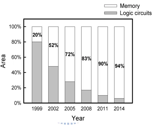
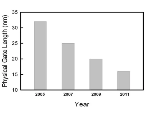
1.1 Semiconductor industry association (SIA) predicted the changes of area of embedded memory and logic circuits in a chip over year. The fraction of embedded memory continuously increasing from 20% and will reach 94% at year 2014. . . 3 1.2 The continuously scaling of physical gate length with years from ITRS
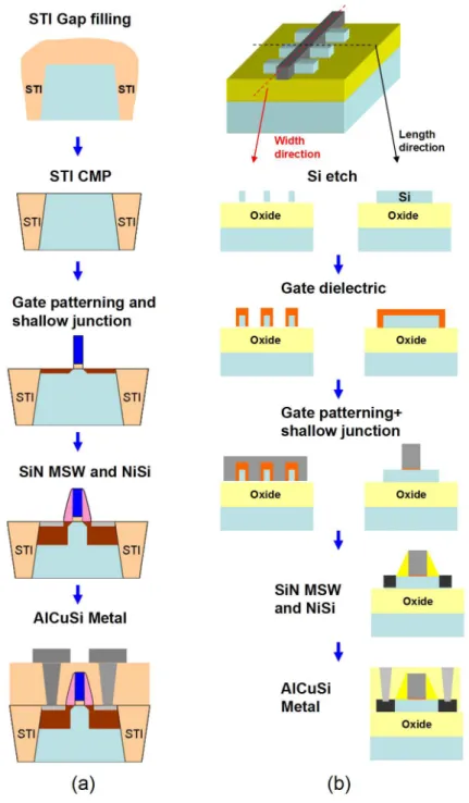
Roadmap 2005. The physical gate length is decreased from 32 nm to 16 nm during year 2005 to 2011. . . 4 2.1 Illustrations of (a) Planar MOSFET and (b) FinFET process flow in
Na-tional Nano Device Laboratories (NDL). The process flow has about 150 and 130 steps for Planar and FinFET devices, respectively. . . 14 2.2 Vth roll-off relation for estimation of σVth,P V E. The σVth,P V E can be
ex-tracted with the results of Vthroll-off and the gate length deviation and line
edge roughness induced σLg. . . 15
2.3 The scanning electron microscope image for multiple sampling, each sam-ple then mapped into the channel region to estimate the magnitude of the gate length deviation and the line edge roughness. . . 16 2.4 (a) Discrete dopants randomly distributed in the (80 nm)3 cube with the
average concentration of 1.48 × 1018 cm−3. There will be 758 dopants
within the cube, but dopants may vary from 0 to 14 ( the average number is 6 ) within its 125 sub cubes of 16 nm × 16 nm × 16 nm [(b and (c)]. . . 26 2.5 The histogram of the dopants in 125 sub cubes for 16 nm devices. The
dopants number can be describe by Gaussian Distribution with a mean of six. 27 2.6 The histogram of the dopants in 125 sub cubes for 65 nm devices. The
dopants number can be describe by Gaussian Distribution with a mean of 100. . . 28 2.7 The sub-cubes are equivalently mapped into channel region for discrete
dopant simulation as shown in MOSFET (a), and the same approach for SOI FinFET (b). The aspect ratio of FinFET is set at 2.0 rather than higher value to examine more critical situation. . . 29
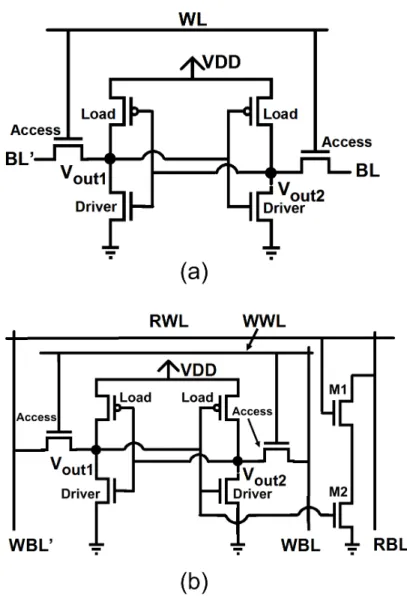
LIST OF FIGURES ix 2.8 The schematics of 6T (a) and 8T (b) SRAM cells. Since the bit-line voltage
will directly impact the “0” storage node in 6T structure during read oper-ation, additional transistors M1 and M2 in 8T structure is used to avoid the impact thus increase the read stability. . . 30 2.9 The flowchart for the mixed-mode device circuit coupling simulation. The
device’s simulation is performed first and get the initial solution of the de-vice’s potential. The mixed-mode simulation is then executed until the final step. . . 31 2.10 A flowchart of the decoupling algorithm. First we solve the nonlinear
Pois-son equation until it is convergence, and then the current continuity equa-tion of electron and hole is following solved. If the error is less than the tolerance, the program stops. . . 32 2.11 A flowchart for solving decoupled PDE. First the simulation domain have
to be discretized. Applying the finite element method approximation to the decoupled PDE, we obtained the nonlinear algebraic equations correspond-ing to the discretized grid. The Newton linearization method is then used to linearized the nonlinear equations. Finally, the linear algebraic equations can be solved using either direct or iterative method. . . 33
3.1 (a) DC characteristic fluctuations of ID − VG characteristics, the solid line
shows the nominal case and the dashed lines are random-dopant-fluctuated devices. (b) Vth fluctuated of 16-nm-gate planar MOSFET. The Vthis
de-fined as the gate voltage where the drain current is equal to 0.1 µA. Each symbol indicates one discrete dopant fluctuated case. The threshold volt-age may result from discrete-dopant-number and discrete-dopant-position induced fluctuations. . . 37 3.2 Extracted band profile for (a) nominal case and (b) discrete-dopant-fluctuated
case. Several potential barriers in the discrete-dopant fluctuated case are induced by the corresponding dopants in device’s channel and therefore change the threshold voltage. . . 38 3.3 Example of a 16 nm planar MOSFET with atomistic doping profiles both
in the channel and source/drain regions. (a) The actual locations of ran-dom discrete dopants and (b) the fluctuation in electrostatic potential are illustrated. . . 39
LIST OF FIGURES xi 3.4 Comparison of RDF effect in channel versus source/drain (S/D) region of
a planar MOSFET. The Vthfluctuations are 61 mV and 25 mV for channel
and S/D RDF only cases, respectively. The Vth fluctuation is 68 mV for
both channel and S/D RDF cases. Note that the channel RDF introduced around 90% of Vthfluctuation. . . 40
3.5 Vthfluctuation induced by (a) RDF and (b) PVE for different gate lengths
of n-type planar MOSFETs. As the gate length scaled from 65 to 16nm, the
Vthis decreased and both RDF and PVE induced fluctuations dramatically
increased as well. . . 42 3.6 (a)The static noise margin is defined as the minimum noise voltage present
at each of the cell storage nodes necessary to flip the state of the cell. (b)Graphically, this may be seen as moving the static characteristics ver-tically or horizontally along the side of the maximum nested square until the curves intersect at only one point [4]. . . 44 3.7 Nominal and fluctuated static transfer characteristics of 65 nm planar SRAM
cells. The solid line and the dashed lines stand for the nominal case and intrinsic parameter fluctuated cases, respectively, and the nominal SNM is 138 mV. . . 47
3.8 Static noise margin (SNM) fluctuations induced by (a) RDF and (b) PVE for different gate lengths of SRAM cells. The SNM significantly reduced from 138 mV to 20 mV, and the fluctuations increased as gate size scaled down. . . 48 3.9 Summary of normalized PVE and RDF induced SNM variation for 16 nm
to 65 nm planar SRAM. The RDF and PVE induced significantly normal-ized SNM fluctuations increased from 4.3% to 79.7%. and 2.1% to 31.1%, respectively. . . 49 3.10 The influence of different transistor pairs on total SNM fluctuation of planar
6T SRAM cell, where the Vthof devices are 350 mV. The access transistors
contribute most SNM fluctuation due to the stored date have to be read out through these two transistors. . . 52 4.1 Nominal and fluctuated static transfer characteristics of 8T SRAM cells,
where the SNM is increased to 233 mV, PVE and RDF induced SNM fluc-tuation are 14.9 mV and 22.1 mV, respectively. . . 56 4.2 Comparison of characteristic fluctuation for 8T SRAM and 6T SRAM with
cell ratio equal to two. The SNM and intrinsic-parameter-induced SNM fluctuation of 6T SRAM are about 84 mV and 20.0 mV, respectively. . . 57
LIST OF FIGURES xiii 4.3 The influence of different transistor pairs on total SNM fluctuation of
pla-nar 8T SRAM cell, where the Vth of devices are 140 mV. Compared with
6T SRAM, the impact of access transistors is significantly reduced due these two transistors are turned off during read operation, and the driver transistors become the dominating factor of the SNM fluctuation. . . 58 4.4 Nominal and fluctuated static transfer characteristics of improved 6T SRAM
cells, where the Vthof devices were raised to 350 mV. The SNM increased
to 92 mV, PVE and RDF induced fluctuation are 16.6 mV and 38.3 mV, respectively. . . 61 4.5 There will be 758 dopants are within a large rectangular solid, in which
the equivalent doping concentration is 1.48 × 1018 cm−3. The dopant
dis-tribution in the direction of channel depth, follows the normal disdis-tribution (b). The partitioned cubes are equivalently mapped into channel region for dopant position/number-sensitive device simulation (c). Similarly, dopants within the 16 nm3cubes may vary from zero to 14 (the average number is
six) (d). The vertical dopant distribution of the improved and the original doping profile, are shown in (e) and (f). . . 62
4.6 Nominal and fluctuated static transfer characteristics of 16 nm with higher
Vth devices and vertical doping profile engineering, where the SNM is 71
mV, PVE and RDF induced fluctuation are 17.3 mV and 21.7 mV, respec-tively. The reduced SNM and increased PVE induced fluctuation are result from enhanced short channel effect (SCE). . . 63 4.7 (a) Discrete dopants randomly distributed in the large cube with the average
concentration of 1.48 × 1018cm−3. There will be 1516 dopants within the
large cube, dopants may vary from 2 to 23 (average = 13) within sub cubes of 16 nm × 16 nm × 32 nm [(b) and (c)]. The sub-cubes are equivalently mapped into channel region of SOI FinFET for discrete dopant simulation as shown in (d). . . 67 4.8 Nominal and fluctuated static transfer characteristics of 16 nm SOI FinFET
SRAM cells, where the nominal SNM is 125 mV. . . 68 4.9 Summary of RDF and PVE induced normalized SNM fluctuation and
nom-inal SNM for different improvement techniques. For circuit level improve-ment, 8T SRAM reveals higher SNM and lower SNM fluctuation than 6T SRAM with CR = 2. For device level improvement, SOI FinFET SRAM increased the SNM to 125 mV and the normalized RDF and PVE induced SNM fluctuation are suppressed to 5.3% and 1.2%, respectively. . . 69
Chapter 1
Introduction
1.1 Motivation
As many consumer electronics products rapid developed, the function of the System-on-a-Chip (SoC) devices become more complex and the demand of embedded memory are increasing as well. Due to the better robustness, Static Random Access Memory (SRAM) are widely used as embedded cache memory in high performance integrated-circuits (ICs) and SoC applications. In fact, Semiconductor Industry Association (SIA) predicted that embedded SRAM arrays expected to occupy more than 90% of SoC area in next few years, as shown in Fig. 1.1. As a result, the increasing area of embedded SRAM makes it dominate the yield, stability and reliability of complementary metal-oxide-semiconductor (CMOS) computing chips.
Although large fast SRAM array has a great benefit to the system performance, the accompanied large area requirement directly impacts the costs of a chip. It is known that the most effective way to strike a balance is the process technology scaling. Figure 1.2 shows the physical gate length of metal-oxide-semiconductor field effect transistors (MOSFETs) roll-off follows the International Technology Roadmap for Semiconductors (ITRS). However, as the dimension of CMOS devices shrunk into sub-65 nm, double-digit channel dopants make transistor behaviors more complicated to be characterized with con-ventional “continuum modeling”. Random nature of discrete dopant distribution results in significantly random fluctuations, such as the deviation of threshold voltage (Vth), drive
current mismatch, and so on. The modern scaled-down devices and characteristics mis-matches make maintaining an acceptable Static Noise Margin (SNM) in SRAM becomes more challenging.
1.1 : Motivation 3
Figure 1.1: Semiconductor industry association (SIA) predicted the changes of area of embedded memory and logic circuits in a chip over year. The fraction of embedded memory
continuously increasing from 20% and will reach 94% at year 2014.
Figure 1.2: The continuously scaling of physical gate length with years from ITRS Roadmap 2005. The physical gate length is decreased from 32 nm to 16 nm during year 2005 to 2011.
1.2 : Literature Review 5
1.2 Literature Review
As the dimension of complementary metal-oxide-semiconductor (CMOS) devices shrunk into sub-65nm scale, the threshold voltage (Vth) fluctuation is pronounced and becomes
cru-cial for the design window, yield, noise margin, stability, and reliability of ultra large-scale integration circuits [1–5]. Various randomness effects resulted from the random nature of manufacturing process have induced significant fluctuations of electrical characteris-tics in nanometer scale (nanoscale) devices and circuits. The process-variation-induced gate length deviation and line edge roughness (PVE) are growing worse due to serious short-channel effect when the dimension of device is further scaled [6, 7]. Besides the pro-cess variation induced threshold voltage fluctuation (σVth,P V E), the double-digit channel
dopants in scaled channel size make transistor behaviors more complicated to be character-ized with conventional “continuum modeling” because every “discrete” dopant has its sig-nificant weight impacting the resulting transistor performance. The random nature of dis-crete dopant distribution results in significantly random fluctuations, such as the fluctuation of threshold voltage (σVth,RDF). The random dopant fluctuation (RDF) is unpredictable and
caused by random uncertainties in the fabrication process such as microscopic fluctuations in the number and location of dopant atoms in the channel region [5–11] and therefore is hard to be characterized. Diverse approaches have recently been presented to investigate fluctuation-related issues in semiconductor devices [12–19] and circuits [5, 12, 20, 22–25].
The intrinsic parameter fluctuations can limit the performance, yield and functionality due to significant component mismatch in area constrained circuits, such as static random ac-cess memory (SRAM). A SRAM cell can operated in three different states: standby, write, and read. Due to the cell is most vulnerable to noise during read operation [3,4], the stabil-ity of a SRAM cell is often related to the static noise margin (SNM). The SNM is defined as the maximum DC noise voltage tolerance to avoid the cell state been flipped during a read access. Several studies have been made on investigating the effect of random dopant fluctuation in SRAM circuits by compact modeling approach [1–4, 26, 27]. However, such approach cannot take the random-dopant-position-induced fluctuation into consideration, which may lead to 50% error in threshold voltage fluctuation [28].
1.3 : The Study of this Thesis 7
1.3 The Study of this Thesis
In this thesis, an experimental validated three-dimensional “atomistic” coupled device-circuit simulation approach is thus employed to analyze the process-variation and random dopant induced characteristic fluctuations in nanoscale SRAM circuit. Not only conven-tional 6T SRAM but also the 8-Transistors structure [29] had been investigated, which is proposed to increase the SNM. The statistically generated large-scale doping profiles are similar to the physical process of ion implantation and thermal annealing [30]. Based on the statistically generated large-scale doping profiles, device simulation is performed by solving a set of three-dimensional (3D) drift-diffusion equations with quantum cor-rections by the density gradient method, which is conducted using a parallel computing system [31–33]. In estimation of the characteristics variations in circuit, for obtaining more physical insight device and pursuing higher accuracy [34], a coupled device-circuit simulation [35–37] with discrete dopant distribution is conducted to examine the associated behavior of circuit, which concurrently considers the dopant-number- and discrete-dopant-position-induced fluctuations. We notice that the accuracy of developed analyzing technique has been quantitatively verified in the experimentally measured characteristics of sub-20 nm devices [6–9, 38]. The function-dependent and circuit-topology- dependent characteristic fluctuations resulted from random nature of discrete dopants is for the first time discussed.
1.4 Outline
The thesis is organized as follows. In Chap. 2, we introduce the analyzing technique for studying the random dopants effect in nanoscale device and circuit. In Chap. 3, we examine the discrete-dopant- and process-variation-induced characteristic fluctuations of the investigated device and SRAM circuit. In Chap. 4, Both device and circuit level char-acteristic fluctuations suppression approaches are discussed. Finally, we draw conclusions and suggestion future work in Chap. 5.
Chapter 2
Fabrication and Simulation
I
n this chapter, a large-scale statistically sound “atomistic” device-circuit coupled sim-ulation approach is proposed to characterize the random-dopant-induced characteristic fluctuations when the gate length of CMOS integrated circuits is down to 16 nm concur-rently capturing the discrete-dopant-number- and discrete-dopant-position-induced fluctu-ations. We experimentally quantified the random dopant fluctuation (RDF) induced thresh-old voltage (Vth) standard deviation up to 40 mV for sub-20-nm-gate planar complementarymetal-oxide-semiconductor (CMOS) field effect transistors. The accuracy of the simulation technique is confirmed by the use of experimentally calibrated transistor physical model.
2.1 Manufacturing Process
The standard CMOS process flow in National Nano Device Laboratories (NDL) is sum-marized as following:
1. Active area patterning
2. Shallow trench isolation (STI) formation (chemical-mechanical polishing (CMP)) 3. Narrow width device trimmed down upon STI etching
4. P/N-well implant
5. Gate oxide and poly gate patterning (I-line ready, deep-UV under planning) 6. Re-oxidation
7. N/P halo and lightly doped drain shallow junction 8. SiN MSW
9. N+/P+source/drain
10. Spike rapid thermal anneal (RTA) 11. Low-temperature annealing NiSi
12. Strained SiN contact etch stop layer (CESL) and interlayer dielectric (ILD) 13. Contact patterning (I-line ready, deep-UV under planning)
14. Ti/TiN/AlCuSi/TiN deposition 15. M1 patterning
16. Interlayer dielectric deposition and chemical-mechanical polishing (CMP) 17. Via patterning
18. Ti/TiN/AlCuSi/TiN deposition 19. Sintering
2.1 : Manufacturing Process 11 The entire process flow for planar MOSFET contains about 150 steps, which may take 3 to 4 months. Manufacturing process of FinFET devices is highly similar with the planar devices except step 2 to 4, which will reduce around 20 process steps in total. Figs. 2.1(a) and 2.1(b) illustrate several key process steps for planar MOSFET and FinFET, respec-tively. The process is started from active area patterning. After shallow-trench isolation (STI) formation, the device width is trimmed down upon STI etching. Channel doping is performed to adjust threshold voltage (Vth) of transistor, using masked ion implantation.
To relieve the etch damage, a sacrificial oxide is removed before gate oxidation. Thermal oxide is grown and in-situ heavily doped N+poly-silicon is deposited. After the deposition
and trimmed down of gate hard mask, the pocket implantation technique is used for the suppression of the short channel effect. Composite spacer of silicon oxide and nitride is deposited and etched anisotropically. After the gate and spacer formation, heavily doped N+junction are made with Phosphorous implantation. Low-thermalbudget activation
pro-cess is used for dopant activation and control of doping profile. After inter-layer-dielectric deposition, wolfram is used for metal contact plugging and copper is used for interconnec-tion. Finally, alloying anneal is performed. We notice that the narrow width device trimmed down upon STI etching and low-thermal-budget activation process are the critical steps in fabrication of sub-20 nm transistor. Threshold voltage (Vth) is one of the key device
(MOSFETs). As the mean gate length deviation (GLD), the line edge roughness (LER), and random doping (RD) are the major variation sources of threshold voltage, we can thus extract the random doping induced standard Vth deviation, σVth,RDF, from the following
approximated equation
(σVth,T otal)2 ≈ (σVth,RDF)2+ (σVth,P V E)2, (2.1)
where σVth,T otalis the standard deviation of total Vth, σVth,RDF is RDF induced threshold
voltage fluctuations, and σVth,P V E is PVE induced threshold voltage fluctuations which
contributed from the gate length deviation and the line edge roughness. The σVth,T otalcan
be directly measured from the experimental data. For the σVth,P V E, by using the Vthroll-off
relation
σVth,P V E = dVt
dLg
× σLg, (2.2)
where the σVth,P V E can be extracted with the results of Vth roll-off and the gate length
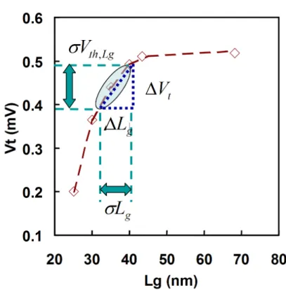
deviation and line edge roughness induced σLg, as shown in Fig. 2.2. The magnitude of
gate length deviation and line edge roughness are extracted from scanning electron micro-scope critical dimension measurements, as shown in Fig. 2.3. The resolution of σLg is 0.5
nm. Thus, from the experimentally measured σVth,T otal and extracted σVth,P V E, we can
calculate σVth,RDF according to Eq. (2.1).
The Eq. (2.1) implies two important insights:
2.1 : Manufacturing Process 13 2. σVth,T otalreduction more relies on dominant factor improving.
For example, by assuming the σVth,T otalof 50 mV and σVth,P V E of 25 mV, we can obtain
the σVth,RDF of 43 mV. If a new fluctuation source of 10 mV is introduced, the σVth,RDF
is still about 42 mV. The σVth,RDF is not be significantly influenced by the second order
factors. Since the σVth,T otalis dominated by σVth,RDF, the 15% reduction of σVth,RDF may
reduce the σVth,T otalby 12%. However, the 15% reduction of σVth,P V Ecan only reduce the
σVth,T otal by 4%. The result shows that the σVth,T otal reduction more relies on dominant
Figure 2.1: Illustrations of (a) Planar MOSFET and (b) FinFET process flow in National Nano Device Laboratories (NDL). The process flow has about 150 and 130 steps for Planar and FinFET devices, respectively.
2.1 : Manufacturing Process 15
Figure 2.2: Vthroll-off relation for estimation of σVth,P V E. The
σVth,P V Ecan be extracted with the results of Vthroll-off
and the gate length deviation and line edge roughness induced σLg.
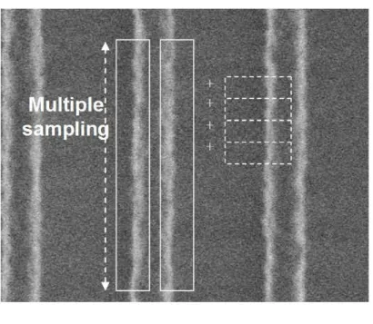
Figure 2.3: The scanning electron microscope image for multiple sampling, each sample then mapped into the channel region to estimate the magnitude of the gate length deviation and the line edge roughness.
2.2 : Simulation Technique 17
2.2 Simulation Technique
In this section, a large-scale statistically sound “atomistic” simulation approach is pro-posed to characterize the random-dopant-induced characteristic fluctuations in 16-nm-gate concurrently capturing the discrete-dopant-number- and discrete-dopant-position-induced fluctuations.
2.2.1 Physical Modelling and Numerical Methods
The technology computer-aided design (TCAD) simulations, such as process and de-vice simulations, are widely used for the analysis of semiconductor dede-vices. The process simulation can generate the device geometry and doping profile according to the parame-ters of the fabrication processes. The output of process simulation is then used in the device simulation to estimate device characteristics. The drift-diffusion (DD) and hydrodynamic (HD) models play a crucial role in the development of semiconductor device simulator in the macroscopic point of view. The DD model was derived from Maxwell’s equation as well as charges’ conservation law and has been successfully applied to study device trans-port behavior, in the past decades. It assumes local isothermal conditions and is still widely employed in semiconductor device design.
Classical drift-diffusion model consists of at least three coupled partial differential equations (PDEs) for, such as electrostatic potential and electron-hole densities. When
device channel is specified, a set of the DD equations in semiconductor device simulation is solved: 4φ = q εs (n − p + D), (2.3) 1 q 5 ·Jn = R(n, p), (2.4) and 1 q 5 ·Jp = −R(n, p), (2.5)
where φ is the electrostatic potential and its unit is volt. n and p are classical electron and hole concentrations (cm−3). q is the elementary charge and its unit is coulomb. The net
doping concentration is D(x, y, z) = N+
D(x, y, z)−NA−(x, y, z). R is the net recombination
rate (cm−3s−1). The carrier’s currents densities are given by
Jn = −qµnn 5 φ + qDn5 n + unkBn 5 Tn, (2.6)
and
Jp = −qµpp 5 φ + qDp5 p + upkBp 5 Tp, (2.7)
where µnand µpare the carrier mobility (cm2/V − s). The diffusion coefficients, Dnand
2.2 : Simulation Technique 19 The mobility model used in the device simulation, according to Mathiessen’s rule [39– 41], can be empirically expressed as:
1 µ = G µsurf aps + G µsurf rs + 1 µbulk , (2.8) where G = exp(x/lcrit), x is the distance from the interface and lcrit is a fitting parameter.
The mobility consists of three parts: (1) the surface contribution due to acoustic phonon scattering µsurf aps = B E + C(Ni/N0)τ E13(T /T0)K , (2.9) where Ni = NA+ ND, T0 = 300K, E is the transverse electric field normal to the
inter-face of semiconductor and insulator, B and C are parameters which based on physically derived quantities, N0 and τ are fitting parameters, T is lattice temperature, and K is the
temperature dependence of the probability of surface phonon scattering; (2) the contribu-tion attributed to surface roughness scattering is
µsurf rs = ( (E/Eref)Ξ δ + E3 η ) −1, (2.10) where Ξ = A + α(n+p)Nrefυ
(Ni+N1)υ , Eref = 1 V /cm is a reference electric field to ensure a unitless
numerator in µsurf rs, Nref = 1 cm−3is a reference doping concentration to cancel the unit
of the term raised to the power υ in the denominator of Ξ, δ is a constant that depends on the details of the technology, such as oxide growth conditions, N1 = 1 cm−3, A, α and η
are fitting parameters; (3) and the bulk mobility is
µbulk = µL(
T−ξ
T0
), (2.11) where µLis the mobility due to bulk phonon scattering and ξ is a fitting parameter.
The quantum mechanical effects should be considered in the device simulation when the dimensions of the devices shrunk into nanometer scale. Various theoretical approaches have been presented to study the quantum confinement effects, such as full quantum me-chanical model (e.g. nonequilibrium Green’s function) and quantum corrections to the clas-sical drift-diffusion (DD) or hydrodynamic (HD) transport models. A set of Schr¨odinger-Poisson (SP) equations has been applied to study the quantum effect in the inversion layers, but it is a time-consuming task in the TCAD application to realistic device characterization. Therefore, various quantum correction models, H¨ansch, modified local density approxima-tion (MLDA), effective potential (EP), density gradient (DG) and so on, have been pro-posed for classical DD or HD transport models. In this investigation, the density gradient was coupled with the DD model and solved for the quantum mechanical effects. The den-sity gradient equation can be expressed as,
~
Jn= −qµnn 5 φ + qDn5 n − qnµ 5 (2bn
52√n
√
n ), (2.12)
where bn = ~2/(12qm∗n) and m∗n = mk× 9.11 × 10⁻³¹kg. bn in Eq. (2.12) is the density
2.2 : Simulation Technique 21 The last term in the right hand side of Eq. (2.12) is referred to as “quantum diffusion”, which makes the electron continuity equation has a fourth-order partial differential equa-tion. Therefore, such an approach is highly sensitive to noise in the local carrier density, and the methodology is highly important in cases of strong quantization. To calculate the numerical solution of the multidimensional density-gradient model, firstly we decouple the coupled partial differential equations (PDEs); approximated with the finite volume method over nonuniform mesh. The corresponding system of the nonlinear algebraic equations is then solved with the mixed monotone iteration and Newton’s iteration methods. Iteration will be terminated and postprocesses will be performed when the specified stopping criteria for inner and outer iteration loops are satisfied, respectively.
The nominal channel doping concentrations are 1.48 × 1018cm−3 and the V
th are
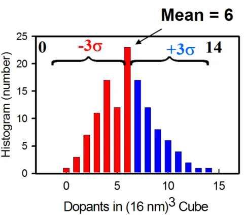
cal-ibrated for 16-nm-gate MOSFETs. For RDF, to consider the random fluctuation effect of the number and location of discrete channel dopants, 758 dopants are randomly generated in a large cube (80 nm × 80 nm × 80 nm), in which the equivalent doping concentration is 1.48 × 1018 cm−3, as shown in Fig. 2.4(a). To determine the location of each dopant,
first we use Mersenne Twister algorithm [42] to generate double-precision values in the closed interval [2−53, 1 − 2−53]. Then multiplied the generated values by the side length
of the large cube, we obtain x-, y-, and z-coordinate value of the dopant. The large cube is then partitioned into 125 sub-cubes of (16 nm × 16 nm × 16 nm). The number of
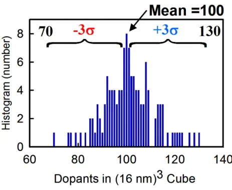
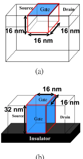
dopants may vary from zero to 14, and the average number is 6, as shown in Figs. 2.4(b) and 2.4(c), respectively. In principle, 3D device simulation with the 125 channel structures almost covers cases, shown in Fig. 2.5, and thus will be fairly meaningful to reflect statis-tical randomness of dopant number. We have noticed that in this simulation only dopant within the channel region is treated discretely.The doping concentrations remain contin-uous in the source/drain region because the volume of source/drain region is two-order magnitude greater than that of channel region. Similarly, we can obtain the distribution of dopant number for the 65-nm-gate transistor, in which the dopant number may vary from 70 to 130 as shown in Fig. 2.6. These sub-cubes are equivalently mapped into the de-vice channel for the 3D “atomistic” dede-vice simulation with discrete dopants, as shown in Fig. 2.7(a). In “atomistic” device simulation, the resolution of individual charges within a conventional drift-diffusion simulation using a fine mesh creates problems associated with singularities in the Coulomb potential [43–45]. The potential becomes too steep with fine mesh, and therefore, the majority carriers are unphysically trapped by ionized impurities, and the mobile carrier density is reduced [43–45]. Thus, the density-gradient approxima-tion is used to handle discrete charges by properly introducing related quantum-mechanical effects, and coupled with Poisson equation as well as electron-hole current continuity equa-tions [46–54]. Fig. 2.7(b) shows the studied SOI FinFET with aspect ratio (defined by the fin height / the fin width) equal to two. Without losing generality, the SOI FinFET is with
2.2 : Simulation Technique 23 16-nm-gate and 1.48 × 1018cm−3 equivalent channel doping concentration. The explored
6T and 8T SRAM circuits are illustrated in Fig. 2.8(a) and 2.8(b), respectively. As the di-mension of devices continuously scaling, the 8-transistors structure is proposed to increase the static noise margin. Unlike the 6T SRAM, the access transistors are turned off during the read operation in the 8T cell, the stored data is read out through additional transistors M1 and M2 passively, which avoid the bit line impact the data directly. Thus increase the SNM. All cell ratios (CR; CR = (W/L)driver transistor
(W/L)access transistor) of the SRAM cells in this thesis are
first set at unitary. The applied voltages of 16 nm and 65 nm devices are 1.0 and 1.2 volt, re-spectively. The physical model and accuracy of such large-scale simulation approach have been quantitatively calibrated by experimentally measured results [5–9]. Similarly, we can generate 125 discrete-dopant-fluctuated cases for PMOSFET through the flow of Figs. 2.4-2.6. Then, 125 pairs of NMOSFETs and PMOSFETs are randomly selected and are used for the examination of circuit characteristics fluctuations. Furthermore, we apply the sta-tistical approach to evaluate the effect of PVE, in which the magnitude of the gate length deviation and the line edge roughness follows the projections of the ITRS 2007 [55]. The 3σ for process variation induced gate length deviation and line edge roughness are 1.5 nm and 4.3 nm for the 16 nm and 65 nm devices, respectively. In estimating circuit characteris-tics, ultra-small nanoscale devices, and for capturing the discrete-dopant-position-induced
fluctuations, a device-circuit coupled simulation approach [5] is employed. The nodal volt-age and loop current in the circuit can be calculated. The formulation of circuit equations is mainly base upon the Kirchhoff’s current law. The circuit nodal equation of 6T SRAM, as illustrated in Fig. 2.8(a), is shown in below:
Node1 : V1 = VDD, (2.13)
Node2 : V2 = VBL, (2.14)
Node3 : V3 = VBL0, (2.15)
Node4 : V4 = 0, (2.16)
Node5 : V5 = VW L, (2.17)
Node6 : Id,P M OS2+ Id,N M OS4= Id,N M OS2, (2.18)
and
Node7 : Id,P M OS1+ Id,N M OS3= Id,N M OS1, (2.19)
The static transfer characteristics of SRAMs are then estimated. Thus, all device and circuit characteristics are obtained without any devices’ equivalent circuit models. The flowchart
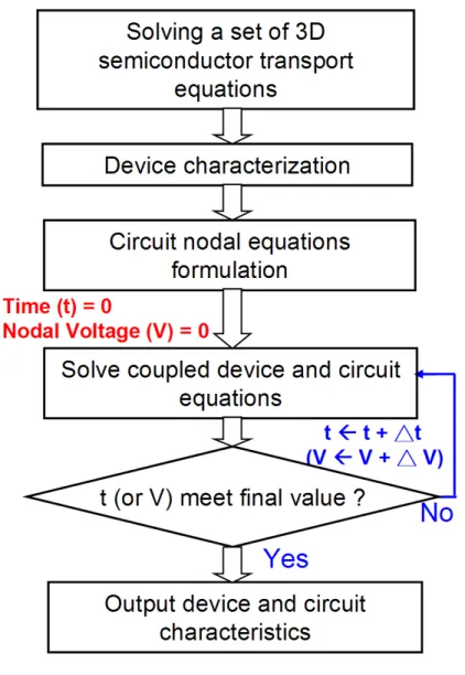
2.2 : Simulation Technique 25 for mix-mode simulation method is shown in Fig. 2.9. The characteristics of devices of test circuit are first estimated by solving the device transport equations and using as initial guesses in the device-circuit coupled simulation. The circuit nodal equations of the test circuit are formulated and then directly coupled to the device transport equations (in the form of a large matrix containing the circuit and device equations), which are solved si-multaneously to obtain the circuit characteristics [5]. The flowchart of decoupled PDE is shown in Fig. 2.10. First we solve the nonlinear Poisson equation until it is convergence, and then the current continuity equation of electron and hole is following solved. If the error is less than the tolerance, the program stops and output the initial solution of device’s potential and perform the mixed-mode simulation. We solve the device’s equations cou-pled with circuit nodal equations until it is convergence. Figure 2.11 shows the flow for solving decoupled PDE. First the simulation domain have to be discretized. Applying the finite element approximation to the decoupled PDE, we obtained the nonlinear algebraic equations corresponding to the discretized grid. The Newton linearization method is then used to linearized the nonlinear equations. Finally, the linear algebraic equations can be solved using either direct or iterative method.
Figure 2.4: (a) Discrete dopants randomly distributed in the (80 nm)3
cube with the average concentration of 1.48 × 1018cm−3.
There will be 758 dopants within the cube, but dopants may vary from 0 to 14 ( the average number is 6 ) within its 125 sub cubes of 16 nm × 16 nm × 16 nm [(b and (c)].
2.2 : Simulation Technique 27
Figure 2.5: The histogram of the dopants in 125 sub cubes for 16 nm devices. The dopants number can be describe by Gaussian Distribution with a mean of six.
Figure 2.6: The histogram of the dopants in 125 sub cubes for 65 nm devices. The dopants number can be describe by Gaussian Distribution with a mean of 100.
2.2 : Simulation Technique 29
Figure 2.7: The sub-cubes are equivalently mapped into channel region for discrete dopant simulation as shown in MOSFET (a), and the same approach for SOI FinFET (b). The aspect ratio of FinFET is set at 2.0 rather than higher value to examine more critical situation.
Figure 2.8: The schematics of 6T (a) and 8T (b) SRAM cells. Since the bit-line voltage will directly impact the “0” storage node in 6T structure during read operation, additional transistors M1 and M2 in 8T structure is used to avoid the impact thus increase the read stability.
2.2 : Simulation Technique 31
Figure 2.9: The flowchart for the mixed-mode device circuit coupling simulation. The device’s simulation is performed first and get the initial solution of the device’s potential. The
Figure 2.10: A flowchart of the decoupling algorithm. First we solve the nonlinear Poisson equation until it is convergence, and then the current continuity equation of electron and hole is following solved. If the error is less than the tolerance, the program stops.
2.2 : Simulation Technique 33
Figure 2.11: A flowchart for solving decoupled PDE. First the simulation domain have to be discretized. Applying the finite element method approximation to the decoupled PDE, we obtained the nonlinear algebraic equations corresponding to the discretized grid. The Newton linearization method is then used to linearized the
nonlinear equations. Finally, the linear algebraic equations can be solved using either direct or iterative method.
Intrinsic Parameter Fluctuation on
Devices and SRAM Cells
I
n this chapter, the device intrinsic parameter induced characteristics fluctuations on 65-nm to 16-65-nm-gate planar devices were first explored. Then we introduce the stability of an SRAM cell. Finally, the device intrinsic parameter induced SNM fluctuations on 65-nm to 16-nm-gate planar 6T SRAM cells and the correlation between total SNM fluctuation and different transistor pairs were examined.3.1 : Physical Characteristics 35
3.1 Physical Characteristics
Figure 3.1(a) shows the ID − VG characteristics fluctuations of the
discrete-dopant-fluctuated 16 nm planar MOSFETs, where the solid line shows the nominal case (contin-uously doped channel with 1.48 × 1018 cm−3 doping concentration) and the dashed lines
are random-dopant-fluctuated devices. From the random-dopant-number point of view, the equivalent channel doping concentration is increased when the dopant number increases, which substantially alters the threshold voltage as shown in Fig. 3.1(b). The threshold voltage is determined from a current criterion that the drain current larger than 10−7(W/L)
ampere. As the number of dopants in channel is increased, the device’s Vth is increased.
The position of random dopants induced different fluctuation of characteristics in spite of the same number of dopants. For the device with the number of discrete dopants, varying from zero to 14, maximum difference of Vth is about 240 mV, which takes an important
part in random dopant fluctuation. Furthermore, the magnitude of the spread characteris-tics increases as the number of dopants increases. The physical mechanism can be briefly described by band profile. Figures 3.2(a) and 3.2(b) show the extracted band profile for the nominal case and discrete-dopant-fluctuated case, respectively. For the nominal case, the band profile is smooth. However, there are several potential barriers in the discrete-dopant fluctuated case. These potential barriers are induced by the corresponding discrete-dopants in device’s channel and therefore change the threshold voltage.
Both the randomness of dopants in the channel and source/drain regions may induce the Vth fluctuation in a planar MOSFET device. In order to verify the importance of the
RDF in the channel region, the RDF in source and drain regions is also investigated. An example of a 16-nm-gate planar MOSFET with atomistic doping profiles both in the chan-nel and source/drain regions is shown in Fig. 3.3. The actual location of random discrete dopants and the electrostatic potential are illustrated in Fig. 3.3(a). Note that the atom-istic doping in the source/drain of device will not only introduce the electrostatic potential fluctuation but also the variations in the effective length of the channel as shown in Fig. 3.3(b). Fig. 3.4 shows the comparison of RDF effect in channel versus source/drain region. The Vth fluctuations are 61 mV and 25 mV in channel and source/drain RDF only cases,
respectively. Moreover, the fluctuation is only 68 mV for both channel and source/drain RDF cases. It can be seen that the influence of channel RDF on Vth fluctuation is around
90%, which means the Vthfluctuation in a planar MOSFET is dominated by the
random-ness of dopants in the channel rather than the source/drain region. Therefore, RDF in the source/drain region can be neglected and won’t be considered in following study.
3.1 : Physical Characteristics 37
Figure 3.1: (a) DC characteristic fluctuations of ID− VGcharacteristics,
the solid line shows the nominal case and the dashed lines are random-dopant-fluctuated devices. (b) Vthfluctuated of
16-nm-gate planar MOSFET. The Vthis defined as the gate
voltage where the drain current is equal to 0.1 µA. Each symbol indicates one discrete dopant fluctuated case. The threshold voltage may result from discrete-dopant-number and discrete-dopant-position induced fluctuations.
Figure 3.2: Extracted band profile for (a) nominal case and (b)
discrete-dopant-fluctuated case. Several potential barriers in the discrete-dopant fluctuated case are induced by the corresponding dopants in device’s channel and therefore change the threshold voltage.
3.1 : Physical Characteristics 39
Figure 3.3: Example of a 16 nm planar MOSFET with atomistic doping profiles both in the channel and source/drain regions. (a) The actual locations of random discrete dopants and (b) the fluctuation in electrostatic potential are illustrated.
Figure 3.4: Comparison of RDF effect in channel versus source/drain (S/D) region of a planar MOSFET. The Vthfluctuations are
61 mV and 25 mV for channel and S/D RDF only cases, respectively. The Vthfluctuation is 68 mV for both channel
and S/D RDF cases. Note that the channel RDF introduced around 90% of Vthfluctuation.
3.2 : Intrinsic Parameter Fluctuation on Devices 41
3.2 Intrinsic Parameter Fluctuation on Devices
Figure 3.5(a) and Fig. 3.5(b) show the RDF and PVE induced threshold voltage (Vth)
fluctuations for the 16 nm to 65 nm gate n-type planar MOSFETs, respectively. The nomi-nal value of threshold voltage is rolled-off as the gate length decreased, where the nominomi-nal
Vthfor 16, 32, and 65 nm devices are 140, 220, and 280 mV. Based upon the independency
of the fluctuation components, the total Vthfluctuation (σVth,T otal) is given by Eq. (2.1). As
the gate length scales from 65 nm to 16 nm, the Vthfluctuation increases significantly from
16 mV to 64 mV. The RDF induces 15.8 mV, 30 mV and 61 mV Vthfluctuations are in 65
nm, 32 nm and 16 nm devices, respectively. The Vth fluctuation of 16 nm MOSFET is 4
times larger than that of 65 nm, which follows the trend of analytical shown in below [11].
σVth,RDF = 3.19 × 10⁻⁸
tox√NA0.401
W L , (3.1)
where the tox is the thickness of gate oxide; W and L are the width and length of the
transistor. Therefore, the simulation accuracy for device characteristics fluctuation is con-firmed. Additionally, as shown in Fig. 3.5, the RDF dominates the total Vth fluctuation in
the explored device dimensions. The RDF induces 5 and 3.5 times larger Vth fluctuation
than PVE for 65-nm and 16-nm-gate device, respectively. The increasing fluctuations of such extreme small components may cause critical issue of stability.
Figure 3.5: Vthfluctuation induced by (a) RDF and (b) PVE for
different gate lengths of n-type planar MOSFETs. As the gate length scaled from 65 to 16nm, the Vthis decreased
and both RDF and PVE induced fluctuations dramatically increased as well.
3.3 : SRAM Stability 43
3.3 SRAM Stability
The stability of SRAM cell is often related to the static noise margin, due to the cell is most vulnerable to noise during a read access since the “0” storage node rises to a volt-age higher than ground due to a voltvolt-age division along the access and inverter pull-down NMOSFET devices between the precharged bitline (BL) and the ground terminal of the cell [4]. There are several definitions of the static noise margin, one of the common used approach of estimating SNM is first proposed by Hill [56] and been used in this thesis. In this approach, an SRAM cell is seen as two equivalent inverters with the noise sources insert between the corresponding inputs and outputs as shown in Fig. 3.6(a). Both series voltage noise sources (Vn) have the same value and act together to upset the state of the
cell. Applying the adverse noise sources polarity represents the worst-case equal noise margins [57]. This method is only applicable to circuits with Rin À Rout, and CMOS
in-verters of an SRAM cell comply with this condition [58]. Graphically, this may be seen as moving the static characteristics vertically or horizontally along the side of the maximum nested square until the curves intersect at only one point as shown in Fig. 3.6(b) [4].
Figure 3.6: (a)The static noise margin is defined as the minimum noise voltage present at each of the cell storage nodes necessary to flip the state of the cell. (b)Graphically, this may be seen as moving the static characteristics vertically or
horizontally along the side of the maximum nested square until the curves intersect at only one point [4].
3.4 : Intrinsic Parameter Fluctuation on SRAM Cells 45
3.4 Intrinsic Parameter Fluctuation on SRAM Cells
Figure 3.7 shows the static transfer characteristics of 65 nm planar SRAM cells in-cluding process variation and random dopant fluctuation, where the dashed lines represent intrinsic-parameter-fluctuated cases, and the solid line stands for the nominal case. The nominal SNM for the 65 nm planar MOSFET SRAM is 138 mV. Since the RDF induces larger device variability in threshold voltage, the SNM fluctuation of SRAM is thus dom-inated by RDF. The RDF- and PVE-induced SNM fluctuations are then summarized in Table 3.1, where the static noise margin deviation induced by PVE and RDF are 2.9 mV and 5.9 mV, respectively.
Figure 3.8 shows the roll-off characteristics of SNM for SRAM cells with different device gate length. The error bars in Figs. 3.8(a) and 3.8(b) represent the RDF- and PVE-induced SNM fluctuation, respectively. As gate length scales from 65 nm to 16 nm, the SNM decreases significantly from 138 mV to 20 mV. Moreover, the RDF is the most crit-ical issue in improving stability of SRAM. Figure 3.9 summarized the normalized SNM fluctuations for 65-, 32- and 16-nm-gate SRAM, where the normalized SNM fluctuation is defined as following:
Normalized σSNM = σSNM SNMnominal
, (3.2) where the σSNM is the SNM fluctuation and the SNMnominal is the nominal value of
gate length of device scaling from 65 nm to 16 nm, the RDF-induced normalized SNM fluctuation increases from 4.3% to 80%. The significant increase of SNM fluctuation re-veals the highly dependence of SNM fluctuation on the dimensions of transistors. Although the shrinking of the device size can increase the density of memory, the decreased SNM and increased SNM fluctuation are crucial issues and may limit the usage of such small device.
3.4 : Intrinsic Parameter Fluctuation on SRAM Cells 47
Figure 3.7: Nominal and fluctuated static transfer characteristics of 65 nm planar SRAM cells. The solid line and the dashed lines stand for the nominal case and intrinsic parameter fluctuated cases, respectively, and the nominal SNM is 138 mV.
Table 3.1: PVE and RDF induced SNM fluctuation in 65 nm planar SRAM, where the RDF dominates the SNM fluctuation
Fluctuation Source SNM Fluctuation PVE 2.9 mV RDF 5.9 mV
Figure 3.8: Static noise margin (SNM) fluctuations induced by (a) RDF and (b) PVE for different gate lengths of SRAM cells. The SNM significantly reduced from 138 mV to 20 mV, and the fluctuations increased as gate size scaled down.
3.4 : Intrinsic Parameter Fluctuation on SRAM Cells 49
Figure 3.9: Summary of normalized PVE and RDF induced SNM variation for 16 nm to 65 nm planar SRAM. The RDF and PVE induced significantly normalized SNM fluctuations increased from 4.3% to 79.7%. and 2.1% to 31.1%, respectively.
To confirm the simulation accuracy for circuit characteristic fluctuations and find out the most sensitive components in SRAM, the transistors in a 6T SRAM cell are classified into driver, access, and load transistors as shown in Fig. 2.8(a). Because the SNM of 6T SRAM for device with 140 mV Vthand unitary cell ratio is merely 20 mV, we adjusted the
Vthto 350 mV for more accurate sensitivity analysis. The SNM is thus increased to 92 mV
and the SNM fluctuation is 38 mV. We then analyzed the sensitivity of 16-nm-gate planar SRAM by investigating the random-dopant-effect in different transistor pair induced SNM fluctuation in Fig. 3.10. While investigating the SNM fluctuations induced by specific transistor pair, the investigated transistors are random-dopant-fluctuated and the others are nominal. The access transistors contribute the largest SNM fluctuations, which is 3 and 9 times higher than the other two transistor pairs because the stored data was read out through the access transistors during the read operation. Since the fluctuation distribution of each transistor pair in a SRAM cell is stochastic, the influences on total SNM fluctuation (σSNMT otal) can be seen as independent. Similar to the σVth, the relationship between
σSNMT otaland its components can be expressed as following:
(σSNMT otal)2 = (σSNMDriver)2+ (σSNMAccess)2+ (σSNMLoad)2, (3.3)
where the σSNMT otalis the total SNM fluctuation; σSNMDriver, σSNMAccess, and σSNMLoad
are the SNM fluctuation induced by driver, access, and load transistors. The σSNMT otal
3.4 : Intrinsic Parameter Fluctuation on SRAM Cells 51 shows a good agreement to the result obtaining from all transistor with fluctuation, 38 mV. The simulation accuracy for circuit characteristic fluctuations is therefore confirmed.
Since the SNM of 6T SRAM for device with 140 mV Vthand unitary cell ratio is 20 mV
with 80% normalized SNM fluctuation, which may not ensure correct operation of circuits, improvement and suppression approaches based on the circuit and device viewpoints are implemented to examine the associated characteristics in 16-nm-gate SRAM cells.
Figure 3.10: The influence of different transistor pairs on total SNM fluctuation of planar 6T SRAM cell, where the Vthof
devices are 350 mV. The access transistors contribute most SNM fluctuation due to the stored date have to be read out through these two transistors.
Chapter 4
Fluctuation Suppression Approaches
I
n this chapter, the fluctuation suppression approaches based on circuits and device viewpoints are presented.4.1 Circuit Level Improvement
From the circuit viewpoint, an 8T planar SRAM architecture as shown in Fig. 2.8(b) is first explored. Besides conventional 6T structure, the 8T SRAM cell is one kind of improved SRAM structures. The main purpose of 8T SRAM is to eliminate the impact of bit line to stored data during read operation by separating the data retention and data output elements. Unlike the 6T structure, the access transistors of 8T SRAM are turned off when data reading and the data will be gathered through the additional two transistors. This
mechanism can avoid direct flow between the bit line and the stored data and then increase the noise margin. Fig. 4.1 shows the static transfer characteristics of 8T SRAM cells including RDF-fluctuated cases, where the device Vthis 140 mV. Due to the separation of
data access element, the influence result from bit-line is reduced and increased the nominal SNM to 233 mV. The RDF induced SNM fluctuation is 22 mV, which is less than 10% variation. Comparing with original planar 6T SRAM cell, the nominal SNM is 12 times larger and normalized RDF induced SNM fluctuation is suppressed by a factor of 8.4. Notably, thought the 8T SRAM can enlarge the SNM and reduced the SNM fluctuation, the chip area is increased by 30% under our setting (all sizes of devices are the same), which may reduce the chip density. Figure 4.2 compares the SNM and SNM fluctuation for 8T SRAM and 6T SRAM with CR = 2. Similar to 8T SRAM, the 6T SRAM with CR = 2 also requires 30% extra chip area. The SNM and intrinsic-parameter-induced SNM fluctuation of 6T SRAM are about 84 and 20.0 mV, respectively. The extra requirement of chip area didn’t bring significant improvement as that of 8T SRAM. The sensitivity of SNM fluctuation induced by different transistors pair of planar 8T SRAM cell is analyzed, as shown in Fig. 4.3. Transistors M1 and M2 are defined as additional transistors here. Compared with 6T Planar SRAM, the impact of access transistors is significantly reduced due to the read operation is not performed through these two transistors in 8T structure. Moreover, the additional transistors induced a small fluctuation due to the stored data is
4.1 : Circuit Level Improvement 55 passively read out, and the driver transistors become the dominating factor of the SNM fluctuation. The result of 8T SRAM also shows a good agreement to the assumption as aforementioned, where the calculated sum of SNM fluctuation is 19 mV and the total SNM fluctuation is 22 mV.
Although the 8T structure can improve the read stability for single cell, there is another challenges so called half-select disturb. For memory arrays, the half-selected cells on the same word-line are actually experiencing a read operation during a write operation, and thus disturb similar to read-disturb in the 6T structure [59]. Some designs have been pro-posed to eliminate the half-select disturb such as “array architecture approach” [60], “gated write word-line signal (byte write)” [61] and “write-back scheme” [62]. Such kind of dis-turb is design related issue and not discusses here due to this thesis focuses on single cell’s characteristics. On the other hand, to maintain an acceptable SNM, the width of driver transistors in the 6T cell cannot be scaled down while that in the 8T cell can. Thus, area of the 8T cell becomes smaller than 6T cell at the 32-nm node if the operation voltage is 1.0 V [62]. Therefore, 8T cell is a better choice for extremely scaled technology rather than 6T cell with a higher cell ratio.
Figure 4.1: Nominal and fluctuated static transfer characteristics of 8T SRAM cells, where the SNM is increased to 233 mV, PVE and RDF induced SNM fluctuation are 14.9 mV and 22.1 mV, respectively.
4.1 : Circuit Level Improvement 57
Figure 4.2: Comparison of characteristic fluctuation for 8T SRAM and 6T SRAM with cell ratio equal to two. The SNM and intrinsic-parameter-induced SNM fluctuation of 6T SRAM are about 84 mV and 20.0 mV, respectively.
Figure 4.3: The influence of different transistor pairs on total SNM fluctuation of planar 8T SRAM cell, where the Vthof
devices are 140 mV. Compared with 6T SRAM, the impact of access transistors is significantly reduced due these two transistors are turned off during read operation, and the driver transistors become the dominating factor of the SNM fluctuation.
4.2 : Device Level Improvement 59
4.2 Device Level Improvement
There have been several approaches to increase the SNM, such as the use of larger VDD
and increase the cell ratio or the Vth of transistors. Figure 4.4 shows the static transfer
curve of 16-nm-gate planar SRAM with 350 mV Vth. The SNM is increased to 92 mV and
the normalized SNM fluctuation induced by RDF and PVE are reduced to 41.7% and 18%, respectively. Since the SNM fluctuation is too large to ensure the accurate operation of the SRAM cell, to further suppress the RDF induced SNM fluctuation, vertical doping profile engineering, as shown in Fig. 4.5, has been implemented to reduce the RDF-induced fluc-tuations in planar SRAM cells with high Vth. 758 dopants are firstly randomly generated
in a large rectangular solid (x, y, z : 16 nm × 2000 nm × 16 nm ), in which the equiva-lent doping concentration is 1.48 × 1018 cm−3, as shown in Fig. 4.5(a). The distribution
of the generated dopants’ position in the direction of channel depth follows the normal distribution, as shown in Fig. 4.5(b). Both the mean position and the three sigma of this distribution are eight nanometers, which can be controlled by the manufacturing processes of ion implementation and thermal annealing. The inset of Fig. 4.5(b) shows the nominal case of the improved vertical doping profile, where the darker region indicates the higher doping concentration. The large rectangular solid is then partitioned into 125 sub cubes of 16 nm3 cube and mapped into device channel for discrete dopant simulation, as shown in
six, as shown in Fig. 4.5(d). The longitudinal dopant distribution of the improved and the original doping profile, are studied in Figs. 4.5(e) and 4.5(f), respectively. The inset of Fig. 4.5(f) shows the distribution of doping concentration for the original doping profile. The distribution of dopant number in channel depth is uniform. We notice that the threshold voltages of the nominal devices for both the improved and original doping profiles, whose channel doping profile is continuously doped with 1.48 × 1018 cm−3, are adjusted to be
the same value 140 mV. Result shows that numbers of dopant appearing near the channel surface for the improved doping profile is significant less than that of the original doping profile, and thus may induce less surface potential fluctuation than the other. Figure 4.6 shows the static transfer characteristics of 16 nm planar SRAM with higher Vth devices
with vertical doping profile. The result shows that vertical doping profile engineering can further suppress RDF induced SNM fluctuation from 41.7 % to 30.5 %; however, it may also suffer from more serious short channel effect (SCE), which reduces the SNM to 71 mV. Additionally, the PVE-induced SNM fluctuation is increased from 18 % to 24.4 %.
4.2 : Device Level Improvement 61
Figure 4.4: Nominal and fluctuated static transfer characteristics of improved 6T SRAM cells, where the Vthof devices were
raised to 350 mV. The SNM increased to 92 mV, PVE and RDF induced fluctuation are 16.6 mV and 38.3 mV, respectively.