IEEE ELECTRON DEVICE LETTERS 1
Dependence of Photosensitive Effect on the Defects
Created by DC Stress for LTPS TFTs
Ya-Hsiang Tai, Yan-Fu Kuo, and Yun-Hsiang Lee
Abstract—In this letter, the photosensitive effect of n-type low-temperature polycrystalline silicon (LTPS) thin-film transistors (TFTs) after dc stress was investigated. It was discovered that the photo-generated carrier behaviors under optical illumination are related to defect types created by different stress conditions of hot-carrier effect and self-heating effect. These two types of defect creation result in the different photosensitivity behaviors of LTPS TFT. A model considering the relation between photosensitivity and defect is proposed to explain the anomalous illumination behaviors after device degradation.
Index Terms—DC stress, leakage current, photosensitivity, poly-Si thin-film transistor (TFT).
I. INTRODUCTION
L
OW-TEMPERATURE polycrystalline silicon (LTPS) thin-film transistors (TFTs) have attracted much atten-tion for AMLCD and AMOLED applicaatten-tions due to the high mobility and the capability of realizing integrated circuits on glass [1]. The photosensitivity is a significant design consid-eration for achieving high image quality LCDs. Furthermore, several ambient light sensors using poly-Si TFTs have been reported [2], [3]. In the previous study [4], poly-Si TFTs are found to suffer from serious device variation behavior which is arisen by the diverse and complicated grain distribution in the poly-Si film. To understand the roles of defects in the photosensitivity, we apply two degradation mechanisms [5] to manipulate the defects in TFTs. The first one is hot-carrier effect, which was found that the degradation is related to the increase of strain bond tail states in the bandgap of the poly-Si film, and damaged region is near the drain. The other mechanism is self-heating effect. It is reported that interface states near the source region and the deep states in the poly-Si film near drain can be created [6]. In this letter, the photocurrent behaviors of LTPS TFTs in association with different types of defects created from various stress conditions are investigated.Manuscript received July 8, 2008; revised September 12, 2008. Current ver-sion published November 21, 2008. This work was supported by the National Science Council, Taiwan (NSC97-2218-E-009-005). The review of this letter was arranged by Editor A. Nathan.
Y.-H. Tai and Y.-H. Lee are with the Department of Photonics and Display Institute, National Chiao Tung University, Hsinchu 30010, Taiwan.
Y.-F. Kuo is with the Department of Photonics and Institute of Electro-Optical Engineering, National Chiao Tung University, Hsinchu 30010, Taiwan (e-mail: [email protected]).
Color versions of one or more of the figures in this letter are available online at http://ieeexplore.ieee.org.
Digital Object Identifier 10.1109/LED.2008.2006414
II. EXPERIMENTS
Top-gate n-type poly-Si TFTs with lightly doped drain (LDD) were used in the experiment. First, the buffer oxide and a-Si:H film were deposited on glass substrates with PECVD. The samples were then put into the oven for dehydrogenation. The XeCl excimer laser was applied. The laser scanned the a-Si:H film to recrystallize the a-Si:H film to poly-Si. After poly-Si active area definition, 65-nm SiO2 and 40-nm SiNx films were deposited with PECVD as the gate insulator. Next, the metal gate was formed by sputter and then defined. The LDD and the n+ source/drain doping were formed. Then, the interlayer of SiNx was deposited. Subsequently, the rapid thermal annealing was conducted to activate the dopants. Mean-while, the poly-Si film was hydrogenated for 30 min. Finally, contact hole formation and metallization were performed to complete the fabrication work. In this letter, the TFTs having a channel width of 20 μm and a channel length of 5 μm, with an LDD structure of length 2.5 μm, are measured under different illumination conditions before and after bias stress. One of the stress conditions is that the drain voltage is equal to 20 V and the gate voltage is 3 V, which is corresponding to the hot-carrier effect. The other condition of self-heating stress is set to be 15 V for both the gate-to-source voltage Vgsand the drain-to-source voltage Vds. The light was collimated and focused onto the device with top-face white-light illumination. Photo-leakage current was induced by a halogen lamp irradiation stream with several neutral density filters (light intensity ranging from dark to 31320 lux) through the objective of a microscope, and the light intensity was measured by a digital luminous flux meter.
III. RESULTS ANDDISCUSSION
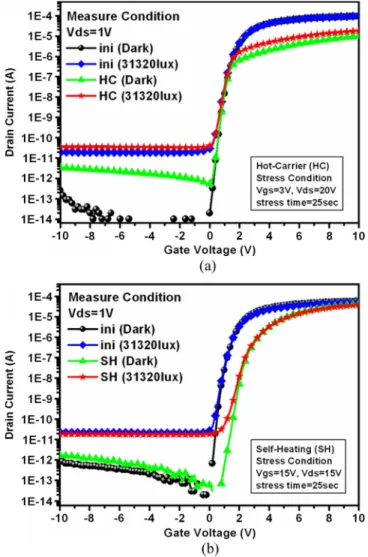
Fig. 1(a) and (b) shows the Ids–Vgs transfer characteristics of TFTs with 1-V drain voltage under different illumination conditions for hot-carrier (Vgs= 3 V, Vds= 20; 25-s stress time) and self-heating stress (Vgs= Vds= 15 V; 25-s stress time), respectively. It can be seen that the off current of the devices can be altered by both irradiation and stress.
To analyze, in detail, the photosensitivity of the poly-Si TFTs, the off current is measured at Vgs=−5 V and Vds= 1 V. Furthermore, we define the difference between off current under illumination (IDillum) and that in the dark (IDdark) as the photocurrent Iphoto, i.e., Iphoto= IDillum− IDdark. Fig. 2 shows Iphoto dependence on the illumination intensity and its error bar for those devices before and after 25 s of hot-carrier or self-heating stress. All Iphoto’s are proportional to the amount of radiant illumination (L). Thus, the sensitivity can be
2 IEEE ELECTRON DEVICE LETTERS
Fig. 1. Ids–Vgstransfer characteristics with 1-V drain voltage before and
after (a) hot-carrier stress (Vgs= 3 V, Vds= 20; 25-s stress time) and
(b) self-heating stress (Vgs= Vds= 15 V; 25-s stress time) under illumination
of 31320 lux and in the dark with the conventional forward connection.
expressed by the slope as S = dIphoto/dL. We first notice that the slope is changed oppositely by different stress conditions. It increases in the case of hot carrier, while it decreases for the self-heating case. It demonstrates that the defects play an important role on the photosensitivity behaviors of LTPS TFTs. The information of the defects can be revealed by the turn-on characteristics with forward and reverse cturn-onfiguratiturn-ons in saturation region. Therefore, we try to compare the device parameters extracted from on and off regions.
Fig. 3(a) shows photosensitivity (S) and effective mobil-ity (Mu) with forward and reverse measurements in the satu-ration region (Vd= 10 V) in accordance with stress time for hot-carrier stress. The effective mobility decreases drastically with stress time under reverse measurement, which indicates that the damaged region is near the drain. The mobility decrease is related to the increase of the tail states [6]. This trend is symmetric to the photosensitivity under forward measurement. Similarly, the effective mobility is almost no difference with stress time under forward measurement, which reflects that the nondegraded source region keeps the reverse sensitivity unchanged. The results depict that the number of tail states in the drain region affects the photosensitivity of LTPS TFT.
Fig. 2. Illumination dependence of the off currents and its error bar change before and after 25 s of hot-carrier and self-heating stress.
Fig. 3. (a) Photosensitivity and effective mobility with forward and reverse measurements in saturation region (Vgs=−5 V, Vds= 10 V) in accordance
with hot-carrier stress time and (b) photosensitivity and threshold voltage in accordance with self-heating stress time.
On the other hand, photosensitivity (S) and threshold volt-age (Vth) in accordance with the self-heating stress time are shown in Fig. 3(b). Photosensitivity decreases with long stress time for both forward and reverse measurements, while their
TAI et al.: DEPENDENCE OF PHOTOSENSITIVE EFFECT ON THE DEFECTS CREATED BY DC STRESS 3
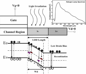
Fig. 4. Proposed model of photo-induced current mechanism for LTPS TFTs.
corresponding threshold voltage increases. Because the thresh-old voltage shift is related to the increase of the deep states, we infer that the photosensitivity can decrease, owing to the increase of dangling bonds acting as the recombination centers. It is noticed that, for the first 5 s, the reverse photosensitivity in-creases, which indicates that self-heating stress can also create defects to generate carriers.
A model of the photo-induced current for LTPS TFTs is proposed, as shown in Fig. 4, to explain the roles of defects in hot-carrier and self-heating stress. The power spectrum of the light source in the range of 350–750 nm is shown in the inset. When the LTPS TFT devices after hot-carrier stress are in forward configuration and under optical illumination, the numerous electron–hole pairs from additionally created tail states are generated in the depletion region near the drain. Therefore, the photo-leakage current obviously increases due to the photo-induced carriers from the extra states created. In reverse measurement, the damaged region is changed to the source, and the undamaged source region is changed to be the new drain. In such a case, the depletion region near the new drain covers as many defects as the device before stress. Thus, the photosensitivity remains unaltered.
The self-heating stress induces the high temperature in the poly-Si film, releasing hydrogen and leaving plenty of dangling bonds as deep states. These deep states near midgap can capture the electrons and holes generated by irradiation. Even though the photo-induced carriers might also increase due to the extra defects, the total current is eventually reduced because of the much more deep states. The sensitivity decrease in the forward measurement is more obvious than that in the reverse case. It reveals that the damage in the drain region by self-heating stress is more severe than that in the source region, consequently. This result is consistent with our previous study with electrical analysis [6]. The defect center behaviors, which influence the photo-leakage current, are extremely related to the energy level of trap defects.
IV. CONCLUSION
In this letter, we correlate the photosensitivity with different types of defects by electrical stress on the LTPS TFTs. A model is proposed to explain the illumination behaviors corresponding to the defects near the drain region. The photosensitivity can be higher if there are more tail states, while it exhibits a negative dependence on the number of deep states. This analysis allows us to understand the hot-carrier and self-heating effects and the role of defects in the photocurrent in a mutual way. It also provides the important information for the further development of using LTPS TFTs as photosensors.
REFERENCES
[1] Y. H. Tai, C. C. Pai, B. T. Chen, and H. C. Cheng, “A source-follower type analog buffer using poly-Si TFTs with large design windows,” IEEE
Electron Device Lett., vol. 26, no. 11, pp. 811–813, Nov. 2005.
[2] F. Matsuki, K. Hashimoto, K. Sano, D. Yeates, J. R. Ayres, M. Edwards, and A. Steer, “Integrated ambient light sensor in LTPS AMLCDs,” in Proc.
Soc. Inform. Display, 2007, pp. 290–293.
[3] H. S. Lim and O. K. Kwon, “Ambient light sensing circuit using LTPS TFTs for auto brightness control,” in Proc. Dig. Tech. Papers 13th Int. Workshop
Active-Matrix Flat Panel Displays Devices, 2006, pp. 21–24.
[4] A. W. Wang and K. C. Saraswat, “A strategy for modeling of variations due to grain size in polycrystalline thin-film transistors,” IEEE Trans. Electron
Devices, vol. 47, no. 5, pp. 1035–1043, May 2000.
[5] T. Fuyuki, K. Kitajima, H. Yano, T. Hatayama, Y. Uraoka, S. Hashimoto, and Y. Morita, “Thermal degradation of low temperature poly-Si TFT,”
Thin Solid Films, vol. 487, no. 1/2, pp. 216–220, Sep. 2005.
[6] Y. H. Tai, S. C. Huang, C. W. Lin, and H. L. Chiu, “Degradation of the capacitance-voltage behaviors of the low-temperature polysilicon TFTs under DC stress,” J. Electrochem. Soc., vol. 154, no. 7, pp. H611–H618, 2007.