國 立 交 通 大 學
電子工程學系 電子研究所碩士班
碩 士 論 文
複晶矽應用於太陽能電池之研究與最佳化
Study and Optimization of Polycrystalline Silicon Layers for
Solar Cell Applications
研 究 生:蔡宗哲
Tsung-Che Tsai
指導教授:鄭晃忠 博士
Dr. Huang-Chung Cheng
複晶矽應用於太陽能電池之研究與最佳化
Study and Optimization of Polycrystalline Silicon Layers for
Solar Cell Applications
研 究 生:蔡宗哲 Student : Tsung-Che Tsai
指導教授:鄭晃忠 博士 Advisor : Dr. Huang-Chung Cheng
國立交通大學
電子工程學系 電子研究所碩士班
碩士論文
A Thesis
Submitted to Department of Electronics Engineering
& Institute of Electronics
College of Electrical and Computer Engineering
National Chiao-Tung University
In Partial Fulfillment of the Requirements
For the Degree of Master
In
Electronics Engineering
July, 2011
Hsinchu, Taiwan, Republic of China
中華民國 一百 年 七 月
複晶矽應用於太陽能電池之研究與最佳化
研究生:蔡宗哲 指導教授:鄭晃忠 博士
國立交通大學
電子工程學系 電子研究所碩士班
摘要
相較於現行直接利用矽晶圓製作的太陽能電池,利用薄膜複晶矽製作的太陽 能電池可有效的減低成本。但由於薄膜複晶矽的晶粒較小而造成在晶粒邊界大量 的覆合電流,以及由於厚度較薄造成較低的光吸收率,這些問題均仍待進一步研 究並克服以期能達到更有效率的薄膜複晶矽太陽能電池。其中,增加晶粒大小是 解決問題的方式之一,因其可使晶粒邊界減少以降低在晶粒邊界造成的載子覆 合,進而增進複晶矽太陽能電池的效率。直接沉積複晶矽於非矽基板上可以很容 易的得到複晶矽薄膜,但直接沉積會導致其晶粒過小而造成前述問題。因此,為 了得到較大的晶粒,已有許多不同使矽結晶的方式被研究。在本篇論文中我們利 用固相結晶法以及鋁誘發結晶法來得到我們所需的複晶矽材料。利用鋁誘發結晶 法可得到相當大的晶粒大小(1~50μm),但因為鋁誘發結晶法會使產生的複晶矽中 有鋁元素的參雜(參雜濃度約為1×1018 cm-3),同時也因為利用此法產生的複晶矽層 厚度無法達到吸收層所需厚度,因此直接利用鋁誘發結晶法並無法得到太陽能電 池的吸收層。欲製作此吸收層,則必須利用在鋁誘發結晶法生成的晶種層上做磊 晶而得到。以此法製作的優點是一方面在製作晶種層時,我們可以致力於使晶粒 大小盡可能的大而不需要考慮參雜濃度對於吸收層效能的影響,另一方面在磊晶 製作吸收層時控制我們所需的參雜濃度以期得到最好的效能。然而,利用鋁誘發 結晶法製作的晶種層因具有高密度的電活性晶粒內缺陷,而使得其太陽能電池的效率並未如預期的隨著晶粒大小增加而增加。這些缺陷的電活性推測可能是由於 機台(E-gun)中存在的銅元素汙染所造成的。因此,我們利用固相結晶法製作晶種 層以用來做不同潔淨度的比較。 我們利用兩種不同的機台來沉積固相結晶法的晶種層,除了和鋁誘發結晶法 使用相同的機台(E-gun)外,也利用較無金屬汙染可能的機台(PECVD)來沉積產生 固相結晶法的晶種層。同時,退火條件、參雜濃度等亦均以不同條件測試以期能 達到較大的晶粒大小。於本論文中晶粒大小多小於1μm。此份論文內製作的太陽能 電池主要製作於三種不同的晶種層上,此三種晶種層分別為鋁誘發結晶法製作的 晶種層、含有金屬汙染以固相結晶法製作的晶種層、以及不含有金屬汙染以固相 結晶法製作的晶種層。製作在鋁誘發結晶法晶種層上的太陽能電池擁有最高的效 能,其最高效能的轉換效率為4.7%、開路電壓為503mV、閉路電流為12.9 mA/cm2。 次者,利用無金屬汙染的固相結晶法晶種層製作的太陽能電池擁有3.5%的轉換效 率、486mV的開路電壓以及9.7 mA/cm2的閉路電流。另外,利用含有金屬汙染的固 相結晶法晶種層製作的太陽能電池的效能最低,其轉換效率為3.1%、開路電壓為 469mV、閉路電流為9.2 mA/cm2。利用鋁誘發結晶晶種層製作的太陽能電池之所以 擁有較高的效能是因為其複晶矽層具有非常大的晶粒,其晶粒大小為固態結晶法 形成之晶粒大小的二十倍。僅比較兩種由固相結晶法晶種層形成之太陽能電池時 我們發現,沒有金屬汙染的太陽能電池效能確實是優於含有金屬汙染的太陽能電 池,這是由於減少了不必要的金屬汙染而使得電活性晶粒內缺陷的數目減少進而 改善效能。 綜合以上所述,本論文證明了增加複晶矽的晶粒大小確實可以增進太陽能電 池的效率,另外,減少存在於複晶矽中不必要的金屬汙染亦可以增進太陽能電池 的效能。同時,利用在晶種層上磊晶成長的複晶矽吸收層,高轉換效率的薄膜複 晶矽太陽能電池將指日可待。
Study and Optimization of Polycrystalline Silicon Layers for
Solar Cell Applications
Student: Tsung-Che Tsai Advisor: Dr. Huang-Chung Cheng
Department of Electronics Engineering & Institute of Electronics
National Chiao Tung University
ABSTRACT
Photovoltaic solar cells based on a thin layer of polycrystalline silicon are a low-cost alternative for the current wafer-based silicon solar cells. Because of their small grain size, the large recombination current at the grain boundaries and the low absorbance of the light in the thin polycrystalline silicon layer, it is really challenging to obtain a good performance of these cells. An increased pc-Si solar cell performance is expected with increasing grain size because the number of efficient recombination centers, present at grain boundaries, decreases. Direct deposition of silicon on a non-silicon substrate however results in amorphous or small-grained material. To fulfill the demand of relatively large grains, different methods to crystallize silicon are being investigated. Two possible ways, aluminum induced crystallization (AIC) and solid phase crystallization (SPC), were adapted in this work. AIC has the advantage of promising large grains (1~50μm). But since as-formed AIC layers have an intrinsic aluminum doping density of around 1×1018 cm-3 and cannot be made thick enough, it is not possible to directly use them as the absorber layer for a solar cell. Absorber layers can however be obtained by epitaxial thickening of the AIC seed layers. Here we call it two step process which represents the method we formed our pc-Si layer. By using this two step process, we can grow larger grain sizes and solely control our crystalline property without considering the effect of doping concentration which is needed in the absorption layer of solar cell. However, the high density of electrically active intra-grain
defects present in the AIC seed layer makes the solar cell performance quasi independent with the grain size. These electrically active intra-grain defects were caused by the possible copper contamination existing in our system during seed layer deposition. This problem has no clear way to solve yet. Thus, the SPC seed layers were made as a comparison with the AIC seed layers.
Different deposition equipments (with or without possible metal contamination), annealing conditions and doping levels were investigated in this work in order to maximize the grain size (<1μm) of SPC seed layers. We fabricated our solar cells on mainly three different types of seed layer, namely AIC with metal involved, SPC with metal contamination involved, and SPC with metal contamination not involved. The solar cells made on the AIC seed layers have the highest efficiency about 4.7% with open circuit voltage of 503 mV and short circuit current of 12.9 mA/cm2 in this work. This superior performance over solar cells made on SPC seed layers were due to the much larger grain sizes of its polycrystalline silicon body even though metal contamination was involved. The efficiency was 3.5% with open circuit voltage of 486 mV and short circuit current of 9.7 mA/cm2 for the solar cells fabricated on SPC seed layers with metal contamination not involved. And the efficiency was 3.1% with open circuit voltage of 469 mV and short circuit current of 9.2 mA/cm2 for the solar cells fabricated on SPC seed layers with metal contamination involved. From these values we can see that the performance of solar cells made on SPC seed layers which were metal contamination not involved showed better results than those metal contamination involved. This improvement of the performance is because of the limitation of unwanted metal contaminations among the pc-Si layer, thus reduce the amounts of electrically active intra-grain defects.
To sum up, this work has proved that increasing the grain size of pc-Si layers can improve the solar cell performance. Also, limitation of unwanted metal contaminations in the pc-Si seed layer can improve the performance of our pc-Si solar cells. As a result, with the two step process (seed layer and epitaxial growth), large grain thin film pc-Si solar cell with high efficiency could be expected
誌 謝
感謝我的論文指導教授 鄭晃忠博士、 Robert Mertens 博士與 Jozef Poortmans 博士在實驗、研究與論文上熱心詳實的指導,老師們嚴謹認真的研究態度以及謙 恭溫和的待人處事,皆讓學生獲益匪淺,特別是 鄭晃忠博士對於申請比利時魯汶 大學雙聯碩士的支持與鼓勵,讓我有這個機會到國外的大學體驗不一樣的環境與 學習,進而順利完成碩士學位。
感謝逸哲學長、柏宇學長、加聰學長、昭龍學長、明哲學長、Dries Van Gestel
博士、Srisaran Vancatachalem 學長、雋荃同學在研究與實驗上的指導與惠見,讓我 從原本對無塵室環境一切陌生的狀態下一步步地學會各項實驗技術,也漸漸掌握 到論文研究的方法與方向,由衷地感謝您們。 感謝交大實驗室的學長姐、同學以及在IMEC 的團隊─俊諭學長、宏顯學長、 昱智學長、加聰學長、萬霖學長、筠珊學姐、旭航同學、晏廷同學、Ivan Gordon 博士、邱瑜博士、 Valerie Delpauw 博士在各方面提供的協助與鼓勵,由於您們 在生活上的陪伴和打氣,讓我這一路走來更加輕鬆愉快。 感謝國立交通大學奈米中心、國家奈米元件實驗室以及 IMEC 的所有行政人 員、研究員、工程師及技術員提供優良的製程設備與研究環境,讓我的研究實驗 得以順利完成。 感謝我最親愛的父母:蔡文正先生與張惠蓉女士,因為有您們從小到大無微 不至的關懷與照顧,也總對自己選擇的方向和興趣表以支持和鼓勵,使我終能有 今日的成績,願將完成碩士學位論文之喜悅與您們分享。 感謝林辰筠小姐,這段期間有妳貼心的陪伴也總在我低潮時給我鼓勵。 感謝在這兩年來曾經幫助或鼓勵過我的人,雖然沒有一一寫出您們的名字, 但我從未忘記對您們的感謝,衷心的感激您們。
Contents
Abstract (in Chinese) ... i
Abstract (in English) ... iii
Acknowledgements (in Chinese) ... v
Contents ... vi
Table Lists ... ix
Figure Captions ... x
Chapter 1 Introduction ... 1
1.1 Overview of Thin-Film Polysilicon Solar Cells ... 1
1.2 Overview of Crystallization of Amorphous Silicon Thin Films ... 3
1.2.1 Solid Phase Crystallization of Amorphous Silicon Thin Films ... 4
1.2.2 Metal Induced Crystallization of Amorphous Silicon Thin Films ... 5
1.2.3 Laser Crystallization of Amorphous Silicon Thin Films ... 6
1.3 Motivation ... 7
1.4 Thesis Organization ... 8
Chapter 2 Fabrication of Thin Film Polycrystalline Silicon Solar Cells ... 10
2.1 Process Overview ... 10
2.2 Substrate Preparation ... 12
2.3 Seed Layer Formation ... 14
2.3.1 Solid Phase Crystallization ... 14
2.4 Epitaxial Growth ... 17
2.5 Solar Cell Fabrication ... 18
2.5.1 Hydrogenation ... 18
2.5.2 Emitter Formation ... 19
2.5.3 Contact Formation ... 20
Chapter 3 Results and Discussion ... 23
3.1 Introduction ... 23
3.2 SPC Seed Layers Prepared by E-gun Evaporation ... 24
3.2.1 P-type Doping Seed Layers ... 24
3.2.1.1 Crystallographic Properties ... 24
3.2.1.2 Electrical Properties ... 27
3.2.2 Intrinsic Seed Layers ... 28
3.2.2.1 Crystallographic Properties ... 28
3.2.2.2 Electrical Properties ... 29
3.3 SPC Seed Layers Prepared by PECVD ... 29
3.3.1 Crystallographic Properties ... 30
3.3.2 Electrical Properties ... 31
3.4 Comparison of the Crystallization Behavior between SPC Seed Layers ... 32
3.5 AIC Seed Layers ... 34
3.5.1 Crystallographic Properties ... 34
3.6 Epitaxial Grown Layers ... 35
3.7 Characterization of Solar Cells Fabricated on AIC and SPC Seed Layers ... 35
3.7.1 Metal Contamination Involved ... 37
3.7.2 Metal Contamination not Involved ... 38
3.7.3 Comparison between Metal Contamination Involved and not Involved ... 38
Chapter 4 Summary and Conclusions ... 40
References ... 70
Table Lists
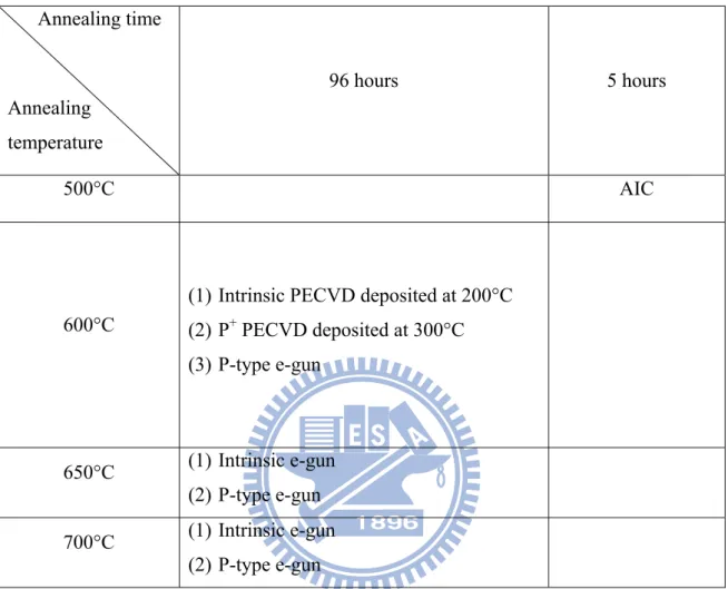
Table 3-1 Crystallization results of e-gun deposited a-Si annealing at several different temperatures for 96 hours. The criteria based on whether there are grain orientation peaks appear on X-ray diffraction measurement ... 42 Table 3-2 Crystallization results of a-Si deposited at 200°C and 300°C by PECVD. The annealing process was carried out for 96 hours at 600°C, 650°C, and 700°C.42 Table 3-3 Results of Hall effect measurement on the p+ pc-Si seed layer (deposited at 300°C by PECVD and annealing at 600°C for 96 hours). ... 43 Table 3-4 Tcryst values for the in-situ XRD measurement. Tcryst is defined as the max of
the second derivative from summed intensity versus ramping temperature. .. 43 Table 3-5 Results of Hall effect measurement on the AIC seed layer. ... 43 Table 3-6 The seed layers listed here are chosen to make epitaxial growth absorber
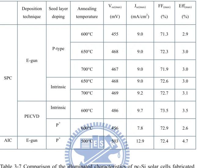
layers for solar cells. ... 44 Table 3-7 Comparison of the illuminated characteristics of pc-Si solar cells fabricated on different seed layers. The values shown in this table are the best results. . 45 Table 3-8 The illuminated characteristics of pc-Si solar cell fabricated on fine grain
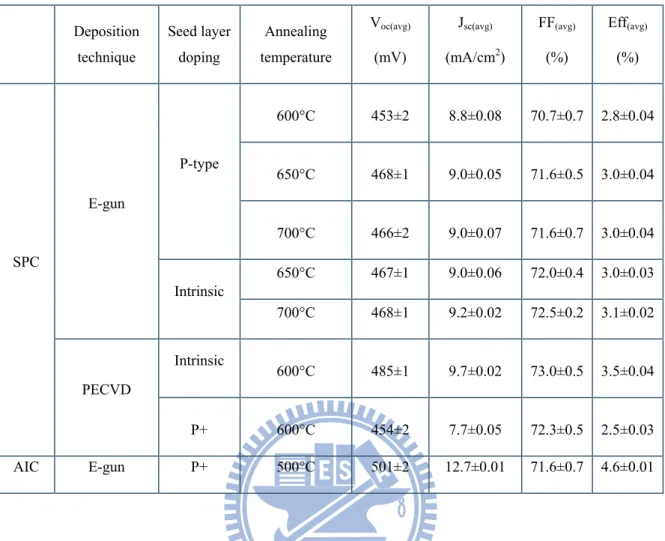
pc-Si without a seed layer. The values shown in this table are the best rsults.45 Table 3-9 Comparison of the illuminated characteristics of pc-Si solar cells fabricated on different seed layers. The values shown in this table are average values and the standard deviation from this work. ... 46 Table 3-10 The illuminated characteristics of pc-Si solar cell fabricated on fine grain
pc-Si without a seed layer. The values shown in this table are the average values and the standard deviation from this work.. ... 46
Figure Captions
Chapter 2
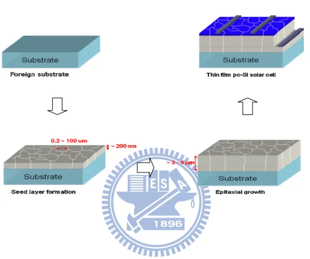
Fig. 2-1. Schematic picture of the process flow for the two step thin film polycrystalline silicon solar cell. (a) Preparation of foreign substrates. (b) Polycrystalline silicon seed layer formation. (c) Epitaxial growth on the seed layer. (d) Fabrication of the thin film polycrystalline silicon solar cell. ... 47 Fig. 2-2. Schematic picture of the solid phase crystallization process flow for seed layer formation. (a)Preparation of foreign substrates. (b)Deposition of amorphous silicon layer on a foreign substrate. (c)After annealing of the amorphous silicon layer, the amorphous silicon was converted into polycrystalline silicon. ... 48 Fig. 2-3. Schematic picture of aluminum induced crystallization process flow for seed
layer formation. (a) Deposition of aluminum and amorphous silicon stacked layer on a foreign substrate. (b) Anneal the stacked layer. (c) Remove the top aluminum layer after annealing. ... 49 Fig. 2-4. (a) Cross section of interdigitated thin-film Si solar cells. (b) Top view of
interdigitated contacts. ... 50
Chapter 3
Fig. 3-1. XRD graph of p-type e-gun deposited a-Si after annealing for 96 hours at 700°C (green line), 650°C (black line), 600°C (red line), and as-deposited a-Si (blue line). ... 51 Fig. 3-2. XRD graph of p-type e-gun deposited a-Si after annealing at 700°C for 96
Fig. 3-3. TEM picture of p-type e-gun deposited amorphous silicon layer after annealing at 600°C for 96 hours. (a) The whole amorphous silicon layer was 480 nm. Only the bottom 100 nm was crystallized, the other 380 nm on top remained in amorphous state. (b) Zoom in to the bottom 100 nm. ... 52 Fig. 3-4. TEM pictures of intrinsic e-gun deposited amorphous silicon layer after
annealing at 700°C for 96 hours. (a) The whole layer was 480 nm and was fully crystallized. (b) Lots of defects exist in the layer ... 53 Fig. 3-5. Resistivity versus inverse temperature plots of p-type e-gun deposited a-Si
after annealing for 96 hours at 600°C (red line), 650°C (black line), and 700°C (green line). ... 54 Fig. 3-6. XRD graph of intrinsic e-gun deposited a-Si after annealing for 96 hours at
700°C (green line), 650°C (black line), 600°C (red line), and as-deposited a-Si (blue line). ... 54 Fig. 3-7. XRD graph of intrinsic e-gun deposited a-Si after annealing at 600°C for 96
hours (red line) and 173 hours (purple line). ... 55 Fig. 3-8. XRD graph of intrinsic e-gun deposited a-Si after annealing at 700°C for 96 hours (green line), 48 hours (black line), and 24 hours (red line). ... 55 Fig. 3-9. Resistivity versus reverse temperature plots of intrinsic (red lines) and p-type (blue lines) e-gun deposited a-Si after annealing for 96 hours at 700°C (with circle marks) and 650°C (with triangle marks). ... 56 Fig. 3-10. Pictures of n-type a-Si deposited at 200°C by PECVD after annealing at
600°C for 24 hours. Serious peeling off phenomenon can be seen all over the surface. The left picture is a whole image of a 5 cm by 5 cm sample. The
right picture is the zoom in.. ... 56 Fig. 3-11. XRD graph of p+ (green line) and intrinsic a-Si deposited by PECVD at
300°C (black line) and 200°C (red line) after annealing at 600°C for 96 hours. Blue line shows the as-deposited a-Si... 57 Fig. 3-12. TEM picture of intrinsic PECVD deposited amorphous silicon layer after
annealing at 600°C for 96 hours. (a) The whole layer was 420 nm and was fully crystallized. (b) Lots of defects exist in the layer. ... 58 Fig. 3-13. XRD graph of intrinsic a-Si deposited at 200°C by PECVD after annealing at 600°C for 96 hours (green line), 48 hours (black line), 24 hours (red line), and 12 hours (blue line). ... 59 Fig. 3-14. XRD graph of intrinsic a-Si deposited at 300°C by PECVD after annealing at 600°C for 96 hours (green line), 48 hours (black line), 24 hours (red line), and 12 hours (blue line). ... 59 Fig. 3-15. XRD graph of p+ a-Si deposited at 300°C by PECVD, annealing at 600°C for 96 hours (green line), 48 hours (black line), 24 hours (red line), and 12 hours (blue line). ... 60 Fig. 3-16. Resistivity versus reverse temperature of PECVD deposited a-Si after
annealing at 600°C for 96 hours. The black line represents the intrinsic sample deposited at 300°C. The red line represents the intrinsic sample deposited at 200°C. The green line represents the p+ sample deposited at 300°C. ... 61 Fig. 3-17. Resistivity vs. reverse temperature of intrinsic samples annealing for 96 hours.
700°C (green line), and 600°C annealed PECVD samples deposited at 300°C (blue line) and 200°C (red line) are showed. ... 61 Fig. 3-18. Summed intensity versus ramping temperature derived from in-situ XRD [34].
The black line represents the peak intensity at (220) orientation, and the red line represents the (311) orientation. (a) intrinsic e-gun, (b) p-type e-gun, (c) intrinsic PECVD (deposited at 200°C), (d) p-type PECVD (deposited at 200°C). ... 62 Fig. 3-19. XRD graph of the AIC seed layer. ... 63 Fig. 3-20. IPF EBSD measurements (using the Z direction perpendicular to the sample surface) of AIC seed layers. The areas of 80×80 μm2 were examined with a step size of 0.1 μm. ... 63 Fig. 3-21. Resistivity versus reverse temperature plots of the AIC seed layer. ... 64 Fig. 3-22. XRD graph of the epitaxial growth layer grown on SPC seed layer. The SPC seed layer is p-type e-gun evaporated a-Si layer annealing at 700°C for 96 hours. ... 64 Fig. 3-23. XRD graph of the epitaxial growth layer grown on AIC seed layer. The AIC
seed layer was annealing at 500°C for 5 hours. ... 65 Fig. 3-24. Illuminated current voltage curve of the best pc-Si solar cell in this work
made on p-type e-gun seed layer which was annealed at 700°C for 96 hours.65 Fig. 3-25. Illuminated current voltage curve of the best pc-Si solar cell in this work
made on p-type e-gun seed layer which was annealed at 650°C for 96 hours.66 Fig. 3-26. Illuminated current voltage curve of the best pc-Si solar cell in this work
made on p-type e-gun seed layer which was annealed at 600°C for 96 hours.66 Fig. 3-27. Illuminated current voltage curve of the best pc-Si solar cell in this work
made on intrinsic e-gun seed layer which was annealed at 650°C for 96 hours. ... 67 Fig. 3-28. Illuminated current voltage curve of the best pc-Si solar cell in this work
made on intinsic e-gun seed layer which was annealed at 600°C for 96 hours. ... 67 Fig. 3-29. Illuminated current voltage curve of the best pc-Si solar cell in this work
made on p+ PECVD seed layer which was annealed at 600°C for 96 hours. ... 68 Fig. 3-30. Illuminated current voltage curve of the best pc-Si solar cell in this work
made on intrinsic PECVD seed layer which was annealed at 600°C for 96 hours. ... 68 Fig. 3-31. Illuminated current voltage curve of the best pc-Si solar cell in this work
made on AIC seed layer which was annealed at 500°C for 5 hours. ... 69 Fig. 3-32. Illuminated current voltage curve of the pc-Si solar cell made on fine-grain pc-Si without a seed layer. ... 69
Chapter 1
Introduction
1.1 Overview of Photovoltaic Energy and
Thin-Film Polycrystalline Silicon Solar
Energy
The world is becoming tremendously aware of the significant problems associated with global warming, such as frequent and intense heat waves, cold waves, floods, droughts and storms. A major contribution to global warming comes from greenhouse gas emissions such as carbon dioxide. Nuclear based energy resource is a powerful and economically preferable, but it is also well known for its risks and hence it does not seem to be suitable for worldwide use. As an alternative, people have been developing various kinds of carbon-free, sustainable and renewable energies such as wind power, hydro-power, bio-mass, geothermal, solar thermal and photovoltaic energy. Although most of these energies are still more expensive than fossil fuel, it is deemed that these will make a large contribution to the worldwide energy supply in the middle to long
term by reducing the dependence on fossil fuels.
Photovoltaic cells (PV) are made up of semiconductor material that converts solar radiation into electricity. Photovoltaic energy has a number of advantages such as its excellent scalability, noiseless, applicable at remote areas low maintenance operation, and temporal peak load matching, especially in countries with heavy use of air-conditioners. Today’s PV market is dominated by solar cells based on mono and multi crystalline silicon wafers of 200 – 500 µm thick. However, practically, only several microns of the silicon are used to convert the sunlight into electricity, representing a significant waste of expensive silicon material. The efficiency of the device has to be increased which is naturally attempted in all silicon based solar cell concepts but is limited to 30% for an energy gap of 1.1 eV as pointed out by W. Shockley and H.J. Queisser [1]. M. Green summarized ideas on how to overcome this theoretical limit with so called third generation solar cells [2]. The most promising approach on a short to middle term for solar cells to reduce material consumption is the reduction of the cell thickness. Thin film concepts are considered second generation PV [3]. Unfortunately, being limited by the sawing loss and other technical problems, it is not possible to simply cut the silicon ingots into thinner and thinner wafers. As a consequence, a less material intensive technology “a thin-film technology“ seems necessary for a large-scale terrestrial application of PV.
Polycrystalline silicon (pc-Si) with its promising properties is one of the candidates of the thin-film PV devices [4]. A thin-film pc-Si solar cell is made of a thin pc-Si layer on top of a foreign substrate. A pc-Si solar cell has no degradation effect as a-Si and μc-Si solar cells. In order to minimize recombination at grain boundaries, a large grained pc-Si is desirable. A large grain can be defined as a grain which is laterally
larger than its layer thickness. In this case the efficiency is more limited by the recombination at the front and back contacts than small grain cells. The pc-Si solar cells are hoped to yield efficiencies comparable with the wafer based solar cells at much lower cost.
1.2 Overview of Crystallization of Amorphous
Silicon Thin Films
The crystallinity of pc-Si thin film has great influence on the performance of thin film pc-Si solar cells. For a pc-Si thin film, the grain boundaries cause a lot of defects, which is so called strained bonds and dangling bonds. These defects act as trap states within the band gap and will degrade the performances of pc-Si solar cells, such as open circuit voltage, fill factor, and efficiency. Furthermore, the defects in pc-Si solar cells could result in many reliability issues. It is generally believed that enlarging the grain size and reducing the defect density are the most important key technologies to obtain high quality pc-Si thin films. Enlarging the grain size and reducing the defect density in pc-Si could make it approach the quality of single-crystalline silicon, which could result in a better performance of pc-Si devices. As a result, it is important to control the grain size and grain boundaries to fabricate high quality pc-Si thin films. Recently, various methods, such as solid phase crystallization (SPC), metal induced crystallization (MIC), and laser crystallization, have been proposed for a-Si crystallization on glass material, which could be concluded that the a-Si thin films are re-crystallized into pc-Si thin film by additional energy. These kinds of low
temperature crystallization methods will be roughly reviewed in the following three sections.
1.2.1 Solid Phase Crystallization of Amorphous Silicon Thin
Films
Silicon thin films deposited in the amorphous structure and then crystallized into the polycrystalline structure have been shown to have higher carrier mobility since the larger grain size compared to the direct-deposited pc-Si thin films [5]. Solid phase crystallization is a simple method to convert a-Si thin films into pc-Si thin films with large grains via furnace annealing by thermal energy for 24 hours at temperature of 600°C. With different annealing temperature and annealing time, the crystallinity of derived pc-Si thin film could be different.
Generally, the solid phase crystallization involves two distinct processes, the nucleation of seeds and grain growth into final polycrystalline silicon films [6]. The transformation proceeds within the amorphous matrix after an apparent incubation period by the nucleation and dendritic-like growth of crystal domain, and the final grain size could be larger if the nucleation rate is low and the grain growth rate is high [7]. Furthermore, the surface morphology is much smoother in the solid phase crystallization polycrystalline silicon thin films than in the as-doped ones. Despite the long crystallization durations of several tens of hours, large defect density still exists in the crystallized polycrystalline silicon thin films due to the low temperature process.
1.2.2 Metal Induced Crystallization of Amorphous Silicon
Thin Films
Metal induced crystallization (MIC) is a method to lower the process temperature (<500°C) and shorten the process duration (<5hrs) of solid phase crystallization by introducing certain metal impurities [8]-[10]. The reaction between the metal and amorphous silicon occurs at an interlayer by diffusion and lowers the crystallization temperature. The enhancement of crystallization is due to an interaction of the free electrons from the metal with covalent Si bonds near the growing interface.
Recently, several metals have been proposed to realize the MIC process, such as aluminum (Al), aurum (Au), platinum (Pt), and nickel (Ni), etc. Among various metals, Al has been chosen for creating pc-Si thin films for thin film pc-Si solar cells due to its promising very large grains (1 – 100μm) and the low processing temperature [11]. This process is also called aluminum induced crystallization (AIC). When Al is deposited on a-Si, electronic screening weakens the covalent bonds of the a-Si, facilitating the diffusion of Si atoms into the metal film during heating, where the Si atoms will find some preferred nucleation sites at the metal grain boundaries. Because of the continuous supply of Si atoms, the Si grains will continue to grow at these sites until they contact each other and form a continuous film which ultimately results in layer inversion. For Al, this process can start immediately because of the solubility of Si in the metal film while the solubility for Ag is negligible even at elevated temperatures of 1350°C. More detail, considering the temperature of metal-Si eutectic, a-Si thin film can be crystallized below 500°C.
1.2.3 Laser Crystallization of Amorphous Silicon Thin Films
Laser crystallization has been receiving considerable attention in fabrication of silicon-on-insulator devices for microelectronics and thin-film transistors for displays [12]. Laser crystallization can produce pc-Si thin film low density of intra-grain defects. The laser crystallization is a liquid phase crystallization process which is contrast to above discussed two solid phase crystallization process such as SPC and MIC. Therefore, many studies in laser crystallization of a-Si films have been using various kinds of laser techniques, such as CO2, Ar, Nd:YAG, Nd:YVO4, excimer, andfemtosecond lasers[13][14].Among these laser techniques, excimer laser annealing is the widely used to prepare pc-Si thin films thanks to its high pulsed-laser power and the large absorption coefficient for a-Si in the UV light region. According to the gas mixture used in the laser tube, excimer laser radiation of output wavelengths between 157 - 351 nm were obtained by the transient high voltage discharge with short pulse duration.
Another unique advantage of lasers is the strong optical absorption of UV light in silicon. As a result, most of the incident laser energy is absorbed close to the surface of the thin film without causing severe thermal strain on the substrate. The strong optical absorption of the UV light in silicon and short pulse duration of the excimer laser imply that high temperature can be produced in the silicon surface region, causing rapid melting and solidification, without significant heating of the substrate. This avoids diffusion of impurities from the substrate into the silicon thin film. This technology yield high quality and large-grained pc-Si thin film for high-performance pc-Si TFTs on glass or plastic substrate with high throughput. Owing to the advantageous features of excimer laser crystallization for large area microelectronics fabrication, many studies
have been done to understand the dynamic kinetics and transformation mechanisms of the laser crystallization of a-Si thin films. The characteristics of pc-Si thin film are related to the process conditions of laser crystallization, such as laser energy density, pulse duration, number of shots per unit area, crystallization ambient, and substrate temperature. Moreover, the initial conditions of a-Si precursor film has a profound effect on the properties of the resulting pc-Si film, including thickness, hydrogen and impurity content of a-Si film [12]-[15].
1.3 Motivation
A promising approach to make large grain pc-Si films on foreign substrates was the epitaxial thickening of seed layers made by AIC of amorphous silicon [16]. By using the seed layer, we can grow larger grain size and solely control our crystalline property without considering the effect of doping concentration which is needed in the absorption layer of solar cell. However, the grain size enlargement did not result in promising increasing solar cell performance [16] [17]. The reason for the independent solar cell performance with varying grain size may probably caused by the present of the large amounts of electrically active intra-grain defects [17] [18]. In order to further investigating in such phenomenon, the seed layer formed by SPC is carried out in this work. The a-Si deposition for SPC was done in two different systems, e-gun evaporation and PECVD. With e-gun evaporation system, the same contamination level with the AIC formed pc-Si was expected the same since they were done by the same system. The one deposited by PECVD was regarded as without such contamination due to the higher cleaning level of the system. Also, the SPC pc-Si grain size is much smaller than AIC
pc-Si. By comparing the cell performance between these two kinds of SPC pc-Si and AIC pc-Si, we can see the effect of grain size and whether the electrically active intra-grain defects dominate the effect of cell performance or not.
1.4 Thesis Organization
In chapter 1, a brief overview of PV energy and thin film pc-Si solar cells were shown. An overview of crystallization processes of a-Si were generally described in the subsequent section. The motivations of this thesis were subsequently explained to introduce this thesis.
In chapter 2, practical experimental details were carried out. First, an overall process overview was shown as an introduction for the whole thin film pc-Si solar cell process. Benefits of the two step process to form the thin film pc-Si layer were emphasized here. Next, the substrate preparation was described to show how we chose our substrates. Then the seed layer formation process was introduced, including SPC and AIC methods. Also, the epitaxial growth and the solar cell fabrication process, including hydrogenation, emitter formation, and contact formation, were shown in this chapter.
In chapter 3, some results from this work were introduced and further discussed. A general introduction about the results was introduced as the beginning. Next, various seed layers were investigated, including SPC seed layers prepared by e-gun evaporation, SPC seed layers prepared by PECVD, and AIC seed layers. Both crystallographic properties and electrical properties were investigated in this work for all the seed layers. The crystallographic characterization results, including X-ray diffraction (XRD),
transmission electronic microscope (TEM), and optical microscope were shown here. And the electrical characterization results, including resistivity versus temperature and Hall affect measurement were also shown in this chapter. After the seed layers characterization, some results of epitaxial layers were also introduced. Then the final results of solar cells were also shown in the last section of this chapter.
Chapter 2
Fabrication of Thin Film Polycrystalline
Silicon Solar Cells
2.1 Process Overview
Different technologies of fabricating a thin film pc-Si solar cell are investigated. The challenge is to obtain a high quality pc-Si layer on non silicon substrates. The electrical quality of a pc-Si can be improved by increasing grain size/decreasing number of grain boundaries. Direct deposition of silicon on non silicon substrate results in small grained material. To obtain larger grains, a seed layer + epitaxial growth two step process to form the pc-Si absorber layer can be used. By using the seed layer, we can grow larger grain size and solely control our crystalline property without considering the effect of doping concentration which is needed in the absorption layer of solar cell. Fig. 2-1 shows the general process flow of a two step pc-Si solar cell. A brief overview of the whole process and each step is discussed in detail as follows.
(a) Foreign substrate
The pc-Si solar cells use silicon layer of 2–6 μm thick. This pc-Si layer is not self-supporting and therefore, a foreign substrate is used to enhance its mechanical strength. An appropriate substrate is chosen and it needs to fulfill certain requirements like thermal stability, matched CTE to be compatible with the deposition process and to be economical compatible [19].
(b) Seed layer formation
The seed layer here is a thin (~200nm) layer of pc-Si as a starting point for the next epitaxial step. By using the seed layer, we can grow larger grain size and solely control our crystalline property without considering the effect of doping concentration which is needed in the absorption layer of solar cell. Different technologies exist to prepare a thin pc-Si layer as mentioned in chapter 1. Thus, this seed layer can be obtained through several crystallization methods, namely SPC, MIC, and laser crystallization. In this work, we mainly focus on AIC and SPC. Low aspect-ratio grains are possible to obtain. The experimental description of these two processes is detailed in section 2.2, and the results will be shown in Chapter 3.
(c) Epitaxial growth
The seed layer is epitaxially thickened by atmospheric pressure CVD. The grown pc-Si is the back surface field and base or absorber layer of the solar cell. Since the crystalline structure are already determined by the seed layer, here we can control the layer thickness and doping type and doping level without concerning the dopants will effect crystallization process. The final grain diameter is determined by the seed layer.
Epitaxial growth is possible with different techniques and a wide temperature range. In this work, high temperature CVD is used as will be described in section 2.3.
(d) Solar cell fabrication
We prepare solar cells on the deposited pc-Si layer. It involves several steps. Hydrogenation is the first step after the pc-Si formation. After hydrogenation, the n-type emitter was deposited since we have a p-type poly-Si absorption layer. As a final processing step, metal contacts are created to deliver the generated power to the external world. Each of these steps will be described in detail in section 2.4.
2.2 Substrate Preparation
Thermal stability: the substrate must be stable towards the at temperatures of the deposition (~ 1130 ºC). Standard inexpensive glasses used for amorphous and microcrystalline Si solar cells, such as soda lime glass, cannot be used at these deposition temperatures due to their too low softening temperature (~ 575 ºC). Even the more stable borosilicate glasses used in solid phase crystallization cannot be used because of thermal stability problems (softening temperature ~ 820 ºC).
Optical properties: Thin-film crystalline solar cells allow in principle to maintain high efficiencies while using very thin active layers. However, this is only possible if efficient light confinement is applied. This requires a good light reflection at the interface between the Si layer and the substrate on one hand and a scheme to give light rays an oblique path on the other hand.
Impurity content: It is well documented that many impurities have detrimental effect on the performance of Si solar cells. In particular, most metallic impurities start to be harmful already at trace concentrations. When we deposit Si at high temperature on a foreign material, an important concern therefore is the possible contamination of the layer by solid state diffusion of impurities from the substrate. These contaminants can either be elements from the main components of the substrate material or other species present as impurities in the material. The need for a barrier layer or clean step therefore has to be reassessed for each newly developed material.
Coefficient of Thermal Expansion(CTE): After epitaxial deposition, the substrate needs to cool down from deposition temperature to room temperature. During cooling down, the substrate and the silicon layer contract and mechanical stress develops due to CTE mismatch. This results in deteroitaion of the films. Therefore, the second requirement is that the thermal expansion coefficient of the substrate is as close as possible to the one of silicon (~ 4.2×10⁻⁶ K-1). Metal substrates such as stainless steel can be cost-effective, however their thermal expansion coefficients is usually much higher (thermal expansion coefficient of stainless steel ~ 12×10-6 K-1).
Economically cheap substrate: The third and most important requirement is the economical compatibility of the substrates. This means, the substrates should be produced in large amounts at a low cost.
Oxidized silicon wafers are used as a model for a foreign substrate in this work. They are obtained by wet oxidation of a monocrystalline silicon wafer. The oxide layers are typically around 1.5 μm thick. They are not considered as suitable for industrial production, since they are expensive bulk silicon wafers. However for practical reasons they were used for fast depositions of pc-Si to optimize the process in this work.
2.3 Seed Layer Formation
Direct deposition of pc-Si layers have the advantage of simple processing step but suffer from the small grain size resulting in a large number of defects, where recombination between minority and majority carriers can occur. An obvious strategy to reduce the number of defects in the pc-Si layers is to enlarge the grain size of the material. Due to a larger grain size, less grain boundaries are obtained and one can expect a better electronic quality of the material with less carrier recombination at the grain boundaries. In this work, SPC and AIC are used to form the seed layer on foreign substrate as described as follows.
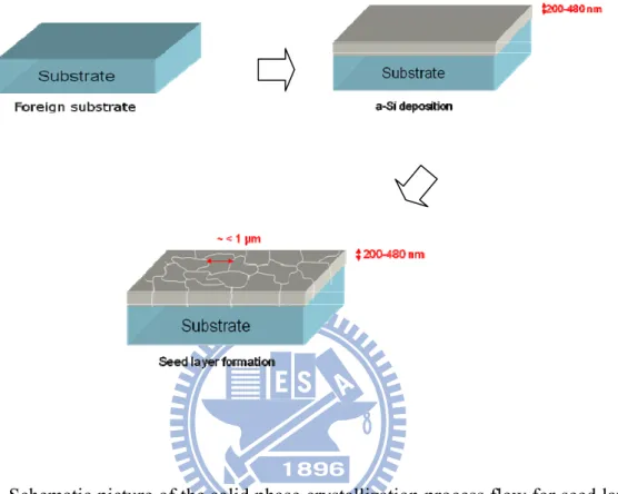
2.3.1 Solid Phase Crystallization
As previously shown in Fig. 2-1 the first process step is obtaining a pc-Si seed layer. Fig. 2-2 shows schematically the various steps to obtain a seed layer based on SPC.
oxidized wafer as shown in Fig. 2-2 (a, b). The thick layer is used only for easier measurement. Two different deposition techniques, high vacuum e-gun evaporator and Plasma Enhanced Chemical Vapor Deposition PECVD were used in this work. The a-Si layer deposited by e-gun system is regarded as a dirty one since there are some metal contaminations. This Si target is in contact with a metal target holder which might possibly cause contamination. On the other hand, since there is no such metal contamination when applying PECVD deposition technique, a-Si samples deposited by PECVD are regarded as clean sample.
E-gun: The system Pfeiffer PLS550 is used. All e-gun depositions are done at room temperature. The base pressure in the chamber was around 1.0 x 10⁻⁶ mbar. Both intrinsic and p+ type of layers were deposited at a rate of 4A/sec using a e-gun power of10 keV. P-type target were made by crushing a p+ (100) mono-crystalline silicon wafer with boron doping of 1019/cm3 into small pieces.
PECVD: The system Oxford Plasma Lab is used. PECVD deposition was carried out at two different deposition temperatures, which are 200°C and 300°C respectively. Intrinsic, p-type, and n-type a-Si layers are deposited at both deposition temperatures. Intrinsic a-Si layer was deposited by using 100sccm SiH4.
100sccm:100sccm of PH3 to SiH4 was using for n-type a-Si deposition. The ratio
of BF2 to SiH4 was also 100sccm:100sccm for p-type a-Si deposition.
(b) Annealing: As illustrated in Fig. 2-2 (b & c), the deposited a-Si layers are crystallized by annealing under N2 ambient at different annealing temperatures and
times. Annealing temperature and time ranging from 550°C to 700°C, and 12 to 96 hours By X-ray diffraction we can find out that during annealing the a-Si crystallized into grains with orientations of (111) (220) and (311) direction in both deposition techniques, and most grain sizes were smaller than 1 um.
2.3.2 Aluminum Induced Crystallization
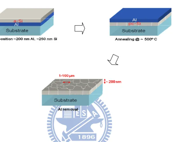
Fig. 2-3 shows schematically another alternative to make a pc-Si seed layer, this time via the AIC process.
(a) Al and a-Si deposition: As illustrated in Fig. 2-3 (a), an Aluminum (Al) layer of ~ 200 nm thick is evaporated on top of the substrate in a high vacuum e-gun evaporator. After the deposition, the Al layer is exposed to air for 2 minutes and results in a thin native oxide layer [19]. Like in the case of silicon the oxidation of aluminum is self-limited meaning that the oxide layer prevents further oxidation. After the thin oxide layer was formed, an a-Si layer (~ 200 nm thick) is evaporated on top of the Al in the same system.
(b) Annealing: The Al/a-Si layer stack is annealed for 5 hours in a tube furnace at 500°C in a nitrogen atmosphere. During the annealing, a layer-exchange takes place between the Al and the Si, and the a-Si crystallizes into pc-Si of large grains as illustrated in Fig. 2-3 (b). The oxide layer remains in the position throughout the annealing process by separating top and bottom layer during exchange phenomena and controls the diffusion process. The final results were a pc-Si layer with on top the aluminum layer.
(c) Al removal: After annealing, the Al layer is etched selectively by means of a chemical mixture containing phosphoric acid. Thus, the pc-Si seed layer on foreign substrate is obtained as shown in Fig. 2-3 (c) which can be used as seed layer for further epitaxial growth.
2.4 Epitaxial Growth
A stack of highly Boron doped p+ and a moderately Boron doped p-type pc-Si layer is epitaxially grown on the pc-Si seed layers. The growth mechanism involves thermal decomposition of a silicon precursor on the surface. CVD is possible over a wide range of temperature. The use of high temperatures results in a higher quality potential, but also a higher cost compared with low temperature techniques. Currently, the high temperature route was investigated for solar cell applications at IMEC. Heat-activated CVD system Epsilon2000 is used in this work. This is a Rapid Thermal Chemical Vapor Deposition (RTCVD) system.
The Epsilon2000 is a commercial thermal CVD system designed by ASM. The reactor works at atmospheric pressure and high temperatures (950-1250°C), deposition rates up to 10 mm / min is possible with very low defect density [21]. In this work, the deposition temperature was 1130°C with growth rate 1.4 um / min. Trichlorosilan (SiHCl3) diluted in hydrogen was used as precursor gas, the overall reaction can be
written as follows [22]:
SiHCl3+H2 Si+3HCl
sequences were typically grown on the seed layers a 0.5 μm layer with p+ doping of 3x1019 cm-3 followed by a 1.5 μm layer with p-type doping of 1016 cm-3. The thin p+
layer acts as a Back Surface Field (BSF) which Limits the recombination of minority carriers at the rear side and also provides a conductive path to the contacts for the collection of majority carriers. In the moderately doped layers, also called base, most of the photons are absorbed here and collected by the junction after converted into carriers. The growth process is consisted of several steps as flowing:
(1) Loading the sample at 250°C in N2 gas and heating up to 500°C. Draining and
introduction of H2 gas followed by rapid heating up to 1130°C in 92 seconds.
(2) Deposition of the p+ layer followed by a 10 to 30 second free step growth in H2 gas.
(3) The p layer deposition followed by cool down to 250°C under H2 gas.
Fine-grained pc-Si: Direct deposition of pc-Si on foreign substrate by CVD was also done in this work. Since the grain size is usually around 100 nm [23], the pc-Si done by direct deposition is regarded as fine-grained sample. This fine-grained pc-Si is prepared by direct sending substrates into exact the same epitaxial procedure as mentioned above but without forming a seed layer. The same oxidized Si substrate we used for seed layer formation is also used here for fine-grained pc-Si. A lot of nuclei are formed simultaneously during deposition, thus the resulting material has a very small grain size.
2.5 Solar Cell Fabrication
After the absorber layer was formed by epitaxial growth, a hydrogenation passivation step was introduced. The high density of defects at grain boundaries of poly-Si can be expected, especially the dangling bonds, which can trap carriers generated in the absorption layer. Enlarge the grain size of poly-Si may reduce such problem, but the fact is it cannot be unlimited enlarged. Therefore, together with enlarging the grain size, a defect passivition step is applied.
The passivation is carried out by direct plasma hydrogenation in PECVD system at a temperature of 400°C [23]. Just before loading, the samples are subjected to an HF (2%) dip to remove the native oxide. This oxide layer prevents the H-atoms to penetrate in the layer and might lead to a poor passivation. After loading of samples, the system is evacuated and the temperature is stabilized for about 10 minutes in flowing hydrogen. The plasma is ignited at 77 mW/cm2 and 2 Torr after which the power and the
pressure are immediately lowered to 62 mW/ cm2 and 1 Torr. The hydrogenation plasma temperature is around 400 °C at which the hydrogen ions are relatively mobile. To avoid out-diffusion of hydrogen during sample unloading, the layers are cooled down in the while the plasma kept switched on. After cooling down, the plasma is switched off and the samples are unloaded.
2.5.2 Emitter Formation
After the passivation step, an n-type emitter is formed. The emitter in the semiconductor solar cell can create an internal electric field in order to separate the minority carriers and majority carriers created after absorption of solar energy. Since our absorption layer is formed by p-type poly-Si, the emitter can be formed by creating an
n-type area. In this work a heterojucntion with intrinsic thin layer (HIT) emitter is used.
An intrinsic layer and an n+ a-Si layer were deposited by PECVD system in a raw. Just before loading, the samples get an HF dip (2%) to remove the native oxide and resulting in a hydrophobic pc-Si surface. After pumping down the chamber, its temperature is stabilized during 10 minutes. Then SiH4 (100 sccm) is introduced and the
gas flow is stabilized during another minute. After this conditioning of the chamber and the samples, the plasma is ignited at 37 mW/cm2, and the power is lowered to the deposition power which is in the range of 15 to 25 mW/cm2. When the intrinsic layer is deposited, the power is switched off and 100 sccm of diluted phosphine (1% PH3 in H2)
is added to the gas flow to deposit the n+ a-Si:H layer using the same plasma sequence as for the intrinsic a-Si:H layer. In order to give high absorption ability in emitter, the thickness was limited to only 15nm. Subsequently, 80 nm of Indium Tin Oxide (ITO) was deposited. This ITO serves as electrical conductor and also anti-reflection coating for the cell. The deposition of ITO was done at room temperature by RF sputtering.
In this work, the passivation was done before emitter forming in order to avoid crystallization or modification of the a-Si:H due to the temperature was around 400˚C while the a-Si:H deposition is done at temperature below 200˚C.
2.5.3 Contact Formation
As a final step, the n- and the p-type layer are contacted to extract current from and to apply a forward bias across the photovoltaic device. Since insulating substrates are used, both the emitter and the base contact are on the same side of the device (on top of
the silicon layer).
Two configurations can be used for the thin-film solar cells. In a superstrate configuration, the light enters the cell through the support onto which the active layer has been deposited. In a substrate configuration, the light penetrates through the other surface. Due to convenience at this stage of research, the pc-Si layers studied in this work have a substrate configuration with both contacts at the front side. Due to one-side contacting, the holes need to diffuse over a larger distance than in the conventional two-side contacted cells. Holes generated in the p-type layer need to travel vertically, down to the p+ layer, then horizontally towards the nearest contact and finally vertically to the contact itself. The horizontal distance determines the resistance and is the main contributor to the final series resistance of the cell. To limit losses in thin film polycrystalline solar cells, a careful design of the contact pattern is needed.
An interdigitated contact process is used in this work [23]. Here both emitter and base contacts consist of fingers and a busbar on top of the cell. Fig. 2-4 (a) shows the cross section schematic picture of interdigitated contact, and Fig. 2-4 (b) indicates the top view of a unit cell.
The generated electrons are collected through contact on emitter side as the white arrow shown in Fig. 2-4 (a). And the generated holes are collected through the base contact indicated by the black arrows in Fig. 2-4 (a). Since the actual vertical distance is only of few um, the resistance of the holes is mainly determined by the distance between two base contacts. This concept can also be used for larger cell areas and for thinner p+ layers. The base contacts are formed by lift-off photolithography and wet
chemical etching (HNO3/Buffer HF/H2O in volume ratios 40:1:16) of the n+ layer. After
fingers connected to a busbar, and the distance between two base contacts is around 1 mm. The holes thus need to travel over only 0.3 mm on average to reach the nearest contact.
After the evaporation of the base fingers, the front grid fingers were evaporated through a shadow mask in such a way that there are two emitter fingers around each base finger as can be seen in Fig. 2-4. The front grid fingers were made from a stack of Ti (70 nm), Pd (50 nm) and Ag (2μm). The Ti serves as a barrier for metal diffusion into the silicon, the Pd serves as adhesion layer between Ti and Ag, and the Ag contact is the conducting metal for the electrons. The spacing between two emitter fingers is also around 1 mm. In a last step the cells were separated by a second lithography process, where small areas of 1 cm2 are created after wet chemical etching. After etching, the final structure is annealed to ensure a good contact between metal contacts and silicon layer.
Chapter 3
Results and Discussion
3.1 Introduction
In this chapter, we will show the results of optimization and characterization of SPC seed layers. They will be discussed in different sections according to silicon deposition techniques and crystallization methods. We examine the crystallization results on our seed layers by several different methods, including X-ray diffraction (XRD), Transmission Electronic Microscope (TEM), Scanning Electron Microscope (SEM) and Optical Microscope. With these techniques it’s possible to determine the crystallization structure, crystalline fraction and grain properties, which is useful information for later correlation of the seed layer properties with the solar cell results. Resistivity versus temperature and Hall measurement are also carried out to determine the electrical properties in order to further optimum our pc-Si seed layer.
3.2 SPC Seed Layers Prepared by E-gun
Evaporation
3.2.1 P-type Doping Seed Layers
3.2.1.1 Crystallographic Properties
The annealing results for samples deposited by e-gun evaporation are listed in Table 3-1. These results are mainly based on X-ray diffraction examination. The thickness of pc-Si layer for examination here is around 480 nm, and we used Grazing Incidence XRD (GIXRD) mode to perform our measurement. The annealing summarize in Table 3-1 were carried out for 96 hours. As we can see from the Table 3-1, intrinsic a-Si deposited by electron beam evaporation cannot crystallize in 96 hours for annealing temperature lower than 600°C. On the other hand, the p-type a-Si layer starts to crystallize at the annealing temperature of 600°C. Both intrinsic and p-type a-Si were successfully crystallized at 650°C and 700°C.
Fig. 3-1 shows the X-ray diffraction graph of p-type samples annealing at 600°C (red line), 650°C (black line), and 700°C (green line) for 96 hours, and the blue line represents the as-deposited p-type a-Si layer. As we can see in the figure, the as-deposited layer has no peak in the 2θ range from 20° to 60°. Except the as-deposited layer, three typical peaks appear in the measured range for the annealed samples. These three peaks are located at 28.5°, 47° and 56° which represents the grain orientation of (111), (220), and (311) respectively.
However, the intensities of these peaks are different at different annealing temperatures. First, though the 600°C annealing sample has the peaks at the same detected angles as others, but its intensity is the smallest among them. As we increase
the annealing temperature from 600°C to 700°C, the intensity increases further. The intensity of X-ray diffraction graph can be regards as the amount of crystallization fraction [25]. The higher the intensity, the more fraction of the silicon film is crystallized.
A-Si has to gain enough energy to overcome the activation energy before transferring to pc-Si. Thus, there is an incubation time before crystallization happen during annealing process [26]. During this incubation time, no amorphous to crystal transfer happens but the a-Si keep absorbing thermal energy from the ambient. The incubation time related to the annealing temperature. When increasing the annealing temperature, the incubation time will decrease. This is due to higher annealing temperature provides more thermal energy, and thus it is more easily to transform into poly crystalline state. As a result, the crystallization fraction is higher when using higher annealing temperature for the same time. So we can see that 96 hours is not enough for the samples annealing at 600°C and 650°C. Thus the crystallization fraction is smaller and results in lower XRD intensity.
Besides the annealing temperature, control the annealing time may also let us see the progress of crystallization process. Fig. 3-2 shows X-ray diffraction graph of the boron doping sample annealing at 700°C for 24, 48, and 96 hours respectively. From the graph we can observe there is no peak when we only anneal for 24 hours, which can probably means that the crystallization process has not started yet. When we double the annealing time, the peak can be obviously observed from the graph. We further make the annealing time as long as 96 hours, and we can see the intensity of the peaks is further increased as expected. The very basic reason of time dependence phenomenon is actually the same as temperature dependence, the longer time you anneal the more
thermal energy you provide to the silicon layer. Thus the intensity will keep increasing and saturate when the whole layer is fully crystallized.
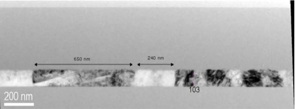
The TEM picture of Fig. 3-3 (a) shows a proof of not fully crystallized layer. The thickness of the as-deposited a-Si for examination was about 480nm, however, only 100nm ~ 110nm pc-Si were formed inside the whole silicon layer when annealing at 600°C for 96 hours, the other 375nm remained amorphous as we can see in the picture. As a result, the intensity of X-ray diffraction is much smaller (the red line in Fig. 3-1). Lots of planar defects are visible in boron doping e-gun deposited samples as illustrated in Fig. 3-3 (b).
From Fig. 3-4 (a), the TEM picture clearly shows that the whole a-Si layer of 480 nm was fully crystallized when annealing at 700°C for 96 hours. The surface was smooth and grains are cross the full layer thickness, which was what we want to further grow our epitaxial layer. Most grain sizes are several hundred nm but smaller than 1 μm. Lots of planar defects such as stacking faults are visible in boron doping e-gun deposited samples as illustrated in Fig. 3-4 (b). By comparing TEM pictures of Fig. 3-3 and Fig. 3-4 we can observe the crystallization process occurred heterogeneously from the interface of SiO2 and a-Si rather than homogeneously inside the whole a-Si layer.
The crystallization preferentially start from the interface was observed ordinarily in previous works [27]-[29].This phenomenon is believed due to the release of stress induced by the thermal expansion difference between Si and SiO2 [29]. In Fig. 3-3, the
surface of pc-Si shows rather rougher than those fully crystallized surface of pc-Si as in Fig. 3-4 is probably due to the crystallization process was not finished yet.
3.2.1.2 Electrical Properties
The electrical activation of the defects at the grain boundaries is studied by measuring the resistivity ρ of majority carriers in seed layers as a function of temperature (300 – 500°K) (Fig. 3-5). Here, three samples annealing at 600°C, 650°C, and 700°C for 96 hours are measured. The ρ vs. T measurements are carried out in a four point probe configuration (HP4156) with sintered Al patterns as contacts. The curves show a decrease of the resistivity with increasing temperature. Normally on mono-crystalline silicon, an increase of the resistivity is found with increasing temperature due to an enhanced phonon scattering. For pc-Si the situation is different. Here, the resistivity of the pc-Si layers is the sum of the intra-grain resistivity and the resistivity of the grain boundaries, which is usually much larger and determines the total resistivity [30]. At a higher temperature more carriers can surmount the potential barrier (a higher thermionic current) and a lower resistivity is observed.
As can be seen in Fig. 3-5, increasing the annealing temperature lowers the resistivity with slopes are almost the same to each other. The slopes in the graph are related to the activation energy and could be further calculate by Setto’s [30] model to estimate the carrier trapping density at the grain boundary if the doping concentration is known. Probably the potential barrier at the grain boundaries are similar for all measured samples and independent of annealing temperature because it can be assumed that the activation energy is linked to the potential barrier. The resistivity decreases with increasing annealing temperature might caused by intra-grain resistivity and different crystallization fraction as concluded from X-ray graphs.
3.2.2 Intrinsic Seed Layers
3.2.2.1 Crystallographic Properties
X-ray diffraction graph of intrinsic Si isothermal annealed at 600°C, 650°C, and 700°C for 96 hours are shown in Fig. 3-6. The thickness of the layer is also around 480 nm. Same trend as p-type samples can be observed here, increasing the annealing temperature will also increase the intensity of each peaks. Contrary to the p-type layers, annealing at 600ºC for 96 hours was not sufficient for intrinsic a-Si layers deposited by e-gun evaporation. To investigate if the crystallization is impossible or not, one extra annealing was done for 173 hours. XRD measurement showed that only the samples annealed at 173 hours started to show the typical peaks as indicated in Fig. 3-7.
According to Van Vecheten et al. [31], the number of charged vacancies increases when the Fermi level moves up or down from the mid-gap position. As dangling bonds are more common defects than vacancies in a-Si, these dangling bonds may play a similar role in the crystallization mechanism. As mentioned in chapter 2, the dangling bonds at the interface of amorphous to crystalline silicon actually are only certain sites available for crystallization [32]. These dangling bonds diffuse from the bulk towards the amorphous to crystalline interface during annealing and the capture cross section at the interface depends on the charge state of the dangling bonds and modifies the crystallization process. The change of their charge states is responsible of the enhancement of crystallization process due to electrical activity [32].
Besides the dependence on temperature, Fig. 3-8 shows the dependence on annealing time for intrinsic samples. Like p-type doping samples, there is no crystallization can be observed after annealing for 24 hours, but after 48 hours annealing we can clearly see the three peaks which means it started to crystallize.
3.2.2.2 Electrical Properties
The ρ vs. T measurements was also done on intrinsic e-gun seed layers and are shown in Fig. 3-9. The difference of slopes between p-type (blue lines) and intrinsic (red lines) samples can be observed in Fig. 3-9. The slope is larger for intrinsic samples due to higher activation energy. Though we do not really know the doping level of our p-type sample, but we can see that the doping samples have lower resistivity which means they are in the second regime of Setto’s model [30]. This means that the doping concentration is at least more than the trapping density at the grain boundaries. Due to the high resistivity at room temperature, Hall effect measure was not possible to carry out on both types of samples.
3.3 SPC Seed Layers Prepared by PECVD
Samples prepared by PECVD method annealing at 600°C are listed in Table 3-2, the annealing time was as long as 96 hours. As mentioned in chapter 3, because of the n+ a-Si deposited at 300°C blistered right after deposition, we had no further
investigation on it. Also due to the main purpose in this work is comparing SPC seed layers with AIC seed layers, which is heavily doped p-type pc-Si. Thus, we had more focus on p-type doping silicon.
Besides the three crystallized samples in Table 3-2, we can observe peeling off phenomenon happened after annealing. There were two samples, namely n-type and p-type doping ones deposited at 200°C, peeled off at 600°C. As we increased our annealing temperature, this phenomenon becomes more and more serious. All the samples annealing at 650°C and 700°C peeled off. Fig. 3-10 shows the pictures of the
peeling off samples. As can be observed, the surface was totally damaged and no further investigation is possible to be done on such layer. This peeling off phenomenon may probably caused by the H2 component exists inside the silicon film as we used H2 as
dilute gas in the deposition process.
3.3.1 Crystallographic Properties
Fig. 3-11 shows the X-ray diffraction graphs of the three successfully crystallized samples. Three clearly peaks at 28.5°, 47°, 56°, are shown in each of them. And the peaks shown at these angles represent grain orientations of (111), (220), and (311) respectively, which are exactly the same as samples deposited by e-gun. The peak intensities are almost the same in each of them, which can be regarded as they all have the same crystallization fraction. In order to examine the crystallization fraction, we had the TEM picture. By TEM picture (Fig. 3-12) taken from the intrinsic sample deposited at 200°C and annealed at 600ºC for 96 hours we can see the whole a-Si layer was converted into pc-Si. And thus we can conclude that all the three samples are fully crystallized. From the picture we can also see that the surface of pc-Si layer is smooth and most grains are cross the full layer thickness, which is what we want to further grow our epitaxial layer. Most grain sizes are several hundred nm and smaller than 1 μm. As indicated in the Fig. 3-12 (a) by an arrow, there is one clear grain with the grain size about 1000 nm. Lots of planar defects are also visible in these grains as indicated in Fig. 3-12 (b).
Fig. 3-13 shows the intrinsic PECVD a-Si deposited at 200°C after annealing at 600°C for several different time periods. As can be seen in the graph, there is no peak
can be observed after annealing for 12 hours. But after annealing for 24 hours, the crystallization process started, thus we can see the peaks with very small intensity. The peak intensity keep increasing with annealing time and saturated when the whole layer was fully crystallized, which is around 96 hours as can be seen from the graph. Fig. 3-14 and Fig. 3-15 show the X-ray diffraction graph of intrinsic a-Si deposited at 300°C and boron doped a-Si deposited at 300°C respectively. Comparing to Fig. 3-13, there is nothing very different can be observed between each other even between doping and without doping. We only choose four different annealing times to compare the differences between each of them. Of course it is possible to see more detail into the crystallization progress if the time interval is smaller or using in-situ XRD versus time [33].
3.3.2 Electrical Properties
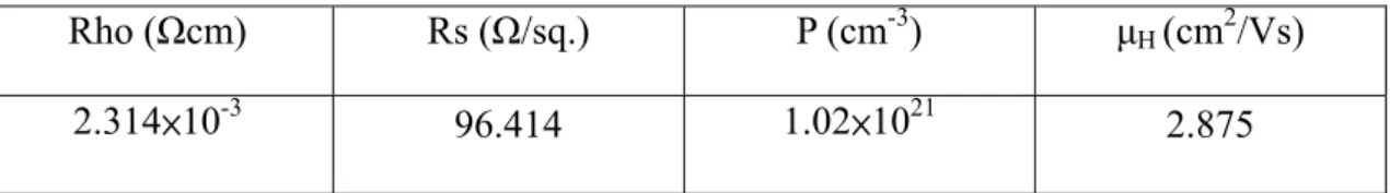
The ρ vs. T measurement is also carried for PECVD samples and shown in Fig. 3-16. The two intrinsic samples both have high resistivity at room temperature, which are around 4 105 to 5 105 Ωcm with slopes very close to each other. These values are almost the same as intrinsic e-gun samples as shown in Fig. 3-17. From these measurements we may conclude that if the grain sizes of these intrinsic samples are in the same range, then their trapping densities at the grain boundaries could be at the same order of magnitude.
There is an obvious drop of resistivity for the p+ PECVD sample (green line in Fig. 3-9). The resistivity is at the order of 10-3Ωcm at room temperature. The dramatically drop of resistivity is probably caused by high concentration of dopants compensated all