國
立
交
通
大
學
電子工程學系 電子研究所
博 士 論 文
快閃式記憶體和金氧半電晶體元件中單一電荷
所導致的可靠性議題研究
Single Charge Phenomena in Scaled Memory and
CMOS Devices
研 究 生:馬煥淇
快閃式記憶體和金氧半電晶體元件中單一電荷
所導致的可靠性議題研究
Single Charge Phenomenon in Scaled Memory and
CMOS Devices
研 究 生:馬煥淇 Student:Huan-Chi Ma
指導教授:汪大暉 Advisor:Tahui Wang
國 立 交 通 大 學
電子工程學系 電子研究所
博 士 論 文
A DissertationSubmitted to Department of Electronics Engineering and Institute of Electronics
College of Electrical and Computer Engineering National Chiao Tung University
in partial Fulfillment of the Requirements for the Degree of
Doctor of Philosophy in
Electronics Engineering January 2011
快閃式記憶體和金氧半電晶體元件中單一電荷
所導致的可靠性議題研究
學生:馬煥淇
指導教授:汪大暉
博士
國立交通大學
電子工程學系 電子研究所
摘
要
本篇論文主要探討在以氮化矽(SiN)為電荷儲存之快閃式記憶元件以及高介 電閘極材料(high-k)金氧半電晶體元件中,單一電荷引致的可靠性議題研究。隨 著高介電閘極的採用,其元件在加壓後的電流不穩定狀態之研究的重要性也逐漸 增加。另外,隨著元件不斷地微縮,數顆載子散逸流失以及隨機電報雜訊(RTN) 對於通道電流會造成顯著的影響,而隨機電報雜訊對浮動閘極快閃式元件操作的 影響近來已廣泛地被討論,但是,隨機電報雜訊對於氮化矽快閃記憶體操作的影 響只有少數論文提及,因此,本論文前半段的研究著重於氮化矽快閃記憶體中的 隨機電報雜訊,在氮化矽快閃記憶體元件中,吾人基於隨機電報雜訊開發新穎一 種方法來分析注入電荷的分布,並且深入討論隨機電報雜訊於浮動閘極與氮化矽 快閃記憶體元件操作的不同影響之原因,接著,討論氧化鉿量子點快閃記憶體電 荷流失機制,而本論文後半段,提出雙極電荷散逸模型來解釋在高介電閘極電晶 體施加電壓溫度後所引致的電流轉彎實驗現象。 第一章中,說明隨著元件不斷微縮,單一載子北補捉/釋放所造成的隨機電 報雜訊及少數載子散逸流失現象對元件通道電流會造成顯著的影響,並且對於隨機電報雜訊對於浮動閘極快閃記憶體操作之可靠性議題快速地回顧,另外,亦對 量子點快閃記憶體材料作一精簡回顧。
第二章中,吾人研發一新穎方法來偵測小面積SONOS 快閃記憶體沿著通道 的表面電位變化,這個新方法是藉由結合缺陷位置萃取技術和底層二氧化矽缺陷 所產生的隨機電報雜訊(Random Telegraph Noise)來達成。吾人使用這個新方法 來驗證 SONOS 快閃記憶體中通道熱電子(Channel Hot Electron)的寫入電荷分 佈和通道引發二次電子射入的電荷分佈之不同。此外,這個方法也被應用在觀察 通道熱電子寫入和能帶到能帶穿隧產生之熱電洞(Band-to-Band Tunneling Hot Hole)抹除電荷分佈的不對稱現象。最後,亦利用此方法研究對於氮化矽記憶元 件資料流失的機制,而我們藉由量測在寫入電子流失時電流的變化,推論出寫入 電子是經由垂直方向經由底部氧化層穿遂流失。
在第三章中,我們研究了氮化矽快閃式記憶體(SONOS Flash Memory)中的 寫入載子對隨機電報雜訊(Random Telegraph Noise)之振幅的影響。同時,我們 對浮動閘極快閃式記憶體(Floating Gate Flash Memory)、氮化矽快閃式記憶體做 了測量與模擬的工作。我們發現氮化矽記憶元件在資料寫入後隨機電報雜訊振幅 分布與寫入前不同,而浮動閘極記憶元件在資料寫入前後有相同的隨機電報雜訊 振幅。兩者的不同歸因於在氮化矽快閃記憶體中,隨機且分離的寫入載子造成的 電流路徑滲透作用。 第四章探討高介電材料量子點快閃記憶體元件資料流失的機制。吾人分別在 不同溫度下量測資料流失速度。相較於氮化矽快閃記憶體元件,高介電材料量子 點快閃記憶體元件資料流失速度有強烈的溫度正相關性,無法以是適於氮化矽快 閃記憶體的 Frenkel-Poole 激發理論解釋。吾人提出一種新的電荷流失機制:藉 由熱激發穿隧機制,成功解釋其電荷流失的強烈溫度關係。
第五章中,研究高介電閘極(HfSiON) pMOSFETs 在施加負電壓溫度後所導 致的不穩定現象,以單電子散逸量測技術針對施加負電壓大小、量測電壓大小及 施加溫度作仔細的討論,在某特定條件下,加壓後電流將從退化變化為增益模 式,吾人提出雙極電荷散逸模型來解釋負電壓溫度加壓所致之汲極電流的此轉彎 (turn around)現象。其原因為在不同的施加電壓溫度及量測電壓下,加壓電流的 電洞與電子成分不相同所致。 最後於第六章,吾人將對本論文做個總結。 關鍵字: 隨機電報雜訊,先進互補式金氧半電晶體,氮化矽快閃式記憶元件,浮 動閘極快閃記憶體,負電壓溫度引致不穩定,高介電閘極氧化層,單電 荷散逸,雙極電荷散逸模型,橫向電荷分佈,垂直電荷流失機制,橫向 電荷流失機制,熱電子注入,熱電洞注入,滲透路徑,不均勻通道電位 分佈
Single Charge Phenomena in Scaled Memory
and CMOS Devices
Student: Huan-Chi Ma Advisor: Dr. Tahui Wang
Department of Electronics Engineering & Institute of Electronics
National Chiao Tung University
ABSTRACT
This thesis will focus on the reliability issues of single charge phenomenon in nonvolatile flash memory device and advanced gate dielectrics CMOS device. A novel technique based on random telegraph signal (RTS) is proposed to characterize the program/erase charge profile and retention in SONOS device. Besides, the different program charge effect between floating gate (FG) and SONOS flash device is investigated. Furthermore, staircase-like post- negative bias temperature (NBT) current instability is investigated by a computer-automated measurement circuit, which minimizes the switching delay between stress and measurement.
In Chapter 1, single electron induced current fluctuation in sub-micron FETs will be introduced. First, trapping and detrapping of individual oxide defects has been readily measured in CMOS device and nonvolatile memory. Second, the phenomena of drain current steps due to individual defects in NBTI relaxation
transients will be described. Also, the impact of single charge induced current variation will be pointed out. The application of nano-crystals in nonvolatile memory will be made a short introduction.
In Chapter 2, a new RTS-based method is proposed to characterize the lateral distribution of injected charge in program and erase states in a NOR-type SONOS flash memory. The concept of this method is to use RTS to extract an interface trap position in the channel and then to use the interface trap and RTS as internal probe to detect a local channel potential change resulting from injected charge during program/erase. The lateral width of the injected charge induced channel potential barrier is shown to be around 20nm in channel hot electron (CHE) program by this method. We also find that channel initiated secondary electron (CHISEL) program has a broader injected charge distribution than CHE program. A mismatch of CHE program electrons and band-to-band tunneling erase holes is observed. The polarity of a program-state charge distribution is examined along the channel within 10-20 program/erase cycles. Nitride charge retention loss is observed by using this method.
To expound the different program charge effect between FG flash and SONOS flash, in Chapter 3, RTN in planar SONOS cells and floating-gate cells in erase state and program state are measured, respectively. We find that a SONOS cell has a wide spread in RTN amplitudes after programming while a floating gate cell has identical RTN amplitudes in erase and program states at the same read current level. A 3D atomistic simulation is performed to calculate RTN amplitudes. Our result shows that the wide spread of program-state RTN amplitudes in a SONOS cell is attributed to a current-path percolation effect caused by random discrete nitride charges.
In Chapter 4, the charge retention loss mechanism in a hafnium oxide (HfO2) dielectric dot flash memory is investigated. The temperature and time dependence of a charge loss induced gate leakage current in a large area cell are measured directly. We find that the charge loss is through a top oxide in the cell and the stored charge emission process exhibits an Arrhenius relationship with temperature, as opposed to linear temperature dependence in a SONOS flash memory. A thermally activated tunneling front model is proposed to account for the charge loss behavior in a HfO2 dot flash memory.
In Chapter 5, bipolar charge detrapping induced current instability in HfSiON gate dielectric pMOSFETs after negative bias and temperature stress is studied by using a fast transient measurement technique. Both single electron and single hole emissions are observed, leading to post-stress current degradation and recovery, respectively. The NBT stress voltage and temperature effect on post-stress current evolution is explored. Clear evidence of electron and hole trapping in NBT stress is demonstrated. A bipolar charge trapping/detrapping model and charge detrapping paths based on measured charge emission times are proposed. Finally, conclusions are made in Chapter 6.
Keywords: Random Telegraph Signal, SONOS, Floating-gate Flash, NBTI, high-k dielectric, Single charge emission, Bipolar charge detrapping model, Lateral charge distribution, Lateral charge loss mechanism, Vertical charge loss mechanism, Hot electron programming, Percolation path, non-uniform channel potential
ACKNOWLEDGEMENT
First of all, I would like to express my deepest gratitude to my
advisor Prof. Tahui Wang for his continuous guidance and
encouragement. Without his teaching, I cannot complete my
dissertation.
I also show my appreciation to all of my committee for their
suggestions and comments.
During my study, many important persons have influenced
me. Mr. S. H. Ku, Mr. C. T. Chan and J. W. Wu have taught me a
lot of invaluable knowledge; special thanks are given to Mr. C. J.
Tang and Mr. C. C. Cheng for sharing experience together. In
particular, the assistance in measurement from Mr. C. H. Lee, Mr.
Y. P. Chao, Mr. Y. L. Chou, Mr. J. P. Chiu, Mr. T. Y. Lin, Mr. Y. T.
Chung and Mr. C. W. Lee are also greatly appreciated. I am also
indebted to the Wang and Chung group members of Emerging
Device and Technology Lab, who had made life fun.
Finally, I would present the deepest love to my parents. Their
love is the most important power supporting me. This dissertation
is dedicated to them.
謝誌
首先,這本博士論文的完成,必須感謝我的指導老師汪大暉教
授。他有深厚的理論基礎,再加上細心與耐心的指導態度,使得我很
容易從他的隻字片語中學習到新的知識及觀念。從討論中吸取汪老師
的思考模式及獨到的見解,已成為我學習獨立思考的不二法門。
在論文的研究上必須感謝許多曾經指導過我的許多學長
,及一起
參與研究的同學及學弟。首先感謝古紹泓及詹前泰學長在我剛進研究
生活的指導與鼓勵;感謝鄭志昌學長及唐俊榮同學在研究領域上的協
助及討論
。同時,我也感謝在李智雄學弟,趙元鵬學弟,周佑亮學弟,
邱榮標學弟,林東陽學弟及鐘岳庭學弟在實驗執行上的幫助
。此外,
感謝許智維同學,李冠成學弟,薛至宸學弟,吳致融學弟,許家源學
弟,林彥君學妹,李致維學弟以及前瞻元件與技術實驗室所有成員,
他們為我的博士生涯增色許多。
最後,我要感謝我的父母、家人及女友小儀,在攻讀博士班期間
給我的鼓勵與支持,有他們在背後無怨無悔的付出與關心,讓我毫無
顧忌的專注於論文研究,使得這本博士論文得以順利完成。這本論
文,獻給他們。
Contents
Chinese Abstract
iEnglish Abstract
ivAcknowledgement
iixContents
xFigure Captions
xiiiTable Captions
xixList of Symbols
xxChapter 1
Introduction
11.1 Background 1
1.2 Description of the Problem 2 1.3 Organization of the Dissertation 4
Chapter 2
A Novel Random Telegraph Signal Method to
Study Program/Erase Charge Lateral Spread and
Retention Loss in a SONOS Flash Memory
92.1 Preface 9
2.2 Device Description and Measurement Setup 12 2.3 Measurement Result and Discussion 12
2.3.1 Extraction of an Interface Trap Position 12 2.3.2 CHE Program Charge Lateral Profile 14
2.3.3 CHE versus CHISEL programming 15 2.3.4 CHE Program/BTBT Erase Charge Mismatch 15 2.3.5 Program Charge Retention Loss 16
Chapter 3
Program Charge Effect on Random Telegraph
Noise Amplitude in Floating Gate and SONOS
Flash Memory
403.1 Preface 41
3.2 Device Description and Measurement Setup 41
3.3 Results and Discussions 41
3.3.1 Comparison of the Erase- and Program-state RTN in a
FG and SONOS Cell 41
3.3.2 Statistics Results of Erase-state and Program-state in FG
and SONOS devices 42
3.3.3 3D Atomistic Simulation of RTN 43
3.4 Summary 44
Chapter 4
Charge Retention Loss in a HfO
2Dot Flash
Memory via Thermally Assisted Tunneling
554.1 Preface 55
4.2 Device Description and Measurement Setup 56
4.3 Results and Discussions 56
4.3.1 Gate Leakage in HfO2 dots memory and SONOS 56 4.3.2 Thermally Activated Tunneling Front Model 57
4.4 Summary 57
Chapter
5
Study of Post-NBT Stress Current Instability
Modes in HfSiON Gate Dielectric pMOSFETs by
Measurement of Individual Trapped Charge
Emissions
645.1 Preface 64
5.3.1 Evidence of Holes and Electrons Detrapping in
Post-NBT Stress Current 65
5.3.2 Stress Vg and temperature effect on Post-NBT Current
Instability 66 5.3.3 Measurement Vg Dependence on Post-NBT Current
Instability 67 5.3.4 Bipolar Charge Detrapping Model 68
5.4 Summary 68
Chapter 6
Conclusions
80References
82Vita
96FIGURE CAPTIONS
Chapter 1
Fig. 1.1 A typical step-like “quantum jump” observed in channel current during NBTI recovery in a SiO2 pMOSFET.
Fig. 1.2 A two-level RTS waveform resulting from electron emission and capture at oxide trap. τc and τe are electron emission time and capture time. ΔId is RTS amplitude.
Fig. 1.3 Estimation of threshold voltage shift as a function of process node [1.30] Fig. 1.4 (a) Noise distributions of 90nm, 70nm, 50nm flash memory technologies [1.31]
and (b) Measured Vth distribution of a 4-level MLC with level enlarged [1.30].
Chapter 2
Fig. 2.1 Illustration of a two-level RTS waveform resulting from electron emission and capture at an interface trap. c and e are electron emission time and capture time. The trap position is xt from the drain junction. The channel potential right below the trap is denoted by Vts.
Fig. 2.2 Gate voltage dependence of average capture time in RTS at two drain voltages, Vds=0.05V and 0.3V. The lateral shift of these two curves corresponds to ΔVts.
Fig. 2.3 Cumulative trap position distribution along the channel. L=0.1μm is the channel length and xt is the distance of a trap from the drain.
Fig. 2.4 RTS patterns at three program ΔVt=0.3V, 0.9V and 1.2V in a CHE program cell. The RTS measurement condition is Vgs=3.5V and Vds=0.05V. xt =0.2L. Fig. 2.5 Average capture time (τc) and emission time (τe) versus program ΔVt in an xt
=0.2L cell. 5 6 7 8 21 22 23 24 25
Fig. 2.6 Ratio <τc>/<τe> and a local surface potential change (Δϕs) at the trap position (xt =0.2L) versus program ΔVt. The local potential change is calculated from Eq. (2).
Fig. 2.7 Evolutions of <τc>/<τe> with program ΔVt at four different trap positions xt=0.03L, 0.05L, 0.2L and 0.3L.
Fig. 2.8 Channel potential energy distribution extracted from RTS. The CHE program window is ΔVt=0.6V. The width of the potential energy barrier is about 20nm. Fig. 2.9 Comparison of <τc>/<τe> evolutions with program ΔVt in CHE and CHISEL
program. A substrate bias of -2V is applied in CHISEL program.
Fig. 2.10 <τc>/<τe> versus program ΔVt during CHE program and BTBT hot hole erase. The device has a trap at 0.05L from the drain. The inset shows the <τc>/<τe> in a log scale.
Fig. 2.11 <τc>/<τe> versus program ΔVt during CHE program and BTBT hot hole erase. The device has a trap at 0.3L from the drain.
Fig. 2.12 Illustration of program/erase charge distributions in the channel. The stars represent interface traps. The program electrons at xt=0.05L are completely compensated, but some far electron at xt=0.3L are not compensated by erase holes.
Fig. 2.13 <τc>/<τe> in a program-only cell versus bake time. The xt is 0.03L. The bake temperature is 120℃. The program ΔVt is 1V.
Fig. 2.14 Program-state and erase-state <τc>/<τe> at different P/E cycles. The xt is 0.05L. The <τc>/<τe> in fresh state is also shown in the figure. The program ΔVt is 1V.
Fig. 2.15 Program-state <τc>/<τe> is plotted against gate stress time. The program ΔVt is 1V. The gate stress voltage is Vg=-5V. The trap position xt is 0.05L. RTS waveforms immediately after program and after 4-second gate stress are shown in the inset of the figure.
26 27 28 29 30 31 32 33 34 35
Fig. 2.16 (a) Read current variation with cumulative gate stress time in program state. The P/E cycle number is 33. (b) Experimental setup for read current measurement. The measurement consists of two alternating phases, a gate stress phase and a read phase. In gate stress, a negative gate voltage (-3.5V) is applied to accelerate nitride charge loss. The sampling rate is 10kHz. The program ΔVt is 2V.
Fig. 2.17 Step-like drain current during retention time in a SONOS NAND cell with uniform FN program/erase.
Chapter 3
Fig. 3.1 An illustration of random potential induced percolation effect (fromRTN [3.7]) in FG cell.
Fig. 3.2 RTN amplitude versus drain current in a FG flash cell in three P/E cycles. The Vt window is 1V. The drain voltage in measurement is 0.7V and the gate voltage is varied.
Fig. 3.3 RTN amplitude versus drain current in a SONOS cell in three P/E cycles. The Vt window is 1V. The drain voltage in measurement is 0.7V and the gate voltage is varied.
Fig. 3.4 Measured RTN waveform and Id versus Vg plot (a) in erase-state and (b) in program-state of a SONOS cell. Electron trapping at an interface trap is manifested by a current discontinuity in the Id-Vg plot
Fig. 3.5 An illustration of two different program charge storage characteristic resulting distinct outcome of percolation path. Continuous distribution in FG flash and random discrete distribution in SONOS flash.
Fig. 3.6 Measured program-state RTN amplitude versus erase-state RTN amplitude in 40 FG flash cells. The RTN amplitude is measured at Id=500nA @Vd=0.7V. The device dimension is W/L=0.11μm/0.09μm. The program window is 1V or 2V. 36 38 46 47 48 49 45 50
Fig. 3.7 Measured program-state RTN amplitude versus erase-state RTN amplitude in 45 planar SONOS cells. The RTN amplitude is measured at Id=500nA @Vd=0.7V. The SONOS cells have W/L=0.09μm /0.08μm, a 2.8nm tunnel oxide, a 6nm SiN and a 6nm top oxide.
Fig. 3.8 Simulation flowchart of 3D atomistic simulation for RTN amplitude at program state and erase state for FG and SONOS flash.
Fig. 3.9 Simulated RTN amplitude versus drain current in a FG flash cell. Program-state and erase-state have the same placement of substrate random dopants. The RTN trap is placed in the middle of the device.
Fig. 3.10 Simulated RTN amplitude versus drain current in a planar SONOS cell. Program-state and erase-state have a fixed placement of substrate dopants. Ten different sets of random program charges are simulated. An RTN amplitude due to number fluctuation is calculated with continuous substrate doping and program charges.
Chapter 4
Fig. 4.1 Measured gate leakage current at Vg=0V versus time in a HfO2 dot flash memory cell (500μm×500μm). The temperature is from 25℃ to 125℃. The device is programmed to a threshold window of 3V.
Fig. 4.2 Comparison of temperature dependence of a gate leakage current in a HfO2 dot flash and in a SONOS flash at t=3s.
Fig. 4.3 Arrhenius plot of the gate leakage current in a HfO2 dot flash memory. The retention time is 0.5s and 5s. The extracted activation energy is 0.19eV.
Fig. 4.4 (a) Illustration of charge loss through a top oxide trap in a HfO2 dot flash. (b) Energy band diagram and thermally assisted tunneling of a trapped charge.
51 52 53 54 60 61 62 63
Fig. 5.1 Voltage waveforms applied to the gate and the drain during NBT stress and measurement (relaxation) phases. A high-speed electronic switch is used to minimize a delay between stress and measurement.
Fig. 5.2 Post-stress current evolution with measurement (relaxation) time in (a) a small area device (W/L=0.18/0.08μm) and (b) a large area device (W/L=10/0.32μm). The NBT stress voltage is -3.0V. The measurement voltages are Vg/Vd=-1.2V/-0.2V and temperature is 25°C. The pre-stress current is shown in (a) for comparison. Both current degradation and recovery are obtained in the measurement period.
Fig. 5.3 Linear drain current change versus NBT stress time. ΔId is measured immediately after stress. Three stress voltages, Vg =-2.8V, -2.6V and -2.0V are applied. Electron trapping into pre-existing high-k traps is demonstrated by a positive ΔId at a high stress |Vg|.
Fig. 5.4 Drain current evolution after a low Vg (=-2V) stress in (a) a small area device and (b) a large area device. Only hole detrapping are found at a low stress Vg. The measurement voltages are Vg/Vd=-1.2V/-0.2V and temperature is 25°C. Fig. 5.5 Illustration of a band diagram and carrier flows in a high-k pMOSFET under
-Vg stressing. In a charge separation measurement, the electron stress current (Ie) flows from the substrate to the gate and the hole stress current (Ih) flows from the source/drain to the gate.
Fig. 5.6 Stress voltage dependence of electron injection current (Ie) and hole injection current (Ih). A charge separation technique is used to measure Ie and Ih. (a) T= 25°C and (b) T= 100°C.
Fig. 5.7 Post-stress current evolutions with measurement time for two different stress temperatures, T= 25°C and 80°C. The stress voltage is -2.2V. The turn-around characteristic is observed only at T= 80°C. Note that the Id measurement is
69 70 71 73 72 74
Fig. 5.8 Typical post-stress current evolution patterns. (a) measurement Vg=-0.85V and (b) Vg=-1.0V. The longest electron detrapping time (τe) and the shortest hole detrapping time (τh) are indicated. The trend is that both τe and τh increase with measurement |Vg|.
Fig. 5.9 Average τe and τh are plotted against measurement Vg. We repeated measurement of each data point ten times by charge re-filling to take an average. Only the longest electron detrapping time and the shortest hole detrapping time (as shown in Fig. 8) are plotted in the figure.
Fig. 5.10 Illustration of the energy band diagram in relaxation phase. (a) Trapped electron emission to the gate, and (b) trapped hole emission to the substrate. Fig. 5.11 Arrhenius plot of the τe and τh versus temperature (a) trapped electrons and
(b) trapped holes. The extracted activation energy is 0.2eV for electrons and 0.14eV for holes.
76
77
78
Table Captions
Table 2.1 Dependence of program-state Vt retention loss on retention time, P/E cycles, gate stress polarity and temperature from the vertical charge loss model (in a FP emission limited condition) and from experimental results. 39
LIST OF SYMBOLS
Ea Activation energy
ET Trap energy
EF Fermi level
F Electrical field in nitride Ie Electron stress current
Ih Hole stress current
Id Drain current
L Channel length
me Electron effective mass in SiO2
N P/E cycle number
Nox Oxide trap density Nt Trap density in top oxide
ne Electron concentration in the channel right below the trap nt Trapped charge density in silicon nitride
Qs Stored charge in the HfO2 dot
Qox Negative trapped charge in the bottom oxide
T Absolute temperature
t Measurement time
tox The oxide thickness
Vt Threshold voltage
Vg, Vd, Vs Gate, drain, and source voltage Vts Channel potential at the trap position
W Channel width
xt Distance of the trap from drain edge
αox Coefficient of tunneling probability through SiO2
ΔId RTN amplitude
ΔVt Program window
Δφs Local potential change at the trap position εox Dielectric constant of SiO2
φb Barrier height between the SiO2 and Si3N4 for electrons σ RTN amplitude distribution standard deviation σt Trap cross section
τe, τc Electron emission time and capture time
τe(FP), τc(FP) Frenkel-Poole emission time and capture times
τeff Effective time for nitride trapped charge at the
emission front to escape from the ONO film τox Oxide tunneling time
υth Thermal velocity
Chapter 1
Introduction
1.1 Backgrounds
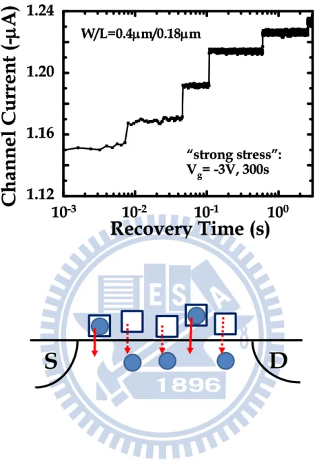
In order to maintain the scaling roadmap, high permittivity (high-k) material is introduced to replace SiO2 to solve the gate leakage problem. Bias temperature stress induced current instability in SiO2 and high-k based gate dielectric CMOS was reported to be mainly issue on DC performance [1.1]-[1.8]. With the shrinkage of device dimension to atomic levels, variation between devices occurred due to the effects such as random dopant fluctuation [1.9]-[1.15]. Similarly, the effect of a single charge induced current fluctuation on a typical device can be quite significant.. In ultra small area device, the trapping of even a single carrier will potentially cause functional errors in digital logic circuits and memories. The effect of few carriers trapping has also become a major reliability issue in bulk MOSFETs. MOSFET degradation associated to trapping of carriers in stress-generated defects in the gate dielectric has become a matter of growing concern [1.16]-[1-21]. Fig. 1.1 illustrates multiple carriers were detrapping in negative bias stressed device [1-22]
Flash memory is a non-volatile computer data storage technology that can be electrically programmed, erased and read for many times and won’t be lost after cutting off the power. It is primarily used in memory cards, USB flash drives, and solid-state drives for general storage and transfer of data between computers and other digital products. With respect to charge storage devices, two state-of-art techniques attract great attention. (a) Floating gate (FG) devices: charge is stored in a thin conducting or semiconductor layer. (b) Charge trapping devices: Charge is stored in the traps at the interface and bulk of insulator, such as SONOS
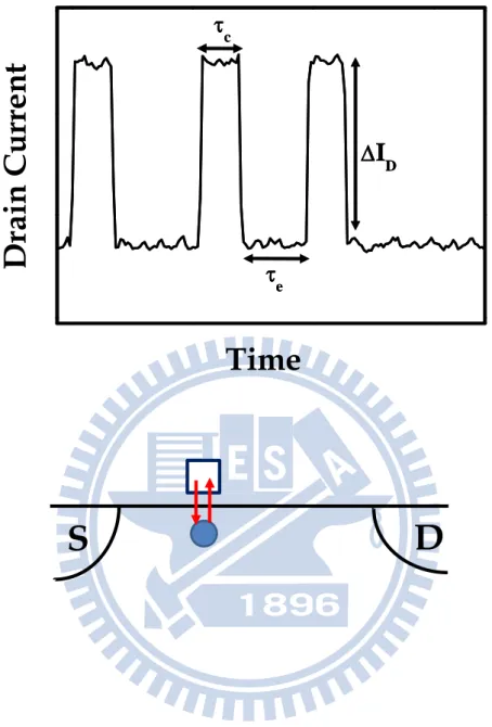
device [1.23]. With the advanced VLSI processing, the effect of a single electron on a typical device can be quite significant. Such effects will eventually cause fundamental scaling and reliability problems. Random telegraph noise (RTN) phenomenon arising from electron emission and capture at an interface trap site [1.24]-[1.27] has been recognized as a new scaling concern in flash memory [1-28]-[1-33]. Typical two-level RTN pattern is shown in Fig. 1.2. Vt fluctuations originated from a large-amplitude RTN tail will cause a read error and become a prominent issue in designing a multilevel-cell (MLC) flash memory in 45nm technology node and beyond as shown in Fig. 1.3[1-30]. Fig. 1.4(a) shows that the worst case of RTN induced Vt shift is over 0.3V in 50 nanometer technology node [1-31]. Fig. 1.4(b) tells us that such large RTN tail may cause a read error in multilevel-cell flash memory application and requires the use of error code correction.
Another category of discrete charge storage flash memories are to use nano-crystals as storage nodes. Many different types of nano-crystals from semiconductors (Si, Ge) to metals (W, Au) have been proposed [1-34], [1-35]. Recently, a HfO2 dielectric dot flash memory with hot electron program/hot hole erase was presented with superior characteristics in terms of a large memory window, fast P/E speed, and long charge retention time [1-36]. As compared to semiconductor/metal dots, electrons in a dielectric dot are stored in trap states rather than conduction states. Because trapped electrons have a very sharp wave-function distribution in space, size quantization effect is not expected for the programmed electrons in a dielectric dot.
1.2 Description of the Problem
reliability concern in ultra-thin dielectric pMOSFETs. Compared to SiO2 gate dielectric, the NBTI in high-k has been less explored. We employ the fast transient measurement technique to reduce the post-stress transient effect due to charge trapping/detrapping in high-k dielectric.
Two-bits/cell NOR-type SONOS flash memory has been realized by storing bit charges in two sides of a channel by channel hot electron (CHE) program and band-to-band tunneling (BTBT) hot hole erase. The control of program/erase charge lateral distributions of each bit is a major thrust to improve cell performance and scalability. Many attempts have been made in the past to characterize a trapped charge lateral profile in a SONOS cell. Two lateral profiling techniques were often used, a charge pumping (CP) method and an inverse I-V modeling approach. The CP current is too small to be measured. The inverse I-V modeling requires the knowledge of a two-dimensional device doping profile and does not yield a unique solution. The technique to characterize the charge profile, which is suitable for a small area cell and does not need a 2D numerical device simulation, is needed. Since RTN is very sensitive to a local potential change near the trap, it can be used as internal probe to detect a variation in a trapped charge density during program, erase and retention.
In recent years, RTN issues in FG flash device are intensively studied. Less works were done on RTN issues in charge trapping memory, i.e. SONOS. Especially, the difference dependence on program charge between FG and SONOS has never shown in the report until. The program charge effects on RTN amplitudes in floating gate flash and SONOS flash were investigated in detail.
1.3 Organization of the Dissertation
The scope of this thesis mainly focuses on reliability concerns of NBTI in high-k gate dielectric and RTN in nitride-based storage memory, which are schematically illustrated in Fig. 1.4. Following the introduction, the characterization of post-NBTI current instability in HfSiON gate dielectric pMOSFETs is demonstrated in Chapter 2. Bipolar charge detrapping model is proposed and successfully applied to explain the experimental result. Described in Chapter 3 is a novel RTN-based technique for direct characterization of program/erase charge lateral distribution and retention mechanism in silicon nitride. In the chapter 4, we will investigate program charge effects on RTN amplitudes in floating gate flash and SONOS flash. The RTN measurement is performed in planar SONOS cells and floating-gate cells in erase state and program state, respectively. A SONOS cell has a wide spread in RTN amplitudes after programming while a floating gate cell has identical RTN amplitudes in erase and program states at the same read current level. Our result shows that the wide spread of program-state RTN amplitudes in a SONOS cell is attributed to a current-path percolation effect caused by random discrete nitride charges. In Chapter 5, the charge loss mechanism in a hafnium oxide (HfO2) dielectric dot flash memory is investigated. The temperature and time dependence of a charge loss induced gate leakage current in a large area cell are discussed. A thermally activated tunneling front model is proposed to account for the charge loss behavior in a HfO2 dot flash memory. Finally, conclusions are drawn in Chapter 6.
10
-310
-110
01.24
1.20
1.12
10
-21.16
Channel Cur
ren
t (
-μ
A)
Recovery Time (s)
W/L=0.4μm/0.18μm “strong stress”: Vg= -3V, 300s10
-310
-110
01.24
1.20
1.12
10
-21.16
Channel Cur
ren
t (
-μ
A)
Recovery Time (s)
W/L=0.4μm/0.18μm “strong stress”: Vg= -3V, 300sS
D
Fig. 1.1 A typical step-like “quantum jump” observed in channel current during NBTI recovery in a SiO2 pMOSFET.
τ
cΔ
I
Dτ
eτ
cΔ
I
Dτ
eTime
Drain Current
S
D
Fig. 1.2 A two-level RTS waveform resulting from electron emission and capture at oxide trap. τc and τe are electron emission time and capture time. ΔId is RTS amplitude.
(a)
(b)
Fig. 1.4 (a)Noise distributions of 90nm, 70nm, 50nm flash memory technologies [1.31] and (b)Measured Vth distribution of a 4-level MLC with level enlarged [1.30].
Chapter 2
A Novel Random Telegraph Signal Method to Study
Program/Erase Charge Lateral Spread and Retention Loss in a
SONOS Flash Memory
2.1 Preface
Nitride-based trapping storage flash memory has received much attention recently because of its immunity from stress-induced leakage current and the coupling of floating gates in conventional flash memory [2.1]. Two-bits/cell NOR-type SONOS flash memory has been realized by storing bit charges in two sides of a channel by channel hot electron (CHE) program and band-to-band tunneling (BTBT) hot hole erase [2.2]. The control of program/erase charge lateral distributions of each bit is a major thrust to improve cell performance and scalability [2.3]. Many attempts have been made in the past to characterize a trapped charge lateral profile in a SONOS cell [2.4]-[2.9]. Two lateral profiling techniques were often used, a charge pumping (CP) method [2.7] and an inverse I-V modeling approach [2.4]. The CP method provides a direct measurement result, but has the following drawbacks. First, the profiling method is based on an assumption that interface traps have a uniform distribution along the channel [2.10]. This assumption is not true in certain device process conditions, for example, pocket implanted cells in a buried diffusion bit-line array, where interface traps are distributed near the source/drain junctions of a cell. Second, a charge pumping current is hardly sensed in a small area
SONOS cell due to a few interface traps in a cell. Third, the CP profiling technique is applicable only when a charge density increases monotonically along the channel [2.6]. For a two-pole charge profile in erase state, the CP method is not appropriate. On the other side, the inverse I-V modeling is an indirect method. A charge lateral distribution is extracted from a two-dimensional device simulation by fitting simulated subthreshold and GIDL characteristics to measurement results. The inverse I-V modeling also suffers from some limitations. First, it requires the knowledge of a two-dimensional device doping profile in device simulation. A specific shape of a program/erase charge distribution is usually given in priori in simulation, for example, a rectangular charge packet or a Gaussian-like charge distribution [2.4]-[2.5]. Second, the method does not yield a unique solution. The simulated width of a program-state charge distribution varies considerably in literature, from 20-40nm in [2.4]-[2.6] to 85nm in [2.11]. In this work, we will propose a new charge profiling technique based on random telegraph signal. This technique is very sensitive to injected electrons or holes in program/erase operation and charge loss during retention. Moreover, this technique is suitable for a small area cell and does not need a 2D numerical device simulation.
Random telegraph signal in the channel current of a SONOS cell arises from electron emission and capture at a SiO2/Si interface trap. Recently, it has been recognized as a major scaling concern in flash memories [2.12] since Vt fluctuations originated from a large amplitude RTS will cause a read error in a multilevel-cell flash memory [2.13]-[2.14]. On the other hand, since RTS is very sensitive to a local potential change near the trap, it can be used as internal probe to detect a variation in a trapped charge density during program, erase and retention. The waveform of RTS
may exhibit two-level or multi-level switching in a current, depending on the number of traps in a device. For simplicity, only devices with two level RTS (single interface trap) are chosen in this work. In this way, we can measure trap emission time and capture time clearly. In this work, we determine a trap position in the channel from RTS, and then use the trap and RTS as internal probe to detect a local potential change due to injected program/erase charge or charge retention loss. A program charge lateral profile is obtained by collecting the measured potential changes in devices with different trap positions. By using this method, we compare the width of the charge distributions by CHE program and by CHISEL [2.15] program. A misalignment between CHE program electrons and BTBT erase holes will be characterized. Finally, mechanisms of program-state Vt retention loss will be re-examined by using this technique.
In this work, a novel random telegraph signal (RTS) method is proposed to characterize the lateral distribution of injected charge in program and erase states in a NOR-type SONOS flash memory. The concept of this method is to use RTS to extract an interface trap position in the channel and then to use the interface trap and RTS as internal probe to detect a local channel potential change resulting from injected charge during program/erase. By using this method, the lateral width of the injected charge induced channel potential barrier is shown to be around 20nm in channel hot electron (CHE) program. Our method also confirms that channel initiated secondary electron (CHISEL) program has a broader injected charge distribution than CHE program. A mismatch of CHE program electrons and band-to-band tunneling erase holes is observed. The polarity of a program-state charge distribution is examined along the channel within 10-20 program/erase cycles.
Nitride charge retention loss is observed by using this method.
2.2 Device Description and Measurement Setup
Measurements were carried out on SONOS flash cells with an ONO thickness of 8.5nm (top oxide), 7nm (nitride) and 5.5nm (bottom oxide), respectively. The channel width and length are W/L=0.11μm/0.1μm. The CHE program condition is Vgs=8V and Vds=3.7V. The BTBT hot hole erase is at Vgs=-4V and Vds=5V. RTS is measured at a small Vds that the device is operated in the linear region and the channel electric field is uniform.
2.3 Results and Discussions
2.3.1 Extraction of an Interface Trap Position
Typical two-level RTS waveform is shown in Fig. 2.1. The average electron capture time <τc>, as illustrated in Fig. 1, can be expressed below,
c
e t th
1 <τ >=
n σ υ (1)
where σt is a trap cross-section, υth is a thermal velocity and ne is an electron concentration in the channel right below the trap. ne is a function of a gate overdrive, i.e. ne=f(Vgs-Vts), where Vts is the channel potential at the trap position and is equal to (1-xt/L)Vds. xt is the distance of the trap from the drain edge and L is the channel length, as shown in Fig. 2.1. It should be mentioned that a uniform channel electric field is assumed here. A pocket implant may induce a non-uniform electric field. This
non-uniform electric field effect, however, can be reduced by using a larger gate overdrive voltage in RTS measurement.
An interface trap position (xt) in the channel can be extracted in a way similar to [2.16]. Two different drain voltages (Vds=0.05V and 0.3V) are used in RTS and <τc> measurement. Since τc depends on the electron concentration ne, or a voltage drop between the gate (Vgs) and the channel right below the trap (Vts), the amount of the lateral shift of these two curves (ΔVts) in Fig. 2.2 is equal to the difference of the voltages at the point of the trap (xt), raised by the two drain voltages. Therefore, the trap position in the channel can be extracted from ΔVts/ΔVds=1-xt/L. In this work, the RTS extraction is conducted in more than 150 fresh cells. For simplicity, we only record devices with two-level RTS (i.e., a single trap). The cumulative trap position distribution along the channel is shown in Fig. 2.3. In fresh SONOS cells, more process-induced interface traps are found near the source/drain junctions. With the information of a trap position in each device, we choose devices with appropriate trap positions as internal probes to investigate program/erase charge lateral spread. The local channel potential at the trap position can be extracted from the ratio <τc> to <τe> in RTS according to the following equation.
exp c T F e E E g kT τ τ − ⎛ ⎞ = ⎜ ⎟ ⎝ ⎠ (2) and
exp c e prog s c e fresh q kT τ τ ϕ τ τ Δ ⎛ ⎞ = ⎜ ⎟ ⎝ ⎠ (3)
where g is a degeneracy factor [2-17]. ET is the trap energy and Δϕs is a local potential change at the trap position due to injected program charge. Note that Eq. (3) still holds even though a phonon-assisted transition process is considered.
2.3.2 CHE Program Charge Lateral Profile
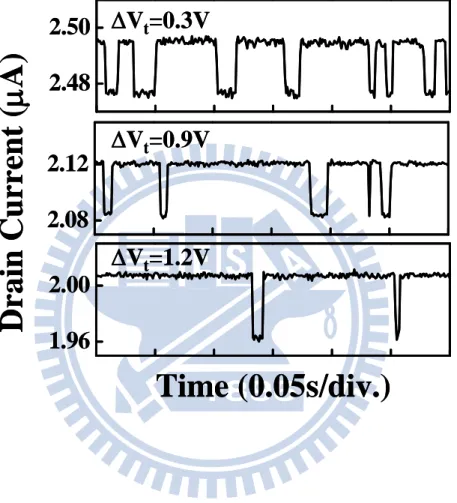
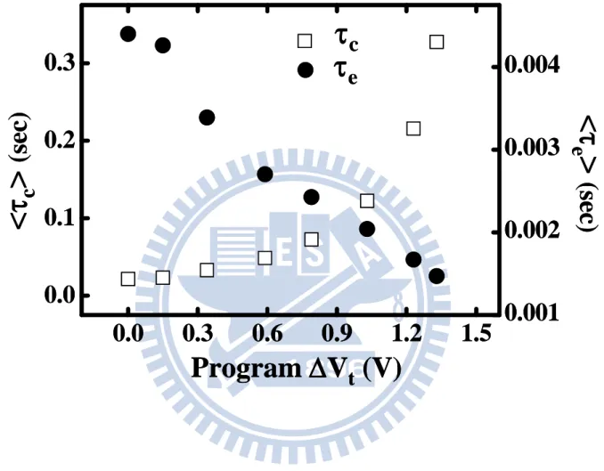
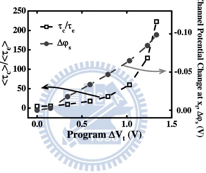
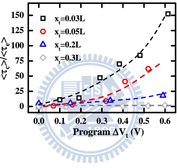
To profile the lateral charge distribution by CHE programming, four SONOS cells are used with a respective trap position at xt=0.03L, 0.05L, 0.2L and 0.3L from the drain junction. Fig. 2.4 shows RTS traces of the channel current at three program ΔVt(=0.3V, 0.9V, 1.2V) in the xt=0.2L cell. The RTS measurement is fixed at Vgs=3.5V and Vds=0.05V. The device is in strong inversion at the measurement biases. Fig. 3.5 shows measured average capture time <τc> and emission time <τe> versus program ΔVt. The minimum integration time is 0.5ms and the total sampling period is 10s. The observed trends in the <τc> and <τe> versus program ΔVt are similar to previous results [2.18]. The ratio of average capture time to emission time <τc>/<τe> and a corresponding surface potential change (Δϕs) at xt from Eq. (2) are plotted in Fig. 2.6. As more electrons are injected into the nitride layer, the conduction band-edge at xt and the trap level move upward with respect to the Fermi level. Thus, the <τc>/<τe> ratio increases with ΔVt. The measured <τc>/<τe> versus ΔVt in the four cells are shown in Fig. 2.7. For a xt closer to the drain junction, for example, the xt=0.03L cell,
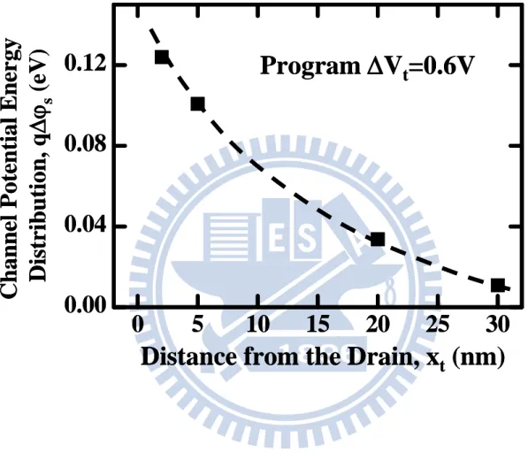
the τc/τe ratio increases more rapidly with ΔVt, implying a higher program charge density at the trap position xt=0.03L. In contrast, the τc/τe remains almost unchanged in the xt=0.3L cell, which means the injected program charge does not reach the trap point during program. The surface potential energy change along the channel for a program window of ΔVt=0.6V is presented in Fig. 2.8. The program charge induced potential barrier is within 30nm. Our result is consistent with most of published results from the inverse I-V method [2.4-2.6] and from Monte Carlo simulation [2.6], [2.19].
2.3.3 CHE versus CHISEL programming
To compare the width of injected charge by CHE and CHISEL program [2.18], a SONOS cell having a trap at xt=0.2L is used. The device is programmed by CHE first. The ratio of τc/τe versus a program ΔVt is recorded. Then, the device is erased and re-programmed by CHISEL. In CHISEL program, a substrate bias of -2V is applied. Fig. 2.9 shows the evolution of τc/τe with ΔVt by CHE and CHISEL. The τc/τe ratio increases more quickly by CHISEL than by CHE. This means that the local channel potential at xt=0.2L is affected by injected charge earlier in CHISEL program as ΔVt increases. In other words, the program charge has a broader distribution in CHISEL than in CHE program at the same program ΔVt. Our findings here are consistent with the result in [2.20]
2.3.4 CHE Program/BTBT Erase Charge Mismatch
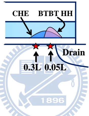
In this section, we discuss the lateral misalignment between CHE program electrons and BTBT erase holes. To this purpose, we choose two devices with a trap
located at the position of 0.05L and 0.3L, respectively, from the drain junction. The two devices are programmed by CHE and then erased by BTBT hot holes. Fig. 2.10 and Fig. 2.11 show the evolution of the τc/τe during program and erase in the two devices. The τc/τe increases with a program ΔVt and then decreases during erase. In Fig. 10, our monitor point is at xt=0.05L in the channel. The τc/τe curves during program and erase match reasonably well, suggesting that program electrons at 0.05L can be totally neutralized by erase holes. To examine the charge polarity in erase state, the τc/τe near ΔVt=0V is re-drawn in a log scale in the inset of Fig. 2.10. The erase-state τc/τe is actually lower than its value in a fresh state. This result provides evidence of hole accumulation near the drain junction in erase state. This phenomenon becomes more pronounced in an over-erased cell, i.e., ΔVt<0V. On the contrary, in Fig. 2.11 where the monitor point is at xt=0.3L, the τc/τe ratio is significantly above its original value after a P/E cycle. The larger τc/τe value after one P/E cycle implies the existence of some residual program electrons at xt=0.3L although the cell has been erased to its original Vt. Combining the results in Figs. 2.10 and 2.11, the charge distributions in program and in erase are depicted in Fig. 2.12. A misalignment of injected erase holes and program electrons [2.11], [2.21] is concluded. The erase holes have a narrower spatial distribution than CHE program electrons.
2.3.5 Program Charge Retention Loss
Two types of models have been published to explain the observed program-state Vt retention loss in a SONOS cell. The first one is nitride charge vertical loss through P/E cycling induced oxide traps [2.22]-[2.26]. The second type of the models explains the Vt retention loss by lateral redistribution of nitride charges
in program state [2.27]-[2.30]. The possibility of program electron lateral movement [2.30] is explored by the RTS method in Fig. 2.13. The cell has only one-time program and then is subject to high temperature bake. The trap position is at 0.03L from the drain. The result shows that the τc/τe remains the same during the bake, indicating that the program electron concentration is unchanged. Another explanation for a program-state Vt loss is nitride trapped hole lateral migration. A three-pole electron-hole-electron distribution in program state has to be assumed in the hole lateral migration models [2.27]-[2.29]. We use the RTS method to examine the charge polarity along the channel in program state. The trap position (monitor point) in measured devices spreads from the drain junction to 0.4L into the channel. We measured program-state and erase-state RTS at different P/E cycles. Fig. 2.14 shows the program-state and erase-state τc/τe versus P/E cycles in an xt=0.05L device. At other xt, the τc/τe dependence on P/E cycle has a similar feature and the result is not shown here. The cycle number in Fig. 2.14 is 16. The reason is that RTS becomes unclear at more P/E cycles due to new interface trap creation. In our monitored range of P/E cycles, program-state τc/τe is always above its original value, showing a negative charge polarity in all the measured cells. We do not find any evidence of positive charge (hole) accumulation in program state. Although there is no sign of hole accumulation within 10-20 P/E cycles. However, we would like to point out that a program-state charge profile may vary with operation biases, device doping profile and P/E cycling conditions [2.29]. Although there is no sign of hole accumulation within 10-20 P/E cycles in the present cycling and bias conditions, we still observe an apparent charge retention loss in these cells under a gate stress condition (Vg=-5V) in Fig. 2.15. The τc/τe ratio decreases with gate stress time. RTS traces immediately after
program and after 4 seconds gate stress are presented in the inset of Fig. 2.15. The τc/τe ratio decreases with gate stress time in Fig. 2.15. Since hole accumulation and lateral movement have been excluded in the cell, the observed decrease of the τc/τe is attributed to charge vertical loss, i.e, stored electron emission through the bottom oxide. Fig. 2.16(a) shows the read current variation versus gate stress time in a 33 P/E cycled cell. The setup for this measurement is shown in Fig. 2.16(b) [2.14]. An electronic switch is used to record gate stress time accurately. The sampling rate is 10kHz, which enable the observation of read current switching with time resolution up to 0.1ms. Both RTS and long-term nitride charge escape are both observed. Individual nitride charge loss is manifested by a long-term abrupt increase of a read current. During two consecutive nitride charge escapes, RTS is observed. It should be stressed that the “average” read current level remains constant between two consecutive nitride charge escapes. This stepwise evolution characteristic provides an evidence of the vertical charge loss. In Fig. 2.17, the retention result is shown in a uniform FN program/erase NAND SONOS cell. In such a device, charge lateral movement should be excluded. But we still observe a clear step-wise current evolution during retention. The feature is pretty much the same as Fig. 2.16(a). These jumps can be explained by a single charge vertical loss plus the percolation effect. If the charge lateral migration is dominant, the current evolution should be “GRADUAL" rather than “ABURPT" since the ΔId due to single-step charge hopping in the lateral direction should be very small.
One major argument in [2.28] against the vertical loss model is “the bottleneck of the carrier loss is either the tunneling or the Frenkel-Poole detrapping”. This argument is incorrect since they do not consider the re-capture of nitride conduction
band electrons into nitride traps before tunneling out through the bottom oxide. By taking into account the re-capture process, we showed [2.31] that even in the Frenkel-Poole (FP) emission limited condition (i.e., Frenkel-Poole emission time longer than oxide tunneling time) the nitride charge retention time can be approximated by 1/ 2 ( ) ( ) ( / ) ( ) ~ exp ( ) e c c T ox ox FP FP E q qF retention FP kT τ τ πε τ τ τ τ ⎛ ⎞ + − = ⎜ ⎟ ⎝ ⎠ (3)
where τe(FP) and τc(FP) are the Frenkel-Poole emission and capture times. τox is an oxide tunneling time, or more specifically, positive oxide trapped charge (hole) assisted tunneling time. F is an electric field in nitride. Other variables have their usual definitions. The above equation can well explain many salient features of the observed program-state Vt retention loss, for example, log dependence on retention time [2.22],[2.26],[2.35] and P/E cycle number ([2.35], Fig. 2.9 in [2.33]), negative dependence on gate stress voltage polarity [2.23],[2.26],[2.34], positive dependence on retention temperature [2.22],[2.26],[2.27]. The comparison of the model predictions from Eq. (4) and experimental results is summarized in Table 2.1. It should be remarked that trap anneal effect during high temperature bake is not considered in Eq. (4). Thus, a deviation between the model and measurement results in the temperature dependence is expected. Although the charge vertical loss model can explain the above measurement results well, other Vt retention loss mechanisms may co-exist in different operation bias or device process conditions.
a low P/E number because of cycling induced new interface trap creation. The RTS measurement result in Fig. 14 does not exclude the possibility of hole accumulation and thus a dipole formation in a heavily cycled cell, or in other device process conditions [2.29].
2.4 Summary
We have demonstrated a novel RTS method to characterize program and erase charge lateral spread in a SONOS flash memory without the need to know a doping profile. In the RTS method, the τc/τe is very sensitive to program/erase/retention charges. It exhibits an exponential dependence on a local potential, as compared to a linear dependence in the CP method. The RTS method can provide a better resolution than a charge pumping method or an inverse I-V modeling approach. A mismatch between program electrons and erase holes is shown by this method. Read current instability due to nitride charge vertical loss and random telegraph noise is directly observed.
ΔI
dτ
cτ
ex
t source drainV
tsx
t source drainV
tsΔI
dτ
cτ
ex
t source drainV
tsx
t source drainV
tsFig. 2.1 Illustration of a two-level RTS waveform resulting from electron emission and capture at an interface trap. τc and τe are electron emission time and capture time. The trap position is xt from the drain junction. The channel potential right below the trap is denoted by Vts.
3.15
3.3
3.45
3.6
0.01
0.1
1
V
d= 0.3V
V
d= 0.05V
Gate Voltage (V)
Cap
ture
Ti
me
,
<
τ
c
>
(sec)
ΔV
ts
3.15
3.3
3.45
3.6
0.01
0.1
1
V
d= 0.3V
V
d= 0.05V
Gate Voltage (V)
Cap
ture
Ti
me
,
<
τ
c
>
(sec)
ΔV
ts
Fig. 2.2 The gate voltage dependence of average capture time in RTS at two drain voltages, Vds=0.05V and 0.3V. The lateral shift of these two curves corresponds to ΔVts.
0.0
0.2
0.4
0.6
0.8
1.0
0
1
2
3
4
5
6
Number of Devices
source
drain
Trap Position,
x
tL
(1-
)
0.0
0.2
0.4
0.6
0.8
1.0
0
1
2
3
4
5
6
Number of Devices
source
drain
Trap Position,
x
tL
(1-
)
Fig. 2.3 Cumulative trap position distribution along the channel. L=0.1μm is the channel length and xt is the distance of a trap from the drain.
2.48
2.50
2.08
2.12
1.96
2.00
Time (0.05s/div.)
Drain Current (
μA)
ΔV
t=0.3V
ΔV
t=0.9V
ΔV
t=1.2V
2.48
2.50
2.08
2.12
1.96
2.00
Time (0.05s/div.)
Drain Current (
μA)
ΔV
t=0.3V
ΔV
t=0.9V
ΔV
t=1.2V
Fig. 2.4 RTS patterns at three program ΔVt=0.3V, 0.9V and 1.2V in a CHE program cell. The RTS measurement condition is Vgs=3.5V and Vds=0.05V. xt =0.2L.
0.0
0.3
0.6
0.9
1.2
1.5
0.0
0.1
0.2
0.3
0.001
0.002
0.003
0.004
τ
c
τ
e
<
τ
c
>
(sec
)
<τ
e
>
(sec
)
Program
ΔV
t
(V)
0.0
0.3
0.6
0.9
1.2
1.5
0.0
0.1
0.2
0.3
0.001
0.002
0.003
0.004
τ
c
τ
e
<
τ
c
>
(sec
)
<τ
e
>
(sec
)
Program
ΔV
t
(V)
Fig. 2.5 Average capture time (τc) and emission time (τe) versus program ΔVt in an xt =0.2L cell.
0.0
0.5
1.0
1.5
0
50
100
150
200
250
τ
c/
τ
eΔϕ
sProgram
ΔV
t
(V)
<
τ
c
>/
<
τ
e
>
Ch
an
n
el Poten
tial Ch
ange at
x
t, Δϕ
s(V)
-
0.10
-
0.05
0.00
0.0
0.5
1.0
1.5
0
50
100
150
200
250
τ
c/
τ
eΔϕ
s0.0
0.5
1.0
1.5
0
50
100
150
200
250
τ
c/
τ
eΔϕ
sProgram
ΔV
t
(V)
<
τ
c
>/
<
τ
e
>
Ch
an
n
el Poten
tial Ch
ange at
x
t, Δϕ
s(V)
-
0.10
-
0.05
0.00
Fig. 2.6 The ratio <τc>/<τe> and a local surface potential change (Δϕs) at the trap position (xt =0.2L) versus program ΔVt. The local potential change is calculated from Eq. (2).
0.0
0.1
0.2
0.3
0.4
0.5
0.6
0
25
50
75
100
125
150
x
t=0.03L
x
t=0.05L
x
t=0.2L
x
t=0.3L
Program
ΔV
t
(V)
<
τ
c
>/<
τ
e
>
0.0
0.1
0.2
0.3
0.4
0.5
0.6
0
25
50
75
100
125
150
x
t=0.03L
x
t=0.05L
x
t=0.2L
x
t=0.3L
Program
ΔV
t
(V)
<
τ
c
>/<
τ
e
>
Fig. 2.7 Evolutions of <τc>/<τe> with program ΔVt at four different trap positions xt=0.03L, 0.05L, 0.2L and 0.3L.
0
5
10
15
20
25
30
0.00
0.04
0.08
0.12
Program
ΔV
t=0.6V
Distance from the Drain, x
t(nm)
Channe
l P
o
te
nt
ia
l Ener
gy
Distr
ibuti
on,
q
Δϕ
s(e
V
)
0
5
10
15
20
25
30
0.00
0.04
0.08
0.12
Program
ΔV
t=0.6V
Distance from the Drain, x
t(nm)
Channe
l P
o
te
nt
ia
l Ener
gy
Distr
ibuti
on,
q
Δϕ
s(e
V
)
Fig. 2.8 The channel potential energy distribution extracted from RTS. The CHE program window is ΔVt=0.6V. The width of the potential energy barrier is about 20nm.
0.0
0.2
0.4
0.6
0.8
1.0
1.2
0
20
40
60
80
100
CHE
CHISEL
x
t=0.2L
<
τ
c
>/<
τ
e
>
Program
ΔV
t
(V)
0.0
0.2
0.4
0.6
0.8
1.0
1.2
0
20
40
60
80
100
CHE
CHISEL
x
t=0.2L
<
τ
c
>/<
τ
e
>
Program
ΔV
t
(V)
Fig. 2.9 Comparison of <τc>/<τe> evolutions with program ΔVt in CHE and CHISEL program. A substrate bias of -2V is applied in CHISEL program.
0.0
0.2
0.4
0.6
0
15
30
45
60
prog.
erase
x
t=0.05L
Program
ΔV
t
(V)
<
τ
c
>/
<
τ
e
>
0.0 0.1 0.2 0.3 0.4
10
-210
-110
010
1ΔV
t(V)
<
τ
c>/
<
τ
e>
0.0
0.2
0.4
0.6
0
15
30
45
60
prog.
erase
x
t=0.05L
Program
ΔV
t
(V)
<
τ
c
>/
<
τ
e
>
0.0 0.1 0.2 0.3 0.4
10
-210
-110
010
1ΔV
t(V)
<
τ
c>/
<
τ
e>
Fig. 2.10 The <τc>/<τe> versus program ΔVt during CHE program and BTBT hot hole erase. The device has a trap at 0.05L from the drain. The inset shows the <τc>/<τe> in a log scale.
0.0
0.2
0.4
0.6
0.5
1.0
1.5
2.0
program
erase
x
t
=0.3L
Program
ΔV
t
(V)
<
τ
c
>/<
τ
e
>
0.0
0.2
0.4
0.6
0.5
1.0
1.5
2.0
program
erase
x
t
=0.3L
Program
ΔV
t
(V)
<
τ
c
>/<
τ
e
>
Fig. 2.11 The <τc>/<τe> versus program ΔVt during CHE program and BTBT hot hole erase. The device has a trap at 0.3L from the drain.
Drain
0.05L
0.3L
CHE
BTBT HH
Drain
0.05L
0.3L
CHE
BTBT HH
Fig. 2.12 Illustration of program/erase charge distributions in the channel. The stars represent interface traps. The program electrons at xt=0.05L are completely compensated, but some far electron at xt=0.3L are not compensated by erase holes.

![Fig. 1.3 Estimation of threshold voltage shift as a function of process node [1.30]](https://thumb-ap.123doks.com/thumbv2/9libinfo/8451871.182552/29.892.213.691.452.855/fig-estimation-threshold-voltage-shift-function-process-node.webp)