國立交通大學
材料科學與工程學研究所
碩士論文
利用 SF
6/O
2電漿對氮化鋁鎵/氮化鎵高電子遷移率電晶
體閘極掘入區域進行後處理之探討
Study of SF
6/O
2Plasma Post-Treatment for
the Recess of AlGaN/GaN HEMTs
研究生 林渼璇
指導教授 張 翼 博士
利用SF
6/O
2電漿對氮化鋁鎵/氮化鎵高電子遷移率電晶體閘
極掘入區域進行後處理之探討
Study of SF
6/O
2Plasma Post-Treatment for
the Recess of AlGaN/GaN HEMTs
研 究 生:林渼璇 Student: Mei-Hsuan Lin
指導教授:張 翼 博士 Advisor: Dr. Edward Yi Chang
國立交通大學
材料科學與工程研究所
碩士論文
A Thesis Submitted to Department of Materials Science and Engineering College of Engineering
National Chiao Tung University In Partial Fulfill of the Requirements
For the Degree of Master of Science
In Material Science and Engineering July 2007
Hsinchu, Taiwan, Republic of China
中華民國九十六年七月
Content
Abstract (Chinese) ... Ⅰ
Abstract (English) ··· Ⅲ
Acknowledge ...Ⅴ
Content ... Ⅵ
Table Captions ... Ⅸ
Figure Captions ... Ⅹ
Chapter 1 Introduction
1.1 General Background ... 1
1.2 Dissertation Content ... 2
Chapter 2 Literature Review
2.1 Dry Etching of Ш Nitrides Materials ... 5
2.2 Recessed AlGaN/GaN HEMT ... 6
2.3 Improvement on Plasma Damage of Recess Etching ... 7
2.4 Trap Effect and Pulse I-V Measurement ... 8
Chapter3 Fundamentals of Electrical Characteristics
and XPS Analysis
3.1 Schottky Characteristics of Schottky Diodes ... 11
3.1.1 I-V Characteristics ... 11
3.2 Pulse Measurement ... 12
3.3 X-ray Photoelectron Spectroscopy Analysis (XPS) ... 14
Chapter4 Experiment
4.1 Schottky Diodes ... 19
4.1.1 BCl3 Recess Etching ... 19 4.1.2 SF6/O2 Plasma Post-Treatment ... 20 4.1.3 I-V, C-V Measurement ... 204.2 Device Fabrication ... 20
4.2.1 Wafer cleaning ... 21 4.2.2 Mesa isolation ... 214.2.3 Ohmic contact formation ... 21
4.2.4 Lithography of T-gate ... 22
4.2.5 Gate recess ... 22
4.2.6 Post-Treatment and Gate Deposition ... 23
4.3 DC Characteristics Measurements... 23
4.4 Pulse characteristics Measurements ... 23
4.5 RF Characteristics Measurements ... 24
4.6 Material Analysis ... 25
4.6.1 AFM samples preparation and measurement ... 25
4.6.2 XPS samples preparation and measurement ... 25
Chapter5 Results and Discussion
5.1 Recess Etching on Schottky Diodes ... 27
5.1.1 BCl3 Recess Etching ... 27
5.1.2 SF6/O2 Plasma Post-Treatment ... 29
5.1.3 Combination of Recess Etching and Plasma Post-Treatment.. 30
5.2 Recessed HEMT with and without Fluorine Plasma
Post-Treatment ... 31
5.2.1 Device DC Characteristics ... 31
5.2.2 Device RF Characteristics ... 32
5.2.3 Device Pulse I-V Characteristics ... 33
5.3 Material Analysis ... 34
5.3.1 Atomic Force Microscopy (AFM) ... 34
5.3.2 X-ray Photoelectron Spectroscopy (XPS) ... 34
Chapter6 Conclusion ... 52
Table Captions
Table
1-1
Comparison between material parameters for Si, GaAs, SiC and GaN at T= 300 K ... 4Table 5-1
2DEG location and estimated BCl3 recess etching depth by the C-V measurement ... 36Table 5-2
The ideality factor and Schottky barrier height (SBH)Schottky diodes with and without different SF6 post-treatments. ... 36
Table 5-3
Comparison of off-state breakdown voltage and gate-drain leakage current of different HEMT devices ... 37Table 5-4
Comparison of small-signal characteristics on differentHEMT devices ... 37
Table 5-5
Comparison of current recovery using pulse I-V measurement ... 37Table 5-6
Comparison of the surface roughness measured using AFM ... 37Table 5-7
Results from the XPS measurement on various plasma-treated samples ... 38Figure Captions
Fig. 2-1 Schematic diagram of ICP etching system ... 10
Fig. 2-2 Schematic of configuration of dry etching of a semi-conducting sample ... 10
Fig. 3-1 The method of pulsed IV measurement. ... 17
Fig. 3-2 The method of detecting surface trap. ... 17
Fig. 3-3 The scheme of current recovery calculation. ... 18
Fig. 4-1 Cross-section of Recessed AlGaN/GaN HEMT. ... 26
Fig. 4-2 The flow chart of the process flow. ... 26
Fig. 5-1 I-V characteristics of Schottky diodes exposed to BCl3 plasma as a function of etching time prior to deposition of the rectifying contact. 39 Fig. 5-2 Schottky barrier height and ideality factor of Schottky diodes which exposed to BCl3 plasma as a function of etching time. ... 39
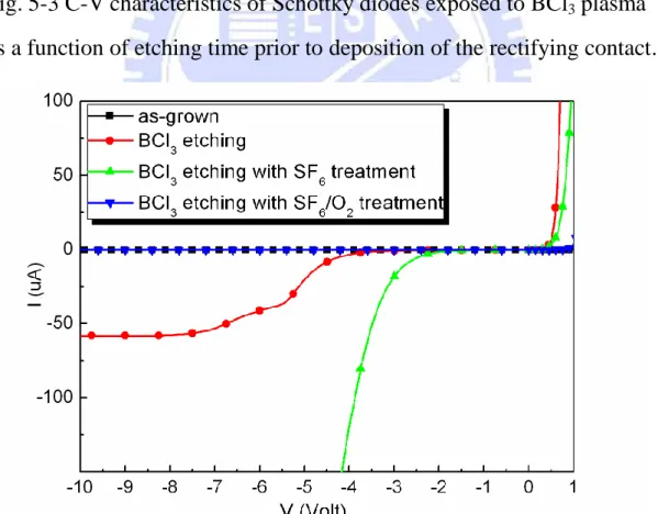
Fig. 5-3 C-V characteristics of Schottky diodes exposed to BCl3 plasma as a function of etching time prior to deposition of the rectifying contact. ... 40
Fig. 5-4 I-V characteristics of Schottky diodes which are at first exposed to BCl3 plasma and then respectively exposed to SF6 and SF6/O2 plasma ... 40
Fig. 5-5 The Schottky reverse leakage current of Schottky diode at different ratios of O2 to SF6 ... 41
Fig. 5-6Threshold voltage characteristic of Schottky diode at different ratios of O2 to SF6 ... 41 Fig. 5-7 Variation of the threshold voltage on BCl3 recessed Schottky diodes exposed to SF6/O2 plasma post-treatment as a function of
treatment time. ... 42 Fig. 5-8 I-V characteristics of BCl3 recessed Schottky diodes exposed to SF6/O2 plasma post-treatment as a function of treatment time. ... 42 Fig. 5-9 I-V characteristics of 5µm gate-drain spacing conventional HEMT ... 43 Fig. 5-10 Typical DC transfer characteristics of conventional HEMT... 43 Fig. 5-11 I-V characteristics of 5µm gate-drain spacing BCl3 recessed HEMT ... 44 Fig. 5-12 Typical DC transfer characteristics of BCl3 recessed HEMT . 44 Fig. 5-13 I-V characteristics of 5µm gate-drain spacing BCl3 recessed HEMT with SF6/O2 post-treatment ... 45 Fig. 5-14 Typical DC transfer characteristics of BCl3 recessed
HEMT with SF6/O2 post-treatment ... 45 Fig. 5-15 Comparison of off-state breakdown voltage of conventional HEMT, BCl3 recessed HEMT with and without post-treatment. ... 46 Fig. 5-16 Small-signal microwave characteristics of conventional HEMT. ... 46 Fig. 5-17 Small-signal microwave characteristics of BCl3 recessed HEMT. ... 47 Fig. 5-18 Small-signal microwave characteristics of BCl3 recessed HEMT with SF6/O2 post-treatment. ... 47 Fig. 5-19 Pulsed IV characteristics of conventional HEMT which bias point are (VD=0 V and VG= 0 V) and (VD=0 V and VG= -6 V) ... 48
Fig. 5-20 Pulsed IV characteristics of BCl3 recessed HEMT which bias point are (VD=0 V and VG= 0 V) and (VD=0 V and VG= -6 V) ... 48
post-treatment which bias point are (VD=0 V and VG= 0 V) and (VD=0 V
and VG= -6 V) ... 49
Fig. 5-22 AFM measurement before etching, Rrms=0.324 nm ... 49 Fig. 5-23 AFM measurement after BCl3 recess etching, Rrms=0.427 nm 50 Fig. 5-24 AFM measurement after BCl3 recess etching and SF6/O2 plasma post-treatment , Rrms=0.94 nm ... 50 Fig. 5-25 The estimated band diagram after BCl3 etching ... 51
利用 SF
6/O
2電漿對氮化鋁鎵/氮化鎵高電子遷
移率電晶體閘極掘入區域進行後處理之探討
研究生: 林渼璇 指導教授: 張 翼 博士 國立交通大學材料科學與工程學系摘要
閘極掘入是改變閘極與電流通道的距離而使截止電壓改變,進而 使電晶體的表現最佳化,閘極掘入的技術已經廣泛的應用在三五族半 導體裡。在三五族半導體砷化鎵的元件,閘極掘入的蝕刻多半使用濕 式化學蝕刻;但是由於氮化鎵材料本身化學惰性大,沒有辦法使用一 般濕式化學蝕刻,於是電漿乾式蝕刻就被應用在蝕刻氮化鎵材料上, 同時也帶來在主動區電漿損害的問題。 此論文主要提出利用 SF6/O2電漿的後處理,對氮化鋁鎵/氮化鎵高 電子遷移率電晶體閘極掘入區域進行後處理,目的在於減輕乾式蝕刻 所帶來的損害。 本實驗利用蕭基二極體去模擬元件閘極經過後處理過後的表 現。觀察在不同電漿處理下逆向漏電流以及截止電壓的變化,了解電 漿後處理對蕭基特性影響程度,進而尋找一個最佳化的後處理條件。 將最佳化的後處理條件應用在氮化鋁鎵/氮化鎵高電子遷移率電 晶體,並且製作 SF6/O2電漿後處理閘極掘入之氮化鋁鎵/氮化鎵高電子遷移率電晶體,其最大互導係數為 160 mS/mm 且具有高於 100 V 的
崩潰電壓。在高頻特性上展現了 23 GHz 的截止頻率(fT)與 62 GHz 的
最高震盪頻率(fmax)。與沒有處理過的元件相比,閘極掘入的高電子
遷移率電晶體經過電漿後處理,具有較高的崩潰電壓以及良好的電流
Study of SF
6/O
2Plasma Post-Treatment
for the Recess of AlGaN/GaN HEMTs
Student: Mei-Hsuan Lin Advisor: Dr. Edward Y. Chang
Department of Materials Science and Engineering National Chiao Tung University
Abstract
Gate recess is widely used in III-V compound transistors to modify the threshold voltage and optimize the device performance through adjusting the gate to channel distance. The recess in GaAs based HEMTs is done using wet chemical etching. On the other hand, recess of GaN based devices is usually achieved using dry etching due to the chemical inertness of the material to the chemicals. However, this leads to the problem of plasma damage in the active region of the device and this degrades the device performance.
In this thesis, a post-treatment method using SF6/O2 plasma is proposed and applied for the fabrication of BCl3 recessed AlGaN/GaN high electron mobility transistors (HEMTs) to alleviate the damages related to the dry etch.
The condition of the SF6/O2 plasma post-treatment was first investigated using Schottky diodes. Reverse leakage current and the threshold voltage shift were monitored to understand the effect of different plasma treatments. An optimized post-treatment condition was found to have decreased the Schottky reverse leakage current by three orders of magnitude and minimized the threshold voltage shift.
This condition was then applied to the AlGaN/GaN HEMTs. The fabricated 0.8μ m ×200 μ m BCl3 recessed AlGaN/GaN HEMT with SF6/O2 post-treatment exhibited a maximum transconductance of 160 mS/mm with an off-state breakdown voltage of more than 100 V. The cutoff frequency fT and maximum oscillation frequency fmax were 23 GHz and 62 GHz respectively. Compared to the untreated HEMTs, the recessed HEMT devices with the proposed post-treatment have demonstrated higher breakdown voltage and better pulse current recovery.
致謝
從大學專題研究到現在,在這個實驗室經歷了三年的歲月,從一 開始懵懂無知的小朋友一點一滴地進步,學習如何做實驗、操作儀 器、遇到問題如何解決、報告技巧以及與人溝通的方法,一路上要感 謝太多太多的人。首先,要先感謝的就是張翼教授,老師您含辛茹苦 的把這個實驗室的從什麼都沒有到現在擁有豐富的實驗資源和儀器 設備,讓我們擁有最優質的學習研究環境,提供我們充分學習的環境。 另外就是要感謝 GaN 小組的每一個同伴,黃瑞乾學長、呂宗育學 長、張家達學長還有蕭世匡學弟,因為有你們的幫助與存在,我才成 長。不論是做實驗還是做人處世方面,一旦遇到艱難的問題,你們就 像家人一樣,永遠給予我最大的幫助,即使心情不好,待在 405 就可 以感受到大家的活力與快樂,感謝小噴和宗育讓 405 的歡笑不斷,新 成員匡匡學弟,謝謝你剛進來時每天不斷的接受我的荼毒,當然還有 阿乾學長,謝謝你一直以來無怨無悔地看我很糟糕的報告以及指導我 實驗的方向,總之,謝謝大家忍受我三年來的無知與任性還有許多許 多的糊塗。 我很喜歡這個實驗室,雖然曾經遇到很多問題,最後真的很開心 能夠在這裡與所有的朋友認識。一直以來接受大家的幫助,真心感謝 吳偉誠學長、褚立新學長、陳克弦學長、張家源學長、郭建億學長、許立翰學長、黃延儀學長、黃珍嬅學姊曾經對我的指導,還有一起奮 鬥的胡吟竹同學、曾文仲同學、唐士軒同學,常常聽我抒發生活上以 及實驗上的不順。還有許許多多的學弟妹們,謝謝你們在畢業典禮時 給我們最真誠的祝福,多謝曾郁玲學妹、王景德學弟、曾志偉學弟、 鐘榮濤學弟、黃曼琪學妹、施琳琪學妹、謝勝禮學弟、黃偉進學弟、 蕭佑霖學弟,因為你們的幫忙,我們才可以在碩二時專心做自己的實 驗而免於一些實驗室雜務。最後,謝謝親愛的助理小姐們 Cherry、 Serena、還有我們最專業的管理技術人員詹前章先生、黃碧玉小姐和 李芳銘先生,一直以來在行政事務上的幫助,當然還有情感上的抒 發,跟你們聊天真的很快樂,謝謝大家。 最後感謝一直在背後無怨無悔支持我的男朋友和我親愛的家 人,你們是我永遠的支柱。
Chapter 1
Introduction
1.1 General Background
In the recent decades, GaN and its alloy compounds have attracted much studies for applications in our daily life due to their superior properties such as chemical inertia, wide direct energy bandgap (3.4 eV), high breakdown (2×10⁶ V/cm), high saturation velocity (2.2×107 cm/s) and large power density compared to other materials. The comparison of the several substrates material properties is shown in Table 1-1. These advantages enable GaN compound semiconductors to be applied into some specific areas where the conventional compound or Si semiconductors can not be used【1】. The common applications of GaN based alloys are optoelectronic devices such as light emitting diodes (LED), laser diodes (LD)【2-3】, and power amplifiers such as high voltage Schottky rectifiers, heterojunction bipolar transistors (HBTs) and high electron mobility transistors (HEMT).
Owing to the excellent material properties of GaN, the applications of AlGaN/GaN high electron mobility transistors (HEMTs) are focused on high frequency, high power and high temperature applications. The improvement in material growth and processing techniques has produced the GaN devices with performances superior to that of GaAs and InP power devices. However, the transconductance property which is important for low-power consumption driving has not been improved dramatically【4】. Therefore, recessed gate technique which is generally used in GaAs and InP devices
can be employed to develop to improve the performance of the GaN devices. For the conventional III-V recess etching process, two major methods were used; one is chemical wet etching and another is plasma dry etching. However, due to high bonding energy and low chemical reactivity of GaN compound semiconductors, wet etching is not easy for GaN as compared to the conventional GaAs semiconductors. Although photoenhanced chemical (PEC) wet etching【5】 has been demonstrated for GaN etching, alkaline solution can etch or dissolve the photo-resist easily. This kind of wet etching is therefore not suitable for the GaN HEMT fabrication, especially for the critical process such as gate recess. For these reasons, the plasma dry etching is considered as a better approach for the etching of GaN materials.
But surface damage caused by plasma dry etching results in the deterioration of the device performances such as lower breakdown voltage and higher leakage current. Therefore, the reduction of plasma damage becomes a main issue for gate recess process. Recently, there are many methods proposed for the reduction of residual plasma damages, such as adding CH4 and O2 into conventional Cl2/Ar plasma【6】, using CF4/O2 to reduce plasma damage【7】, and pre/post annealing process【8-10】. In this study, we focused on SF6/O2 plasma post-treatment after dry etch recess at the recess region to reduce plasma damages.
1.2 Thesis Content
The contents of this thesis include: literature review, fundamentals of electrical characteristics, experiment, results, discussions and conclusions. In Chapter 2, the literature survey on the characteristics of recessed AlGaN/GaN HEMT and fluorine plasma post-treatment are reviewed. In
Chapter 3, the fundamentals of electrical characteristics and XPS analysis are addressed. In Chapter 4, the recess etching process, the samples preparation for material analysis, and the BCl3 recessed AlGaN/GaN HEMT device process flow and the SF6/O2 plasma post-treatment process are described. In Chapter 5, Schottky characteristics after different plasma exposures and the recessed HEMT device performances with SF6/O2 plasma post-treatment are discussed. Finally, the conclusions will be given in Chapter 6.
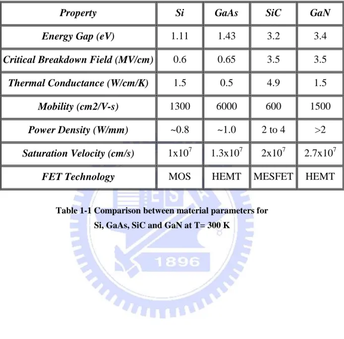
Property Si GaAs SiC GaN Energy Gap (eV) 1.11 1.43 3.2 3.4
Critical Breakdown Field (MV/cm) 0.6 0.65 3.5 3.5
Thermal Conductance (W/cm/K) 1.5 0.5 4.9 1.5
Mobility (cm2/V-s) 1300 6000 600 1500
Power Density (W/mm) ~0.8 ~1.0 2 to 4 >2
Saturation Velocity (cm/s) 1x10⁷ 1.3x10⁷ 2x10⁷ 2.7x10⁷
FET Technology MOS HEMT MESFET HEMT
Table 1-1 Comparison between material parameters for Si, GaAs, SiC and GaN at T= 300 K
Chapter 2 Literature Review
2.1 Dry Etching of Ш Nitrides Materials
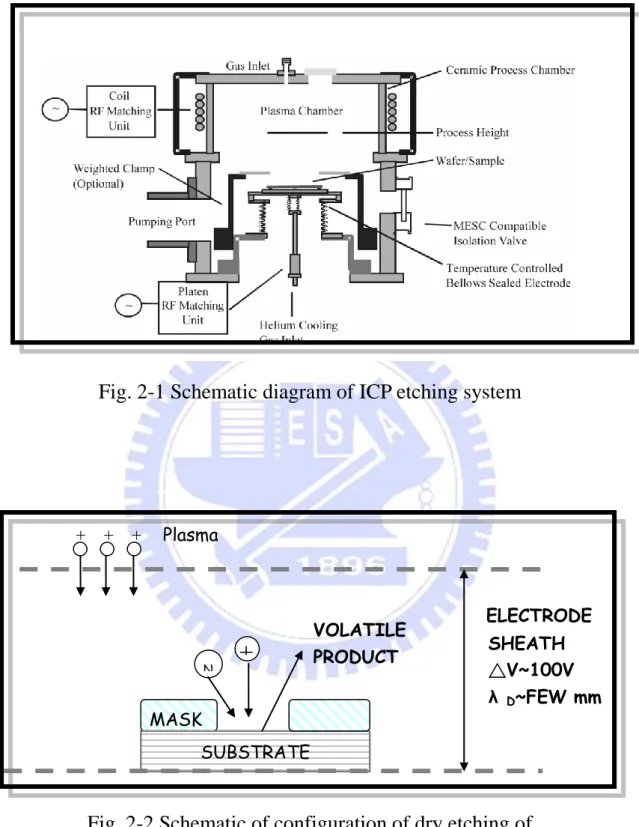
Fabrication of the wide range of new electronic optical-electronic devices envisioned for the gallium nitride material system will require the development of entirely new processing procedures. The group Ш nitrides are distinguished by their unusual chemical stability, a characteristic that has posed unique challenges for device processing. Due to the extreme resistance of the group Ш nitrides to chemical attack by conventional wet etchants, the etching rate of the dry etching is much higher than the wet etching. Hence, etching nitride films has been carried out almost entirely using dry etching methods. These techniques include reactive ion etching (RIE), magnetron enhanced RIE (MERIE), electron cyclotron resonance (ECR), chemically assisted ion beam etching (CAIBE), and inductively coupled plasma (ICP). Fig 2-1 shows the basic scheme of ICP system.
The basic principle of these methods is similar, i.e. etching occurs through a combination of both chemical and physical means. Reactive neutral atoms of chlorine, iodine, bromine or other elements produce chemical etching by forming volatile products. Physical removal of material by sputtering is produced by impinging ions. The combination of the two mechanisms is able to produce anisotropic etching at practical rates but with varying degrees of damages. A schematic representation of the reaction around the sample during plasma etching is shown in Fig 2-2. The body of plasma is neutral, containing equal numbers of electrons and
ions (~5x1011 cm-3), but is at a positive potential with respect to the sample. Ions in the plasma that stray near the sheath region (where electrons are excluded by the negative potential of sample position) are accelerated across it and strike the sample at near vertical incidence. Neutral reactive gas atoms and molecules which constitute the most prevalent state in plasma (~3x1013cm-3 at 1 mTorr) are also incident on the surface. Volatile etch products formed by adsorption and reaction of these species with the sample materials are removed by ion assisted processes at more rapid rate than would occur in the absence of ion bombardment. Sputter assisted removal of these etch products exposes a fresh surface for the following chemical process to occur, and in this fashion there is a synergy between chemical and physical etch mechanisms.
2.2 Recessed AlGaN/GaN HEMT
Following the advancement in the nano-technology, reducing gate length is one of the most effective ways to increase the HEMT speed. However, the main problem of scaling down the gate length is short channel effect. In HEMT devices, if the barrier layer is thick or the gate length is extremely short, the aspect ratio between gate length and barrier thickness becomes critically important. In general, the aspect ratio becomes a problem when it is less than 5. And when this happens, it will shift the threshold voltage to more negative part which means harder to turn off the channel. This is so-called ―short channel effect.‖ To scale down the gate length and avoid short channel effect, gate recess technique
is applied to solve the problem. The so-called ―gate-recess‖ technique is to reduce the thickness of the barrier layer under the gate metal.
For conventional III-V compound semiconductor, such as GaAs- based HEMT, there are many chemical wet-etching recipes that can be applied to recess etching. The major advantage of wet etching is low damages. However, it is difficult to find a compatible wet etching method for AlGaN/GaN HEMT. As an alternative approach, a chloride-based inductively coupled plasma reactive ion etching (ICP) has been employed to fulfill such tasks by several groups. 【 6-8 】 This approach can effectively modify the threshold voltage of AlGaN/GaN HEMT to positive direction. However, the induced damages and the associated defects lead to an increase in Schottky reverse leakage current. Larger Schottky reverse leakage current would lower the breakdown voltage of the HEMT devices.
2.3 Improvement on Plasma Damage of Recess Etching
Because there are limited wet etching possibilities on GaN, a significant effort has been devoted to various dry etching techniques. As reported, plasma-induced damage has degraded the device performances such as more leakage current. Because of the methods have been suggested to reduce plasma-induced damage such as pre/post Rapid Thermal Annealing (RTA) and post-plasma treatment【7-10】. However, annealing at high temperature during the RTA is not compatible with the gate metal (Ni/Au, for example) and has to be carried out prior to the gate deposition or the high temperature would cause gate metal to react with
Schottky layer. As a result, photoresist has to be removed after the recess etching and followed by a second photolithography step for the gate electrode. Thus, the gate electrode and the recess etching are not self-aligned. To avoid a large access resistance that could be caused by the ungated recess region, the gate electrode is required to be larger than the recess window. For this reason, plasma post-treatment seems to be a better method to recover plasma-induced damage. It has been reported that CF4/O2 plasma treatment between the processes of the gate recess and gate metallization can reduce leakage current induced by plasma damage.【7】 But the reason why CF4 plasma can recover plasma damage is not yet clarified.
2.4 Trap Effect and Pulse I-V Measurement
Since the demonstration of the first GaN based transistor, rapid progress has been made in the development of GaN-based HEMT devices. Output powers of over 100 W have already been reported up to 6 GHz 【 11 】 . However, the existence of dispersion effects observed in
GaN-based devices has limited the initial expectations. The presence of trapping centers in GaN based transistor which is related to surface, material, or interface states, has been considered as the main cause of these effects【12-13】. Some of the observed effects are current collapse, transconductance frequency dispersion, gate-lag, drain-lag transients, and limited microwave power output. Up to now it has not been possible to obtain concise conclusions of the inner mechanisms explaining the
behavior of the devices due to the presence of surface states.
Pulse measurements have already been applied to electronic device characterizations such as pulsed I-V and pulsed power measurement. The main reasons for using the pulse characterizations can be attributed to the need to investigate the trapping carriers and device heating effects. In the consideration of trapping carrier, the response time of these trapping carriers is the main reason to affect the performance of pulse measurement. Generally speaking, the response time of these trapping carriers are in μsec ~ msec level, which is obviously slower than the nsec level of electron carriers transportation especially for the high speed devices. Therefore, it is needed to check the behaviors of trapping carriers to prevent the slow response time of the trapping carriers that affecting the RF performance. Because high mobility electron transistor (HEMT) is a kind of horizontal devices and its channel is also very close to the surface of the device. It always shows more serious surface trapping effect than BJT devices, and pulse measurements are important characterization methods to detect the trapping effect in HEMT 【14-16】. Additionally, the heating effect in high speed electronic is also an important issue for the application of power amplifier. The pulse measurement provides a very low dc power consumption to operate the device, and the heating effect can be observed by using various pulse widths to measure the device I-V curve. Therefore, the pulse measurement has become more important than the traditional dc measurement especially for the microwave power device, where there is always a serious heating effect on the device under test (DUT).
Fig. 2-1 Schematic diagram of ICP etching system
Fig. 2-2 Schematic of configuration of dry etching of a semi-conducting sample SHEATH △V~100V λ D~FEW mm SUBSTRATE MASK VOLATILE PRODUCT Plasma N + + + + ELECTRODE
Chapter 3
Fundamentals of Electrical
Characteristics and XPS Analysis
3.1 Schottky Characteristics of Schottky Diodes
3.1.1 I-V Characteristics
Schottky contact characteristics of Schottky diodes are directly related to the gate performances of HEMT devices. One can take account of some Schottky parameters including Schottky barrier height ΦB and the ideality factor n to simulate the gate performance. Calculations of the Schottky barrier height ΦB and the ideality factor n can be achieved using the Richardson Equation below and fitted by the forward I-V characteristic:
Is: saturation current, n: ideal factor, A: diode area, A*: effective Richardson constant, k: Boltzmann’s constant, and T: absolute temperature.
exp
1
nkT
qV
I
I
s kT q T AA I b S
exp 2 * * 2 3 / * 2 qm k h A
3.1.2 C-V Characteristics
The purpose for C-V measurement is to find out the shift of threshold voltage and the location of 2DEG. The relation between carrier
concentration and capacitance is shown below:
dC
dV
q
C
C
dV
d
q
x
n
o s o s
3 1 21
2
V: Voltage applied on Schottky gate metal, C: the measured capacitance,
ε s: material dielectric constant, ε o: 8.5x10
-14
C/V-cm
And the relation between depletion depth and capacitance is shown below
C
x
s
oWe could use the above two formulas to estimate the etching depth of BCl3 recess etching.
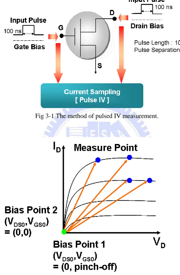
3.2 Pulse Measurement
This method is described in Fig.3-1. Pulse I-V measurement is acquired with a short pulse (100 ns pulse width) and a pulse separation (1 ms separation). The pulsed IV characteristics are suggested to detect the device performance under the isothermal conditions of device operation【17】.Therefore pulse measurement is always used for observing
the surface state.
A high-density distribution of surface states which act as electron traps located in the access regions between the metal contacts could cause the gate-lag effect. The trapped electrons depleted the 2-DEG in the access regions of the device, thereby limiting the current. The effect of surface trap was characterized using pulse IVs as shown in Fig. 3-2 at two extrinsic quiescent biases equivalent to:
1. Bias Point (gate-off): VGS0 < VPinch , VDS0 = 0 V 2. Bias Point (gate-on): VGS0 = 0 V, VDS0 = 0 V
Using these two quiescent bias conditions, the drain current variation could be assumed to be related to the surface trap, since this effect is mainly stimulated by the gate voltage【18】.
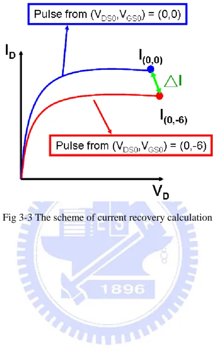
Following this, there is a formula brought up to represent the degree of surface trap:
From the phenomenon of surface trap, if there is less surface trap, there is better current recovery. If not, there is worse current recovery.
And the definition of the current recovery is shown in Fig 3-3 and the following formula:
ery
Current
trap
Surface
cov
Re
1
) 0 , 0 ( ) 6 , 0 ( ) 0 , 0 ( ) 0 , 0 ( ) 6 , 0 ( ) 0 , 0 (1
1
cov
Re
I
I
I
I
I
I
I
ery
Current
3.3
X-ray Photoelectron Spectroscopy
Analysis (XPS)
The X-ray Photoelectron Spectroscopy also known as XPS or ESCA (Electron Spectroscopy for Chemical Analysis) has been developed since the fifties by Professor K. Siegbahn. The Physical Nobel Prize was awarded to his work in 1981.
The most interesting thing with this technique is its ability to measure binding energy variations resulting from their chemical environment. That is, information on the chemical nature and state of the detected elements at the sample surface. The theory of determination of chemical bonding of XPS is based on the equation below:
(
)
(
)
(
)
(
)
)
(
i
l
i
qk
i
V
ij
Er
i
BE
i
: the electron orbit which emits the photoelectron,)
(i
BE
: total binding energy)
(i
l
: binding energy at neutral condition (element)q
: charge)
(i
k
: constant)
(ij
V
: electron potential energy from other atoms within the molecule)
(i
Er
: relaxation energyAs the atoms are bonded, valence electrons form the bonds. Then the energy states of the atoms will change to make the atoms deviate from the neutral. The difference in electron affinities will make some atoms more positively charged and the others more negatively charged than neutral. The positive charged Q is added to the total binding energy and peak
shifts to higher binding energy, and vice versa. The higher oxidation state also has higher electron binding energy since it is more positive. As a result, XPS is a powerful tool to study the chemical bonding and oxidation state.
The basic of XPS is X-ray induced photoemission. When the specimen atom absorbs a photon from the X-ray source, it gains the energy of the photon and released a photonelectron to regain its original stable energy state. The released electron retains all the energy from the striking photon. It can then escape from the atom, and even further from the matter and the kinetic energy keeps it moving which can be described by the following equations:
Z ph
hv
E
E
ph
E : The kinetic energy of photo electron; hv: Incident X-ray photo
energy; EZ: The binding energy of specimen atom.
As for solid state material, work functionΦ is added to represent the energy of an electron escape from the surface. Hence the equation is modified as below:
Z phhv
E
E
The incident photon energy of X-ray sources usually used in XPS is Al Kα 1486.6 eV and Mg Kα 1253.6 eV. In our experiment, we use the
Mg Kα X-ray source. Upon the released of X-ray induced photo
electrons the atoms will be lacking of electrons in the internal shells. To recover from this ionized state the atoms can emit another photon
(fluorescence) or undergo an Auger transition and result in Auger electron signals. We must distinguish the XPS and Auger signals in the spectrum. One way to distinguish these two kinds of peaks is to change the X-ray source since the kinetic energy of the Auger electron is independent of the source but kinetic energy of photoelectrons is depending on the source.
There is a severe problem called ―charging‖ that occur among insulator and wide bandgap semiconductors. While the photoelectrons escape from specimen, if there aren’t enough electrons flow into specimen to maintain electrical neutrality, the specimen tends to be positively charged and resulted in a peak shift toward higher binding energy. We can use a flood gun to inject low energy electron to the surface to neutralize the charges. But most of the times the problem can be very complicated. To modify the flood gun current may be not very easy. The worst situation happens when Ar ion sputtering is used for depth profiling of insulators. Ar ions can charge and may also react with the surface, which make it difficult to identify. Coating a thin conducting film on insulator specimen and ground it could be an effective way to avoid charging. We can also take Au 4d3/2= 353 eV as a reference while scanning.
Fig 3-1 The method of pulsed IV measurement.
Chapter 4 Experiment
4.1 Schottky Diodes
The studies of Schottky diodes include BCl3 recess etching, SF6/O2 plasma post-treatment and the combination of both of them.
The fabrication of Schottky diodes begins with a standard photolithography which was used to pattern the substrates for ohmic metal. Ti (20 nm)/ Al (120 nm)/ Ni (25 nm)/Au (100 nm) ohmic metal was then deposited on the substrates using an electron-beam evaporator at a pressure of ~1x10⁻⁶ Torr. The bulk of the resist and metal were then removed by a wet solvent lift-off process, following by a high pressure DI water rinse to remove the residues. After the lift-off, the samples were annealed using RTA at 800℃ for 60sec. Then, a second photolithography was used to pattern the Schottky gate metal.
4.1.1 BCl
3Recess Etching
For highly sensitive region under the gate, a smooth surface with low damage should be achieved after recess etching. To find the recess etching condition, we fabricated Schottky diodes to observe the Schottky reverse leakage current. Before the Schottky gate metal deposition, we used BCl3 plasma to etch the Schottky gate region. Then the Ni (20 nm)/ Au (50 nm) gate metal was deposited by electron-beam evaporator.
4.1.2 SF
6/O
2Plasma Post-Treatment
SF6/O2 plasma post treatment was applied after the BCl3 recess etching but before the gate metal deposition. There were many different ratios of O2 to SF6 used to observe the change of the Schottky characteristics of O2/SF6 ratio. The other conditions for the treatment are:the applied power was 50 W;the pressure was 10 mT;the flow of SF6 was kept constant at 20 sccm.
4.1.3 I-V, C-V Measurement
I-V and C-V measurements were used to check the Schottky characteristic after the BCl3 recess etching and the SF6/O2 plasma post-treatment. Here, we used HP4156b and HP4280 to measure the I-V and C-V characteristics of Schottky diodes, respectively.
4.2 Device Fabrication
The epitaxial layers of the AlGaN/GaN high electron mobility transistors (HEMT) were grown by metal-organic chemical vapor deposition (MOCVD) on sapphire substrate along the (0001) axis. The schematic cross-sectional view of our AlGaN/GaN HEMT structure is shown in Fig. 4-1. The MOCVD grown AlGaN/GaN HEMT structure consists of a 3μ m-thick undoped GaN buffer layer and a 30 nm undoped
AlGaN Schotty layer with Al composition of 30%. Room temperature
cm2/V-s, respectively.
The detailed fabrication process on the recessed AlGaN/GaN HEMT device with SF6/O2 plasma post-treatment is described at the following sections. Besides, the conventional HEMTs and recessed HEMTs without post-treatment were also fabricated for comparison. The flow chart of the process flow for device fabrication is shown in Fig. 4-2.
4.2.1 Wafer cleaning
The wafers were immersed in Acetone (ACE) and isopropyl alcohol (IPA), each for five minutes to remove contamination from the wafer surface, and then the wafers were blown dry by nitrogen gas.
4.2.2 Mesa isolation
Here, we used AZ5214E photoresist to define the active region. The mesa isolation was carried out by using Cl2/Ar plasma dry etching in the STS Inductive Coupled Plasma (ICP) system. The ICP dry etching condition was :Coil power 450 W, platen power 150 W, and Cl2/Ar=20/2 sccm at 10 mTorr. The etching depth was checked by the
α -step measurement.
4.2.3 Ohmic contact formation
After the mesa etching, we also used the AZ5214E photoresist to define the ohmic contact region. Before transferring into the electron-beam evaporator, the wafers were descummed and immersed
into HCl: H2O=1:10 solution for five minutes to remove the surface oxides. Ti (20 nm)/ Al (120 nm)/ Ni (25 nm)/Au (100 nm) ohmic metal was then deposited on the substrates using an electron-beam evaporator at a pressure of ~1x10⁻⁶ Torr. The bulk of the resist and metal were then removed by a wet solvent lift-off process, followed by a high pressure DI water rinse to remove the residues. After the lift-off process, a rapid temperature annealing (RTA) process at 800℃ for 60sec was conducted to form the ohmic contact.
4.2.4 Lithography of T-gate
For high frequency and high speed application, short gate length with low gate resistance is desired. The T-shaped gate structure is the most common approach for obtaining low gate resistance. In the T-gate structure design, the gate length is defined by the small footprint and the wide top offers low gate resistance.
To obtain a T-gate, we used a double photo-resist structure consisting of Copolymer for the bottom layer and PMMA for the top layer.
4.2.5 Gate recess
After patterning the T-shaped gate, the exposed HEMT active layers were etched to achieve the desired channel current and pinch-off voltage characteristics. This process was done by dry etch technique (STS-ICP system). The etching condition was: platen power 50 W, BCl3 10 sccm, 23 mTorr.
4.2.6 Post-Treatment and Gate Deposition
Following the recess etching process was the post-treatment process. The post-treatment process was also done by STS-ICP system. The condition of the post-treatment was: platen power 50W, SF6/O2=20/2sccm, 10mTorr.
After the post-treatment process, the gate metal Ni (20 nm) / Au (200 nm) were consequently deposited using an electron-beam evaporator at a pressure of ~1x10⁻⁶ Torr. After the evaporation, the resist and metal were then removed using a wet solvent lift-off process, followed by a high pressure DI water rinse to remove the residues.
Electrical Characteristics Measurement
After the device fabrication process, DC, RF and pulse performance of the AlGaN/GaN HEMT was measured using the on-wafer measurement.
4.3 DC Characteristics Measurements
For the DC measurement, the I-V characteristics were obtained using an HP4156b Modular DC Source/Monitor.
4.4 Pulse characteristics Measurements
Pulse I-V measurement of AlGaN/GaN HEMT device was done using the ACCENT DIVA dynamic I-V analyzer, where both the gate and drain of the HEMT were pulsed on top of the DC bias conditions.
The devices were measured at two extrinsic quiescent biases equivalent to:
1. Bias Point (gate-off): VDS0 = 0 V , VGS0 = -6 V 2. Bias Point (gate-on): VDS0 = 0 V , VGS0 = 0 V ,
Using these two quiescent bias conditions, the drain current variation was assumed to be related to the surface trap.
4.5 RF Characteristics Measurements
Scattering parameters
The S-parameters of the AlGaN/GaN HEMT devices were measured by HP8510 Vector Network Analyzer using the on-wafer GSG probes from Cascade MicroTech. The S-parameters were measured in the frequencies ranging from 0.4 to 40.4 GHz. Cutoff frequency (fT) and maximum frequency of oscillation (fmax) of the devices were characterized. These two quantities represent the unity gain intercept point of the short circuit current gain (h21) and the unilateral power gain (U). Each parameter can be computed from the S-parameter data.
The h21 as a function of frequency were measured under drain voltage (Vd) of 3~15V. The f
T was extrapolated with -20 dB/decade slope.
4.6 Material Analysis
4.6.1 AFM samples preparation and measurement
Samples were immersed in the Acetone (ACE) and then the isopropyl alcohol (IPA), each for five minutes, and blown dry by nitrogen gas. After that, a BOE: H2O= 1:10 solution was applied to remove the surface oxide. These samples were then divided into three groups. The first one was without any recess etching and post-treatment on the gate region which was used as a reference for others. The second one was treated in BCl3 plasma recess etching for 40 seconds in the ICP system. The third one was treated the same as the second one but following by a SF6/O2 post-treatment for 20 seconds. Then, the surface morphology was measured by Veeco MultiMode Scanning Probe Microscope (MMAFM)
4.6.2 XPS sample preparation and measurement
The XPS sample preparation was the same as AFM samples. Prior to XPS analysis, a very thin Au film was deposited by the electron-beam evaporator for better current conductivity and as a reference in the spectrum analysis. That is because during the XPS measurement, peaks position may shift due to localized surface charging. In order to distinguish the chemical-shift from the charging-shift, the Au peaks were needed as a reference.
Once the samples were prepared, they were measured using Thermo VG Scientific’s Microlab 350 System for XPS measurement.
Fig. 4-1 Cross-section of Recessed AlGaN/GaN HEMT.
Chapter 5 Results and Discussion
In this chapter, we will first discuss the effects of BCl3 recess etching and SF6/O2 plasma treatment on the performance of the Schottky diodes. These two steps will then be combined to achieve the optimized condition for gate recess etching. After that, the optimum condition is used to fabricate the recessed AlGaN/GaN HEMT device. The DC, RF performance and the pulse measurement results of the three different types of devices i.e. conventional HEMT, recessed HEMT, and recessed HEMT with post-treatment will be compared. Finally, the effect of SF6/O2 plasma post-treatment on the gate leakage current will also be investigated based on the XPS analysis.
5.1 Recess Etching on Schottky Diodes
In this study, smooth surface was achieved using BCl3 plasma etching in the STS ICP system. The condition for BCl3 recess etching was:platen power 50 W, pressures 23 mTorr and BCl3 flow 10 sccm. The morphology of the etched surface was checked by AFM and the results are as shown in the part of material analysis (section 5.3.1).
5.1.1 BCl
3Recess Etching
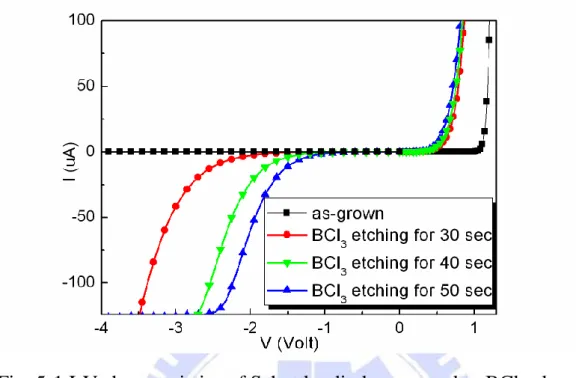
Schottky diodes were fabricated and were used to observe the effect of the recess etching on the device performances. Fig. 5-1 shows the I-V characteristics of the Schottky diodes by increasing the recess etching
time from 30 sec to 50 sec. At etching time of 30 sec, the reverse leakage current had dramatically increased from 2 µA to 250 µA at 15 V. As a result of plasma induced damages, the reverse leakage current of the Schottky diodes became worse with longer plasma exposure. Fig. 5-2 shows the parameters of the Schottky diodes calculated from the Schottky forward I-V characteristic. The larger ideality factor and lower Schottky barrier height with increasing etching time were resulted from the plasma damage.
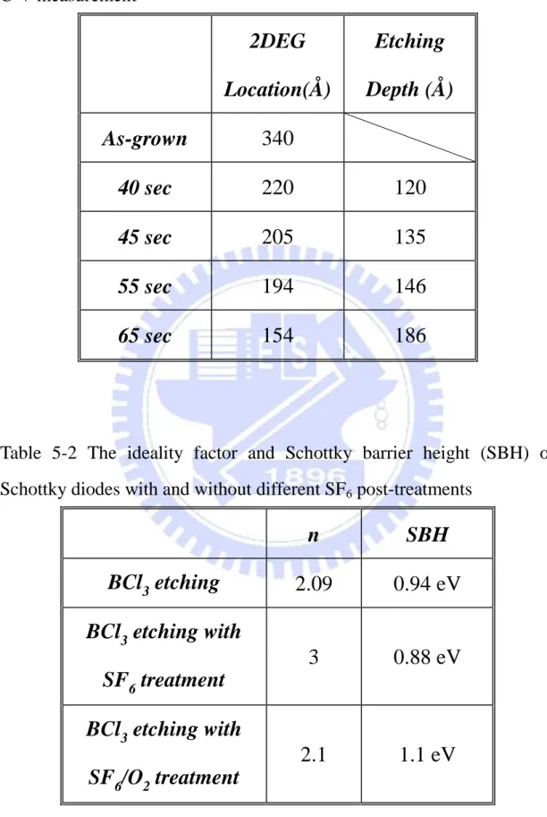
Besides, in order to find out the relationship between the etching time and the etching depth, C-V measurements for Schottky diodes with different etching time was carried out. Fig. 5-3 illustrates the C-V characteristics of the diodes with different etching time. Drastic change of threshold voltage from -4.5 V to -2.8V was observed with 40 sec etching. Furthermore, with increasing etching time, the threshold voltage moved to more positive side. We also found that with increasing etching time the higher capacitance from 4 pF to 10 pF was observed. This is because the capacitance is an inverse ratio to the distance. With shorter distance, the capacitance will be higher. Table 5-1 shows the calculated 2DEG location from the equation of C-V capacitance. Change of 2DEG location with etching time meant the AlGaN was etched away. For this reason, we can use the calculated 2DEG location to estimate the etching depth. The estimated etching depth is illustrated at the last column of Table 5-1. Owing to increasing plasma damage with exposure time, proper etching depth with proper etching time should be chosen【19】. As a result, a
following research.
5.1.2 SF
6/O
2Plasma Post-Treatment
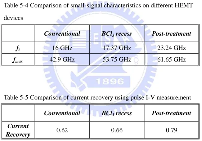
It was due to the plasma damage that larger Schottky reverse leakage current and non-ideal Schottky characteristics were observed after the BCl3 recess etching. In order to reduce the plasma damage, fluorine-base plasma post-treatment was carried out. I-V characteristics of the Schottky diodes with fluorine plasma post-treatment are shown in Fig. 5-4. The results showed that with pure SF6 plasma post-treatment, the Schottky reverse leakage current became larger. But with O2 added into the SF6, great improvement on the diode performance was observed with the leakage current reduced from 58 µA to 80 nA and Schottky barrier height increased from 0.94 eV to 1.1 eV (Table 5-2). With O2 plasma addition, same ideality factor and higher barrier height of 1.1 eV were observed after plasma etch which were suggested to be the reason for leakage current reduction.
In order to figure out how the ratio of O2 to SF6 affecting the Schottky diode characteristics, different ratios of O2 to SF6 plasma post-treatment were used. In all cases, the post-treatment time was the same. These results are illustrated in Fig. 5-5. With O2 addition, all the Schottky diodes showed better reverse leakage current by two to four orders as compared to the sample without the post-treatment. What’s more, where the ratio O2 to SF6 equal to 0.6, the Schottky reverse leakage current reduced to 10 nA, which was the lowest among the samples. However, from the change of threshold voltages observed from the C-V measurement as shown in Fig. 5-6, the threshold voltage shift after the
plasma treatment with O2/SF6 ratio of 0.6 was 1.1 V. It can be concluded that with the O2/SF6 ratio of 0.6, lowest Schottky reverse leakage current was obtained, however the big shift of the threshold voltage made it unsuitable for practical application. As a result, the O2/SF6 ratio of 0.1 was chosen as the post-treatment condition because it reduces the Schottky reverse leakage current by two orders and with only small shift of the threshold voltage least.
5.1.3 Combination of Gate Recess Etching and Plasma
Post-Treatment
As discussed earlier, the results of recess etching experiment suggested that the BCl3 etching time of 40 sec and the O2/SF6 ratio of 0.1 for post-treatment were the best process conditions. These two conditions were used to investigate for the gate recess of the devices. Fig. 5-7 and Fig 5-8 show the C-V and I-V Schottky characteristics by changing the SF6/O2 post-treatment time. It was found that the O2/SF6 ratio of 0.1 affected the threshold voltage least; further increasing the treatment time to 30 seconds, the shift of the threshold voltage can be as high as 0.7 V. On the other hand, with increasing SF6/O2 post-treatment time, better recovery of Schottky reverse leakage current of 60 nA was observed. In order to obtain an optimized condition for the gate recess etching, a post-treatment time of 20 sec was chosen to achieve the least shift in threshold voltage of 0.45 V meanwhile with an improvement in leakage current of three orders of magnitude.
5.2 Recessed HEMT with and without Fluorine Plasma
Post-Treatment
After the devices were fabricated, DC, RF and pulse performances of the AlGaN/GaN HEMT were characterized using the on-wafer measurement. For the DC measurement, the I-V characteristics were obtained easily by using an HP4156b Modular DC Source/Monitor. The S-parameters of RF performance for AlGaN/GaN HEMT devices were measured by HP8510 Vector Network Analyzer using the on-wafer GSG probes from Cascade MicroTech. The Pulsed I-V characteristics for the AlGaN/GaN HEMT device were measured by ACCENT DIVA dynamic I-V analyzer.
5.2.1 Device DC Characteristics
Three AlGaN/GaN HEMT devices were fabricated. The first one was conventional HEMT device without any treatment, the second one was BCl3 recessed HEMT, and the third one was BCl3 recessed HEMT with SF6/O2 plasma post-treatment. DC characteristics of the 200 µm gate width AlGaN/GaN HEMT with gate length of 0.8 µm, source and drain spacing of 5µm were measured after fabrication. Fig. 5-9 to Fig. 5-14 show the I-V characteristics and the peak extrinsic transconductance of the HEMTs with different post-treatment. The saturation currents at 0 V bias gate voltage of conventional HEMT, BCl3 recessed HEMT and BCl3 recessed HEMT with SF6/O2 plasma post-treatment were 557 mA/mm, 445 mA/mm, 450 mA/mm, respectively. And the corresponding peak
extrinsic transconductances, gm, were 147 mS/mm, 155 mS/mm, and 160 mS/mm, respectively. After BCl3 recess etching, the saturation current was decreased from 557 mA/mm to 445 mA/mm which was attributed to a thinner and the polarization effect of AlGaN layer. In contrast, the peak extrinsic transconductance increased to 155 mS/mm, which was owing to the shift of threshold voltage from -4.5V to -3.5 V. Post-treatment on the recessed HEMT showed better saturation current and peak extrinsic transconductance. Damage recovery might be the reason for the improved performances.
Off-state breakdown voltage and gate-drain leakage current were also measured on the conventional, BCl3 recessed with and without SF6/O2 plasma post-treatment AlGaN/GaN HEMTs. The off-state breakdown voltage was defined by 1mA/mm drain leakage current at the pinch-off gate voltage. Comparison of off-state breakdown voltage of the above devices is shown in Fig. 5-15. After BCl3 etching, the off-state breakdown voltage had dropped to 90 V, possibly due to the plasma damage. On the other hand, with SF6/O2 plasma post-treatment, the breakdown voltage was improved to beyond 100V. It could be said that post-treatment recovered the plasma damage during etching process. Furthermore, the gate-drain leakage current was obviously improved from 0.3031 mA/mm to 0.0043 mA/mm. The above values are listed in Table 5-3 for comparison.
5.2.2 Device RF Characteristics
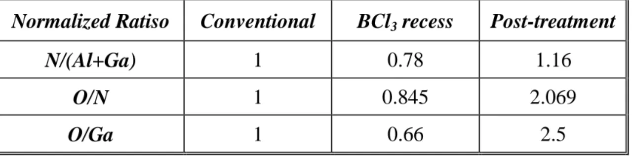
The S-parameters for the HEMT devices were measured from 0.4 to 40.4 GHz by HP8510 Vector Network Analyzer using the on-wafer 150-μm-pitch GSG probes from Cascade MicroTech. Fig. 5-16 to Fig. 5-18 show the frequency dependence of the current gain H21, power gain MAG/MSG, and unilateral gain U of the different treated HEMT devices. The current gain, cut-off frequency fT and the maximum oscillation frequency fmax obtained for the above devices are listed in Table 5-4 for comparison. Slightly increase of cut-off frequency fT and maximum frequency fmax from 16 to 17 GHz and from 42 to 53 GHz for the conventional HEMT and the recessed HEMT were observed, respectively. It is likely that recess structure could have lowered the output conductance and feedback capacitance under the gate region【20-21】. Further improvement of ft to 23 GHz and fmax to 61 GHz after post-treatment was attributed to plasma damage recovery.
5.2.3 Device Pulse I-V Characteristics
Synchronized gate and drain pulses on the same bias point (using Accent-Diva) were characterized for pulse I-V measurement. Therefore, the pulsed IV characteristics could be used to detect surface state under the isothermal conditions of device operation. The results are depicted in Fig. 5-19, Fig. 5-20, and Fig. 5-21. From the formula stated in section 3.2, the degree of current recovery was computed, and listed in Table 5-5. Current recovery of the conventional HEMT was increased to 0.66 after BCl3 recess etching, and further increased to 0.79 after SF6/O2 plasma
post-treatment. No Si3N4 passivation was applied to the above devices. As a result, these devices were all without surface protection. Therefore, better current recovery of recessed HEMT might be attributed to improved gate control efficiency and reduced gate lag effect. All the improvements were observed after SF6/O2 plasma post-treatment. This can be explained by the damage recovery upon the post-treatment.
5.3 Material Analysis
5.3.1 Atomic Force Microscopy (AFM)
AFM measurements on surface roughness of the three samples, before etching, BCl3 etching and BCl3 etching with SF6/O2 plasma post-treatment are shown in Fig. 5-22, Fig. 5-23 and Fig. 5-24. No significant change in surface roughness was discovered. The root-mean-square surface roughness remained less than 1 nm for all samples. The values of root-mean-square surface roughnesswere listed in Table 5-6 for comparison.
5.3.2 X-ray Photoelectron Spectroscopy (XPS)
Three samples, as-grown, BCl3 etching, BCl3 etching with SF6/O2 plasma post-treatment, were prepared to evaluate the surface chemistry using XPS. Photoelectrons from the AlGaN surface were detected at an escape angle of 60° to make it more surface-sensitive. The elements of Al, Ga, N, F and O were detected on all the samples to determine the surface composition. Table 5-7 summarizes the surface composition of AlGaN as derived from the XPS data.
The XPS results can be interpreted as following. The ratio of N to Ga and Al decreased to 0.78 after BCl3 etching. Loss of nitrogen was responsible for the increase of nitrogen vacancies. That was because nitrogen atoms were predominantly escaped from the surface during the ICP etching process. The nitrogen-vacancy related defect level above the EF, which was near the conduction-band edge, would ionize and become the dominant positive charged donors in the etched sample. An increase in the positive charge for the extrinsic nitrogen-vacancies defects would lead to an increase in the negative charge in the surface space-charge region, an increase in the surface band bending, and a shift of the surface Fermi level toward the conduction-band edge. The near-surface electronic state of AlGaN is schematized in Fig 5-25. With a thinner Schottky barrier after BCl3 etching it was easier for electron to tunnel. Therefore, higher leakage current was observed. Also, from Table 5-7, there was an increase of oxygen ratio over 2 after SF6/O2 plasma. Oxygen could have occupied the nitrogen-vacancy because of its lower formation energy 【22】.As a result, the nitrogen-vacancy related defects were reduced.
Besides, oxygen might also cause the formation of a thin oxide layer on top of the AlGaN layer【6】. This oxide layer would have raised the Schottky barrier height and reduced the leakage current
Table 5-1 2DEG location and estimated BCl3 recess etching depth by the C-V measurement
2DEG
Location(Å )
Etching
Depth (Å )
As-grown
340
40 sec
220
120
45 sec
205
135
55 sec
194
146
65 sec
154
186
Table 5-2 The ideality factor and Schottky barrier height (SBH) of Schottky diodes with and without different SF6 post-treatments
n
SBH
BCl
3etching
2.09
0.94 eV
BCl
3etching with
SF
6treatment
3
0.88 eV
BCl
3etching with
SF
6/O
2treatment
2.1
1.1 eV
Table 5-3 Comparison of off-state breakdown voltage and gate-drain leakage current on different HEMT devices
Conventional BCl3 recess Post-treatment
Off-state Breakdown Voltage 100 V 90 V > 100 V Gate-Drain Leakage Current 0.207 mA/mm @100V 0.3031 mA/mm @100V 0.0043 mA/mm @100V
Table 5-4 Comparison of small-signal characteristics on different HEMT devices
Conventional BCl3 recess Post-treatment
ft 16 GHz 17.37 GHz 23.24 GHz
fmax 42.9 GHz 53.75 GHz 61.65 GHz
Table 5-5 Comparison of current recovery using pulse I-V measurement
Conventional BCl3 recess Post-treatment
Current
Recovery 0.62 0.66 0.79
Table 5-6 Comparison of the surface roughness measured using AFM
Before Etching BCl3 recess Post-treatment
Table 5-7 Results from the XPS measurement on various plasma-treated samples
Normalized Ratiso Conventional BCl3 recess Post-treatment
N/(Al+Ga) 1 0.78 1.16
O/N 1 0.845 2.069
Fig. 5-1 I-V characteristics of Schottky diodes exposed to BCl3 plasma as a function of etching time prior to deposition of the rectifying contact.
Fig. 5-2 Schottky barrier height and ideality factor of Schottky diodes which exposed to BCl3 plasma as a function of etching time.
Fig. 5-3 C-V characteristics of Schottky diodes exposed to BCl3 plasma as a function of etching time prior to deposition of the rectifying contact.
Fig. 5-4 I-V characteristics of Schottky diodes which are at first exposed to BCl3 plasma and then respectively exposed to SF6 and SF6/O2 plasma
Fig. 5-5 The Schottky reverse leakage current of Schottky diode at different ratios of O2 to SF6
Fig. 5-6Threshold voltage characteristic of Schottky diode at different ratios of O2 to SF6
Fig. 5-7 Variation of the threshold voltage on BCl3 recessed Schottky diodes exposed to SF6/O2 plasma post-treatment as a function of post-treatment time.
Fig. 5-8 I-V characteristics of BCl3 recessed Schottky diodes exposed to SF6/O2 plasma post-treatment as a function of treatment time.
Fig. 5-9 I-V characteristics of 5µm gate-drain spacing conventional HEMT
Fig.5-11 I-V characteristics of 5µm gate-drain spacing BCl3 recessed HEMT
Fig. 5-13 I-V characteristics of 5µm gate-drain spacing BCl3 recessed HEMT with SF6/O2 post-treatment
Fig. 5-14 Typical DC transfer characteristics of BCl3 recessed HEMT with SF6/O2 post-treatment
Fig. 5-15 Comparison of off-state breakdown voltage of conventional HEMT, BCl3 recessed HEMT with and without post-treatment.
Fig. 5-17 Small-signal microwave characteristics of BCl3 recessed HEMT.
Fig. 5-18 Small-signal microwave characteristics of BCl3 recessed HEMT with SF6/O2 post-treatment.
Fig. 5-19 Pulsed IV characteristics of conventional HEMT which bias point are (VD=0 V and VG= 0 V) and (VD=0 V and VG= -6 V)
Fig. 5-20 Pulsed IV characteristics of BCl3 recessed HEMT which bias point are (VD=0 V and VG= 0 V) and (VD=0 V and VG= -6 V)
Fig. 5-21 Pulsed IV characteristics of BCl 3 recessed HEMT with SF6/O2 plasma post-treatment which bias point are (VD=0 V and VG= 0 V) and
(VD=0 V and VG= -6 V)
Fig 5-23 AFM measurement after BCl3 recess etching, Rrms=0.427 nm
Fig 5-24 AFM measurement after BCl3 recess etching and SF6/O2 plasma post-treatment, Rrms=0.94 nm
Chapter6
Conclusions
In this study, a method of SF6/O2 plasma post-treatment has been proposed for the AlGaN/GaN HEMT gate recess process to reduce the damages caused by the plasma etch. The SF6/O2 plasma post-treatment had successfully reduced the Schottky reverse leakage current by 2~3 orders of magnitude with less positive shift in the threshold voltage. The BCl3 recessed AlGaN/GaN HEMTs with SF6/O2 plasma post-treatment had demonstrated higher saturation current of 450 mA/mm and higher peak-transconductance of 160 mS/mm than those without post-treatment. Besides, improvement on the off-state breakdown voltage of more than 100 V was also observed. For the RF performance, better small-signal characteristics of ft =23 GHz and fmax =66 GHz were achieved using the proposed gate recess and post-treatment process. The increased current recovery observed by pulse measurement in the recessed HEMT with post-treatment suggests better gate control and effective plasma damage recovery. And the phenomenon of reduced Schottky reverse leakage current suggests that a thin oxide layer had formed on top of AlGaN layer, which evidenced by the XPS analysis data.