國 立 交 通 大 學
材料科學與工程學系
博 士 論 文
磁阻式元件之磁阻抗及氧化鎢電阻式記憶體的研究
Study of Magneto Impedance for Magneto Resistive
Memory and Tungsten Oxide for Resistive Memory
研 究 生 :簡維志
指導教授 :林鵬 教授
姚永德 教授
中華民國九十九年三月
磁阻式元件之磁阻抗及氧化鎢電阻式記憶體的
磁阻式元件之磁阻抗及氧化鎢電阻式記憶體的
磁阻式元件之磁阻抗及氧化鎢電阻式記憶體的
磁阻式元件之磁阻抗及氧化鎢電阻式記憶體的
研究
研究
研究
研究
博士生 博士生 博士生 博士生 : 簡維志簡維志簡維志簡維志 指導教授指導教授指導教授指導教授 : 林鵬林鵬林鵬林鵬 教授教授教授教授 姚永德姚永德姚永德姚永德 教授教授教授教授 國立交通大學 國立交通大學 國立交通大學 國立交通大學 材料科學與工程學系 材料科學與工程學系 材料科學與工程學系 材料科學與工程學系
摘要
摘要
摘要
摘要
本論文主要研究磁阻式元件之磁阻抗行為及氧化鎢記憶體特性,以求對於電阻式記 憶體的物理特性能有更深入地了解。 磁阻式元件是磁性隨機存取記憶體中扮演相當重要的角色,其中包含類自旋閥元件 及穿隧式磁阻元件。磁阻式元件的直流電性行為已經被廣泛的研究,然而關於交流電性 的行為則是很少被研究。因此在本篇論文的前半部分我們主要探討磁阻式元件的交流特 性。 我們提供了一個藉由類自旋閥的交流特性,來對奈米氧化層在類自旋閥的貢獻做非 破壞性的分析。此外我們以等效電路模型來解釋穿隧式磁阻元件的交流特性,並且在穿 隧式磁阻元件 Ru (5nm) /Cu (10nm) /Ru(5nm) /IrMn(10nm) /CoFeB(4nm) /Al(1.2nm)-oxide /CoFeB (4nm) /Ru (5nm) 發現在很高的交流頻率 17.7 百萬赫茲,此元件的虛部磁阻抗, 有非常劇烈的變化可達 17000%,這個發現使的磁穿隧元件有潛力應用於高頻的感應式元 件。 本論文的後半部分,研究有關於氧化鎢電阻式隨機存取記憶體。由於電阻式隨機存 取記憶體,具有極佳的微縮能力及具備做成三維元件的可能性,所以一直被看好能取代 電子式儲存的記憶體;然而其基礎理論並不完備,且元件的表現還有待更進步。因此我
們提出了一個具新穎性的氧化鎢電阻式隨機存取記憶體,其製作方式只需在現有半導體 製程多一道曝光程序,並且完全符合 CMOS 製程。我們以快速氧化技術所製備的氧化鎢 電阻式隨機存取記憶體,可表現出極佳的元件特性,例如低電流操作、極短時間操作、 好的記憶維持能力及可達百萬次的操作次數。 對於氧化鎢電阻式隨機存取記憶體,我們進一步發現頂部電極的功函數大小可以改 變傳導機制,在低功函數頂部電極其電流傳導機制符合空間電荷限制電流的理論,而在 高功函數頂部電極其電流傳導機制符合熱離子發射理論。此研究提供了藉著改變頂部電 極,有機會改善元件的特性表現。所以根據這個發現,我們設著去研究利用鎳當頂部電 極的氧化鎢電阻式隨機存取記憶體。此新元件表現出非常好的特性,如低於 200 微安培 的操作電流、大於 100 倍的阻值變化及在攝氏 85 度的環境下,大於 300 年的記憶維持 能力。
Study of Magneto Impedance for Magneto
Resistive Memory and Tungsten Oxide for
Resistive Memory
Student : Wei-Chih Chien Advisor : Prof. Pang Lin Prof. Yeong-Der Yao
Department of Materials Science and Engineering National Chiao Tung University
ABSTRACT
This dissertation is devoted to study the magneto impedance effect of magneto resistive elements, and tungsten oxide resistive memory extensively for providing in-depth their physical understanding.
The magneto resistive elements such as pseudo spin valve (PSV) and magneto tunneling junction (MTJ) play a role for magneto random access memory (MRAM). The DC behaviors for magneto resistive elements have been widely studied, but the AC behaviors are still rare. Thus, in the first half of this dissertation we focus on the AC behaviors of magneto resistive elements.
By using AC characteristics, we provide a new non-destructive analysis method to study the nano-oxide layer effects of PSV. Besides, the equivalent circuit model is used to describe the AC behaviors for MTJ. For Ru (5nm) /Cu (10nm) /Ru(5nm) /IrMn(10nm) /CoFeB(4nm) /Al(1.2nm)-oxide /CoFeB (4nm) /Ru (5nm) system, a huge imaginary part of magneto impedance ratio more than 17000% is observed at high frequency 17.7MHz. Magneto impedance effect of the MTJ is potentially a sensitive sensor for high frequencies.
studied extensively. Although resistive random access memory (RRAM) is forecasted to be the promising solutions to replace the electron storage memory due to its excellent scalability and 3D possibility, up to now, the fundamental understanding is still very limited and device performance is required to improve. Thus, we proposed a novel WOX for the RRAM system, because it requires only one extra mask under standard CMOS process. By using rapid thermal oxidation (RTO) for the WOX RRAM, we have demonstrated its good performance such as low switching current, fast programming speed, good thermal stability, and high endurance > 1M times for nonvolatile memory.
Under this study, we further find the work function (WF) of the electrode is a key element determining the conduction mechanism for WOX RRAM. SCLC (space charge limit current) mechanism and thermionic emission mechanism are identified for low WF and high WF electrodes, respectively. These studies imply that the device performance may be significantly improved by selecting the proper electrode. With this guideline, Ni/WOX/W device is investigated. The new Ni/WOX/W device shows very good performance that operates at <200uA switching current, a 100X resistance ratio window, and extremely good data retention of > 300 years at 85 oC.
誌謝
誌謝
誌謝
誌謝
在交大三年多求學的日子,我得到很多人的幫忙及支持,使的我在攻讀博士的生涯 能克服層層的阻礙,並且對於未來的挑戰更有信心去面對。所以這本論文是代表著我對 您們獻上我由衷的感謝,及對我們一起走過不可抹滅的足跡。 首先我要感謝我的母親芳如,您真的很辛苦,獨自一人將我撫養長大,沒有您的支 持讓我無後顧之憂,我今日無法完成我的博士學業,我的學位有一半是屬於您的。我也 要感謝我的叔叔,謝謝您總是對我視如己出也很照顧我母親,您是我決定續續升學的關 鍵,真的很感激您,希望在後半輩子我能好好孝順您和母親。我還要感謝我最摯愛的外 公外婆,我有接近一半的的時間是由您們將我辛苦帶大,看著您們的背影,我學習到人 生其實也可以過的平凡又幸福。 接下來要感謝我的指導教授姚永德老師,從碩士班到博士班這五年多來,很謝謝您 對我的指導及照顧,謝謝您總是對我未來的發展細心的著想,我從您的身上學習到了很 多身為師長的態度,我希望我以後若是有這個機會身為他人的師長,我也能和您看齊。 我要感謝旺宏電子對我的栽培,博士生涯能在前瞻實驗室做研究真的是一件很幸福 的事,有一群很好的夥伴,互相幫忙、互相切磋,這對我的研究,有莫大無比的幫助。 更謝謝逸舟及 Rich 對我博士生涯的磨練及指導,我從您們的身上學習到如何做研究及 做研究該有的態度,也期望在未來我能和前瞻實驗室的夥伴們並肩而立。 我還要感謝一個對我來說很特別的團體,交大羽球隊,謝謝這支球隊提供我一個轉 換心情的場所,能適度排解讀書及工作的壓力,雖然說有時候也會常常測試我的極限, 在我忙不過來的時候,火上加油一番,不過跟你們在一起打球是很快樂的,也謝謝廖威 彰教練對我的指導及照顧,我從您的身上學到了許多做事負責任的道理。 最後要謝謝我的女友巧雯,謝謝妳七年多來的陪伴,讓我在求學生涯有溫柔的避風 港,也多謝妳的鼓勵,讓我在一次接一次的挫折中,能快速的爬起來,我相信在我們未 來的日子裡,我們一定能互相扶持,繼續往我們的人生大步邁進。 我誠摯的感謝曾經幫助過我的人,我以這本論文,代表我對您們獻上的敬意。LIST OF CONTENTS
PageAbstract (Chinese)
………..………...Abstract (English)
………..………Acknowledgement (Chinese)
………..……..………..List of Contents
……….………..List of Figures
……….………..………...Chapter 1: Introduction
………...….... 1.1 Background and Motivation……… 1.2 Thesis Organization………..Chapter 2: Basic of MRAM and RRAM
………. 2.1 Magnetoresistive Random Access Memory (MRAM)…………...……… 2.1.1 Magnetoresistance Effect……….………….…...……… 2.1.2 Magneto Impedance Theory ………..……….. 2.1.3 Field Driven Magnetization Switching Designs……….. 2.1.4 Spin Torque Transfer Driven Switching Designs……… 2.2 Resistive Random Access Memory (RRAM)……….. 2.2.1 Unipolar and Bipolar Behaviors……….………. 2.2.2 Electrochemical Metallization Effect ……….………. 2.2.3 Valency Change Switching Effect ……….………….. 2.2.4 Thermochemical Effect……….………... i iii v vi xi 1 1 3 4 4 4 11 13 16 20 20 21 21 24Chapter 3: Magneto Impedance Study for Pseudo Spin Valves
…….. 3.1 Introduction……….………..…… 3.2 Experiments………... 3.3 Magneto Impedance Behavior and Its Equivalent Circuit Analysis of aCo/Cu/Co/Py Pseudo Spin Valve with a Nano-Oxide Layer ……….. 3.3.1 Equivalent Circuit for Pseudo Spin Valve……… 3.3.2 Magneto Impedance Behavior for Pseudo Spin Valve………
3.3.3 Annealing Effect……….. 3.3.4 Conclusion………... 3.4 Characterization of a Nano-Oxide Layer in a Pseudo Spin Valve by Complex Magneto-Impedance Spectroscopy……… 3.4.1 Magneto Impedance Study for Different Thickness of Bottom Nano-Oxide Layer………. 3.4.2 Double Nano-Oxide Layers Effect……….. 3.4.3 Conclusion………... 3.5 Summary………..…………..…………..………..….………...
Chapter 4: Magneto Impedance Study for Magneto Tunneling
Junctions
………... 4.1 Introduction……….. 4.2 Experiments……….. 4.3 Enhancement and Inverse Behaviors of Magneto Impedance in a Magneto Tunneling Junction by Driving Frequency………...…… 4.3.1 Equivalent Circuit for Magneto Tunneling Junction………...… 4.3.2 Frequency Dependence for Magneto Tunneling Junction……….……….. 4.3.3 MR, MX, and MZ Ratios…….……….……….……….. 25 25 26 26 26 29 32 35 36 36 40 42 42 44 44 44 45 45 46 514.3.4 Conclusion………... 4.4 Oscillating Voltage Dependence of High Frequency Impedance in Magnetic Tunneling Junctions………...………. 4.4.1 Oscillating Voltage Versus Effective Capacitance………..…. 4.4.2 Oscillating Voltage Versus MI Ratio………...………. 4.4.3 Conclusion……….……….. 4.5 Magneto impedance study in magneto tunneling junctions with different thickness of its barrier layer ………. 4.5.1 Magneto Impedance Study for Different Barrier Thickness ……… 4.5.2 Conclusion……….……… 4.6 Summary………..…………..…………..………..…
Chapter 5: WO
XRRAM Using Down Stream Plasma Oxidation
….. 5.1 Introduction………... 5.2 Device Fabrication……….... 5.3 Bipolar Switching Characteristics for Self-Aligned DSPO WOx Resistance RAM (R-RAM) with Multi-Level Operation………...… 5.3.1 Cell Operation……….. 5.3.2 Device Reliability…….……….……….. 5.3.3 Conclusion……….……….………..………... 5.4 Unipolar Switching Characteristics for Self-Aligned DSPO WOx Resistance RAM (R-RAM)………..…...………...…… 5.4.1 Sample Preparation and Analysis………....……….……..…….. 5.4.2 Unpolar Switching Characteristics………….………...………….. 5.4.3 Device Reliability……….………... 5.4.4 Conclusion……….……….………..………... 51 52 52 54 55 55 55 63 64 65 65 66 67 67 72 75 76 76 79 82 825.5 Summary………..…………..…………..…...……….
Chapter 6:
WOX RRAM Using Rapid Thermal Oxidation6.1 Introduction………... 6.2 Experiments………... 6.3 High-Speed Multilevel Resistive RAM Using RTO WOX……….
6.3.1 Basic Electrical Characteristics...……….……..……….. 6.3.2 Device Performance..………..……….……….………... 6.3.3 Transient Effect…..……….………. 6.3.4 Multi-Level Operation..………..……….……….……… 6.3.5 Switching Mechanism Supposition..…..……….……….………... 6.3.6 Conclusion..………..……….……….………. 6.4 Unipolar Switching Behaviors of RTO WOX RRAM………
6.4.1 Pulse Voltage and Pulse Width Dependence..……….……..…………... 6.4.2 IV Characteristics..………..……….……….………... 6.4.3 Performance..………..……….……….………... 6.4.4 Conclusion…..……….……… 6.5 A Study of Top Electrodes Effect for WOX RRAM………
6.5.1 Conduction Mechanism...……….……..………. 6.5.2 Device Performance.……..………..……….……….……….. 6.5.3 Conclusion………..……….……… 6.6 Summary………..………..…………..………..…
Chapter 7: Conclusions
……….. 7.1 Summary of Findings and Contributions……….. 7.2 Suggestions for Future Works……….………..………84 85 85 86 87 87 90 91 94 96 98 99 99 101 103 103 104 104 111 115 116 117 117 118
Reference
………..…………...VITA
………..Publication List of Wei-Chih Chien
………..…………...119
130
LIST OF FIGURES
Page
[Fig. 2.1] (a) Magnetization curve and (b) MR curve of the pseudo-spin-valve, where the magnetization directions of the SM and the HM are denoted with gray and black arrows, respectively.
[Fig. 2.2] MR curve for the single spin valve, where the magnetization directions of the FM and the PL are denoted with gray and black arrows, respectively.
[Fig. 2.3] A schematic model for spin dependent tunneling
[Fig. 2.4] Probing the spin polarization of tunneling electrons from the ferromagnet to the superconductor
[Fig. 2.5] Schematic energy band structure for a half metal
[Fig. 2.6] Spin polarization of tunneling electrons versus the magnetic moment µ of the electrode.
[Fig. 2.7] TMR and µ2 as function of the composition of Fe-Co alloy electrodes used for the junctions.
[Fig. 2.8] Field dependence of △∣Z∣/∣Zs∣ at 13 MHz in longitudinal (filled symbols) and transverse (hollowed symbols) field.
[Fig. 2.9] (a) Real and (b) imaginary parts of impedance for junctions with different oxidation times (in seconds). In both figures the dots show the measured results and the solid lines are fits.
[Fig. 2.10] Schematic drawing of a typical magnetic tunnel junction memory element and corresponding memory states that have two distinctive resistance values due to the magnetoresistive effect.
[Fig. 2.11] Simulated magnetic switching of an eye-shaped magnetic element. The 4 5 7 7 10 10 10 11 12 14
magnetization reversal starts at the center of the element with quasi-coherent magnetization rotation. The reversed region expands towards the ends as the reversal completes.
[Fig. 2.12] Schematic drawing of the memory element array. Each memory element is connected to a field effect transistor for read addressing. A grid of x-y conducting wires, known as the digital lines (wires along the x-direction) and word lines (wires along the y-direction), is placed over and below the memory elements for providing the magnetic field for the write operation. Each memory element is located at a cross in the x-y wire grid. The lower bottom shows the switching field threshold contour, known as the Stoner–Wohlfarth switching astroid. The magnetization of the storage layer will remain unchanged if the field applied is located within the enclosed region of the astroid. Otherwise, the magnetic moment will irreversibly switch to the direction of the word line field.
[Fig. 2.13] Illustration of spin torque transfer. Injecting a current through a ferromagnetic layer of a ‘‘fixed’’ magnetization, the current will be spin polarized. Placing a free layer nearby, the spin polarized current will result in a torque that will act to rotate free-layer magnetization away from the equilibrium orientation. The sign of spin polarization direction outside of the ‘‘fix’’ layer reverses with reversing direction of current.
[Fig. 2.14] Illustration of (a) thermally excited magnetization switching and (b) thermally assisted magnetization switching in which the energy barrier is lowered due to the presence of either a magnetic field or a spin torque transfer by injected spin polarized current.
[Fig. 2.15] Illustration of a spin torque transfer MRAM memory cell. (a) Schematic view and (b) illustration of the memory cell with addressing transistor on a Si wafer. [Fig. 2.16] Unipolar and bipolar switching schemes. CC denotes the compliance
15
15
17
19
current, often needed to limit the ON current
[Fig. 2.17] Sketch of a resistive switching effect based on the electrochemical metallization process.
[Fig. 2.18] Field simulation of the front-most Ag dendrite and the Ag electrode; (a) late ON state; (b) early OFF state.
[Fig. 2.19] I-V measurement of a 100 x 100 nm² Pt/TiO2/Ti/Pt resistive switching cell. The SEM picture shows the single cell in cross junction configuration (C. Kügeler et al., unpublished data).
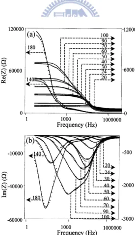
[Fig. 2.20] 2-stack 1D-1R cross-point structure with oxide diodes as switch elements. [Fig. 3.1] The frequency dependences of |Z|, R and X for the PSV at zero field. The resonance frequency (fr) is found at 476 kHz, where X vanishes. The experimental data (open symbols) are very close to the theoretical result (solid curves) calculated from the equivalent circuit shown in the inserted panel.
[Fig. 3.2] (a), and (b) magneto impedance at 100 Hz. At this low frequency, the magneto transport property can be regarded as DC. (c) at resonance frequency fr (476 kHz), MX shape of loop reverse to MR loop. (d) The value of MX is negative at f < fr, and switches to positive at f > fr.
[Fig. 3.3] (a) The frequency dependences of |Z|AP, △Z and MI ratios. (b) The frequency dependences of MR and |MX ratio|.
[Fig. 3.4] The DC MR ratio and resistance (R) of the PSV are functions of the annealing temperature.
[Fig. 3.5] Imaginary part of impedance curves for PSV with different AT temperatures ranging from RT to 200oC.
[Fig. 3.6] The roll-off frequency and effective capacitance of the PSV are functions of the annealing temperature.
[Fig. 3.7] The hysteresis loops of the PSV with AT temperatures RT, 140oC, 160oC,
20 22 22 23 24 27 29 30 32 33 34
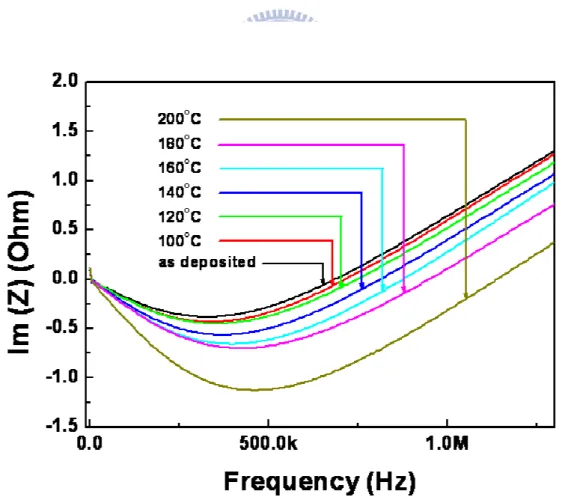
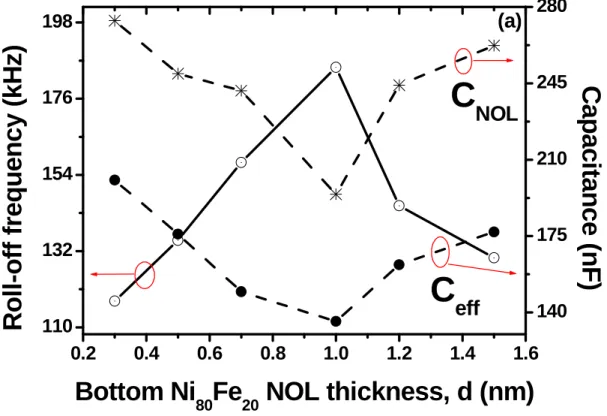
180oC, 200oC, respectively. The inset panels show the equivalent capacitor modes. [Fig. 3.8] The dependences on MR ratio, resistance, and thickness of the bottom Ni80Fe20 in the structure of Ta 0.6 / NOL / Co 3 / Cu 4 / Co 1 / Ni80Fe20 3 / NOL / Ni80Fe20 (d) / substrate, in which the bottom Ni80Fe20 was naturally oxidized for ten minutes. The inset panel shows the magneto impedance at frequency 415 kHz for PSV with d = 1 nm, the shape of MZIm loop is reversed to that of MZRe.
[Fig. 3.9] The imaginary parts of impedance curves for PSV with different thicknesses of the bottom Ni80Fe20 NOL ranged from 0 to 1 nm at zero fields. Except the PSV without Ni80Fe20 NOL, the roll-off frequencies increases as the thickness of the Ni80Fe20 NOL increasing.
[Fig. 3.10] (a) The roll-off frequency and calculated effective and NOL capacitance are functions of the thickness of the bottom Ni80Fe20 NOL thickness. (b) The equivalent circuit of the measurement is a complex RLC combination.
[Fig. 3.11] The imaginary part of impedance curve for PSV with different NOL structures at zero fields. The film structure is Ta / (Co NOL) /Cu /Co /Ni80Fe20 / (Co NOL) /sub.
[Fig. 3.12] The imaginary part of impedance curve for PSV with different NOL structures at zero fields. The film structure is Ta / (Co NOL) /Cu /Co /Ni80Fe20 / (Ta NOL) /sub.
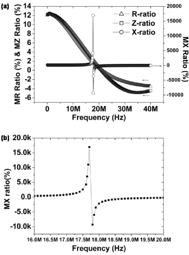
[Fig. 4.1] (a) The structure of the magneto tunneling junctions is Ru (5nm) /Cu (10nm) /Ru(5nm) /IrMn(10nm) /CoFeB(4nm) /Al(1.2nm)-oxide /CoFeB (4nm) /Ru (5nm) and equivalent circuit with contributions from magneto tunneling junctions. [Fig. 4.2] The frequency dependences of the real part of the impedance (R) and the imaginary part of the impedance(X) for the magneto tunneling junctions in the parallel or anti-parallel states. The inset panel shows the crossover frequency of the real part of the impedance, which indicates that the magnetic behavior of MTJ is
34 37 38 39 40 41 45
changed by the driving frequency.
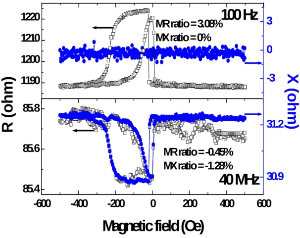
[Fig. 4.3] (a) The real part of the impedance (R) curves at frequencies of 100Hz, 17.7MHz (resonance frequency), 21.1MHz (crossover frequency), and 40MHz for the magneto tunneling junctions. (b) The imaginary part of the impedance (X) curves at frequencies of 100Hz, 17.7MHz (resonance frequency), 21.1MHz (crossover frequency), and 40MHz for the magneto tunneling junctions. (c) The impedance (Z) curves at frequencies of 100Hz, 17.7MHz (resonance frequency), 21.1MHz (crossover frequency), and 40MHz for the magneto tunneling junctions.
[Fig. 4.4] (a) The frequency dependences of MR, MX, and MZ ratios. (b) The zoom in panel of the MX ratio changed; the frequency ranges from 16 to 20 MHz.
[Fig. 4.5] The resistance and capacitance reduced by barrier effect at parallel and anti-parallel states are functions of the oscillating voltage.
[Fig. 4.6] The resistance and capacitance reduced by interface effect at parallel and anti-parallel states are functions of the oscillating voltage.
[Fig. 4.7] The MI ratio of the MTJ with different oscillating voltage ranged from 100Hz to 40 MHz. The inset panel shows the MI ratio at 1MHz and 40MHz.
[Fig. 4.8] It shows the hysteresis behavior of the MTJ Ru(5) /Cu(10) /Ru(5) /IrMn(10) /CoFeB(4) /Al (0.8)-oxide /CoFeB(4) /Ru(5) at frequencies 100Hz, and 40MHz, respectively.
[Fig. 4.9] The frequency dependences of the real part of the impedance (R) and the imaginary part of the impedance (X) for the magneto tunneling junctions in the anti-parallel (a), (b), and parallel states (c), (d).
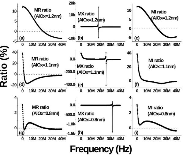
[Fig. 4.10] shows the frequency dependence of the MR, MX, and MI ratio behaviors with different barrier layer AlOx thickness 0.8, 1.1, 1.2nm.
[Fig. 4.11] The resonance frequency (Fr) of the MTJ is a function of the thickness of barrier layer. 47 49 50 52 53 54 56 57 59 60
[Fig. 4.12] The resistance difference between the anti-parallel state and the parallel state (RAP-RP) as a function of the frequency between 100Hz to 40MHz for sample with x = 0.8 nm.
[Fig. 4.13] Simulation results for RAP-RP with different barrier thickness 0.8, 1.1, and 1.2nm at the frequency ranging from 100Hz to 100MHz.
[Fig. 5.1] Cell structure, cross-sectional TEM image and the process flow of the WOX RRAM
[Fig. 5.2] R-V characteristics using fixed pulse width (50ns) before and after forming process. A forming process helps reducing the RESET voltage.
[Fig. 5.3] Hysteresis loop between 3V and –3V with a fixed pulse width of 50ns. The resistance increases gradually and linearly from 1.5V to ~3V, but decreases suddenly at –1.2V.
[Fig. 5.4] Resistance dependence on pulse voltage with fixed pulse width 50ns at 85oC. It again shows a well behaved linear region suitable for MLC programming. [Fig. 5.5] The MLC operation algorithm. Two operation methods may be selected to control the resistance states of the WOx RRAM: (1) varying the pulses voltage, (2) changing the pulse number. R-V plots (Fig. 4) are used to decide the initial parameters. If the resistance does not reach the target value, the programming voltage is increased.
[Fig. 5.6] 4-level cycling test of the WOx RRAM. 1,000 cycles are achieved. 3 RESET states (01,10,11) are programmed by different voltage positive pulses and the SET level (00) is programmed by a negative pulse.
[Fig. 5.7] 100 cells are programmed into 4 levels using the same programming conditions in Fig. 5.6. The levels are well distinguished.
[Fig. 5.8] Cycling test for 8 levels. Although there was no window closing after cycling, the window between adjacent logic levels is too narrow. For 3-bit/cell
61 62 66 67 68 69 69 70 70
operation the total window needs to be further enlarged.
[Fig. 5.9] Read disturb test for WOX RRAM. The states 10, and 11 are not affected by the read bias ranging from 0.2V to 0.6V. The states 00, and 01 are immune to read disturb under 0.4V.
[Fig. 5.10] Device resistance dependence on temperature from 25 to 200oC. The resistances of RESET states 01, 10, and 11 decrease with increasing temperature. The strong temperature dependence may limit application range.
[Fig. 5.11] The log R vs. 1/kBT plot for states 01, 10, and 11. The activation energies are not constant but are similar for all states.
[Fig. 5.12] Resistance stability of the WOX RRAM at room temperature. All 4 states show stable resistance.
[Fig. 5.13] The resistance stability at 85oC. The high resistance states maintain > 1k Ω of window after stressing.
[Fig. 5.14] Thermal stability test for WOX RRAM at 150oC. Each state survives well beyond 106 sec.
[Fig. 5.15] Major processes for self-aligned WOX RRAM: (a) CMP of W plugs, (b) plasma oxidation, (c) photolithography to expose peripheral circuits, (d) remove WOX from W plugs in periphery, (e) top electrode deposition and patterning.
[Fig. 5.16] Cross-sectional TEM for the WOX RRAM cell. HR-TEM (inset) shows that the WOX is amorphous.
[Fig. 5.17] XPS spectra for WOX fabricated by 1600s of oxidation. The film thickness is about 140Å.
[Fig. 5.18] Thickness of WOX film as a function of oxidation time. The film thickness increases slowly after a fast initial growth. However, the film composition varies considerably with the oxidation time.
[Fig. 5.19] Comparison of WOX composition after short (400s) and long (1600s)
71 71 72 73 74 74 75 76 77 77 78
oxidation. The 400s oxidation produces steeply graded WO3 suitable for bipolar switching (Ref. 4). After 1600s of oxidation, the WO3 penetrates through the oxide and film is suitable for unipolar switching (See Fig. 5.21).
[Fig. 5.20] Unipolar switching for fresh devices with various oxidation time. Short oxidation time gives poor unipolar switching capability, while long oxidation time produces films with good unipolar switching property.
[Fig. 5.21] Unipolar switching characteristics of a 1600s device. A short (20-50ns) positive pulse switches the resistivity from LRS to HRS, while long positive pulses (200-500ns) switch the resistivity from HRS back to LRS. Both operations are fully reversible.
[Fig. 5.22] Negative pulses, however, do not produce reversible unipolar switching on 1600s samples. At higher voltages, negative pulses can switch the WOX device from HRS to LRS once, but the device cannot be switched back to HRS anymore. [Fig. 5.23] Temperature dependence of the conduction currents for both the LRS and HRS indicating semiconducting behavior.
[Fig. 5.24] Cycling characteristics of the WOX memory cell. RHS/LHS resistance window keeps well separated up to > 1000 cycles.
[Fig. 5.25] Thermal stability test of WOX memory cell at 1500C. The HRS decreases slowly while the LRS keeps almost constant. A 10X resistivity ratio is maintained up to 2500 hours of baking.
[Fig. 5.26] Read disturb test on WOX devices. The HRS is not affected by the read bias of 0.2-0.6V. LRS is immune to read disturb under bias < 0.4V.
[Fig. 6.1] (a). Cross-sectional TEM image for WOX RRAM. (b) and (c). AFM and Conductive-AFM images of WOX cell surface.
[Fig. 6.2] The resistance state can be enhanced by positive pulse. At high voltage, the device becomes shorted.
78 79 80 81 81 82 83 83 86 88
[Fig. 6.3] Negative pulses, even at higher voltages, do not reset the device.
[Fig. 6.4] R-V characteristics after the forming process. Forming process is useful to reduce the switching voltage.
[Fig. 6.5] The resistance window increases for smaller contact area. The devices are treated with a forming process using a 4V/ 50ns pulse first.
[Fig. 6.6] Voltage distribution for HRS and LRS of 50 memory cells.
[Fig. 6.7] Cycling characteristics of the WOX memory cell. RHS/LHS resistance window is well separated at 50k Ω /10k Ω up to > 108 cycles.
[Fig. 6.8] Time resolved voltage and current traces of RESET operation. The input pulse width is 2ns. The RESET current density is about 3.4x10⁶ A/cm2.
[Fig. 6.9] J-t and V-t curves of SET operation. It also shows high speed erase capability (~2ns). The SET current density is about 3.3x10⁶ A/cm2.
[Fig. 6.10] Transient currents for RESET and SET using various pulse widths. [Fig. 6.11] Corresponding RESET and SET states for various pulse widths.
[Fig. 6.12] 4-level cycling test beyond 104 cycles with verification. Three RESET states (01,10,11) are programmed by different voltage positive pulses and the SET level (00) is programmed by a negative pulse.
[Fig. 6.13] Read disturb test. All states show acceptable read disturb up to 0.5V. [Fig. 6.14] 8-level cycling test of more than 8k cycles with verification. Well distinguishable resistance windows are maintained for each states.
[Fig. 6.15] Schematics for proposed WOX RRAM switching mechanism. (a) Right after the RTO WOX formation and top electrode process, many oxygen vacancies are present in the WOX film leaving easy electron hopping paths. The initial resistance is below 1kΩ due to these conduction paths (sometimes referred to as filaments). (b) During the forming process, the positive voltage drives oxygen into vacancies near the top electrode. This cuts off the conduction paths and the resistance increases
88 89 89 90 91 92 92 93 93 94 95 96
dramatically. (c) When a large enough negative voltage is applied, oxygen is separated from shallow vacancy traps. Thus some of the conduction paths are reconnected and the resistance drops (SET). (d) A positive voltage drives oxygen back into shallow vacancies and disrupt the conduction paths (RESET).
[Fig. 6.16] C-AFM images of the WOX cell surface.
[Fig. 6.17] (a). Unipolar RESET for pulse R-V curves and (b) SET for pulse R-t curves. (c) Pulse width dependence of unipolar SET with varied positive voltage and (d) voltage dependence of unipolar RESET with varied pulse width.
[Fig. 6.18] (a). The IV curves and fitting results for SET and RESET states. (b) Read dependence for RESET and SET states. (c). 1 M read times for 0.25V pulse read voltage.
[Fig. 6.19] (a). Program-verify algorithm for cycling test of RTO WOX RRAM (b). Cycling characteristics of the RTO WOX RRAM cell with unipolar operation. RESET/SET resistance window of 40kΩ/10kΩ is well maintained up to 107 cycles. (c). 4-levels cycling test for 9000 cycles. Three RESET states (01,10,11) are programmed by positive pulses of different voltage and the SET level (00) is programmed by a positive pulse with long pulse width. (d). Retention test for RTO WOX RRAM with 100oC baking. The resistance values are lower indicating the semiconductor behaviors.
[Fig. 6.20] WOX RRAM structure and process flow. [Fig. 6.21] Formulas for SCLC and thermionic emission.
[Fig. 6.22] Fig. 6.20. The initial resistance increases with the WF of the TE. Two types of forming process (I and II) are observed.
[Fig. 6.23] IV curves and fitting results for initial states of Pt/WOX/W, Ni/WOX/W, and TiN/WOX/W. Thermionic emission describes the behaviors for Pt and Ni/WOX/W well, but not TiN TE.
97 98 100 101 102 104 105 105 106
[Fig. 6.24] IV curves and J versus V2 curves for TiN/WOX/W at different temperatures RT, 40, 60, and 80oC. J is proportional to V2 indicating the SCLC behaviors.
[Fig. 6.25] IV curves and thermionic emission fitting results for initial state of Ni/WOX/W at different temperatures RT, 40, 60, and 80
oC.
[Fig. 6.26] IV curves and thermionic emission fitting results for initial state of Pt/WOX/W at different temperatures RT, 40, 60, and 80
oC.
[Fig. 6.27] ln (J/T2) versus 1/kBT curves for Ni/WOX/W and Pt/WOX/W with bias between 0.15V to 0.5V. The linear trend indicates the thermionic emission behaviors [Fig. 6.28] Schematics for conduction mechanism for Pt, Ni, and TiN/WOX/W. [Fig. 6.29] High WF TE produces large resistance window. Both Pt/WOX/W and Ni/WOX/W show 100X window and higher RESET resistance.
[Fig. 6.30] Cross sectional TEM image of Ni/WOX/W RRAM.
[Fig. 6.31] RESET and SET pulse R-V curves for Ni/WOX/W after reverse forming process.
[Fig. 6.32] Transient I-t curves of RESET and SET operation of Ni/WOX/W cell. The RESET current is about 180uA, and SET current is about 150uA.
[Fig. 6.33] Cycling characteristics of the Ni/WOX/W cell. RESET/SET resistance window is well separated at 1MΩ /10kΩ for > 10k cycles.
[Fig. 6.34] Read disturb test. Both RESET and SET states show good read disturb resistance up to 0.6V.
[Fig. 6.35] Thermal stability test for Ni/WOX/W cell at 150 o
C. Both RESET and SET states survive well beyond 106 sec with at least 10X resistance window.
[Fig. 6.36] Arrhenius plot for retention test of Ni/WOX/W cell. Ea is ~ 1.34eV. The reten-tion time is 10years @115oC, and 300 years @ 85oC. The retention criteria is <100kΩ for SET . 107 108 108 109 109 110 111 112 112 113 113 114 114
[Fig. 6.37] Comparison for TiN, Pt, and Ni/WOX/W cells. Ni/WOX/W cell shows promising performance for memory application with low operation current, large
CHAPTER 1
Introduction
1.1 Background and Motivation
Non-volatile memories have drawn much attention in the world. The applications for portable and electronics such as digital still camera (DSC), cellular phone, digital audio machines (MP3 player), memory cards, routers, and so on are indispensable in our life. At the present the electron storage memories like conventional floating gate flash memories, NOR and NAND flash, are popular for non-volatile memory that drive the progress of the world around forty years. Recently, in order to keep corresponding to the market of non-volatile semiconductor memories, owing to its high density and low cost, both for NOR and NAND flash are the most important electronic devices. Up to now, flash memories could scale down to 32nm technology node. However, beyond 32nm technology node, the flash memories face the scaling issues due to physical limitation. Therefore, finding the way to replace the electronic storage memory is a hot and interesting topic for memory research.
Resistive storage memory plays a key role for memory research due to its potential to replace the electronic storage memory. For the purposes of Phase change memory (PCM), magnetic random access memory (MRAM), and resistive random access memory (RRAM) are considered in place of the electronic storage memory because good performance such as high endurance, random access and high operation speed.
MRAM has been developed more than twenty years. This technology always can find new ways to overcome the hinder of technology issues. For instance, the spin transfer torque technique was used to solve the scaling issue for conventional field driven MRAM. Although the operation architecture changes a lot for MRAM evolution, the basic magneto resistive elements are used and dominate the performance of either conventional MRAM or STT
MRAM.
The DC behaviors for magneto resistive elements such as pseudo spin valve (PSV), and magneto tunneling junction (MTJ) have been widely studied, but the AC behaviors are rare. This motivates us to investigate the AC behaviors for PSV and MTJ. In this thesis, the magneto impedance behaviors of the PSV and MTJ are studied. By using the AC analysis, the nano-oxide layer (NOL) effects of PSV could be modeled. Moreover, the equivalent circuit model was used to describe the AC behaviors for the MTJ.
Recently, resistance-based memory has attracted much attention for high-density memory applications because of its simple structure, small cell size, high speed, and low power consumption. Resistance switching memories including transition metal oxides (TMO) and programmable metallization cell (PMC), such as TiOX [72], NiOX [67], MoOX [73], CuOX, TaOX, CoOX [74], and Cu/WOX [75] have been studied extensively. Although a lot of groups devote to study the RRAM for its conducting mechanism, switching mechanism, and device performance, up to now, their switching and conducting mechanisms are still not clear due to the complexity of the many oxides.
Compatibility with the CMOS process is a major criterion in choosing the metal oxide for RRAM design. Tungsten oxide (WOX)-based RRAM is attractive because it requires only one extra mask without contamination issue, new equipment or new material to the standard CMOS process. The device performances of WOX-based RRAM are further studied. The WOX converting by rapid thermal oxidation (RTO) provides the suitable performance such as low switching current, high resistance window, fast programming speed, good thermal stability, and high endurance for nonvolatile memory. Besides the conducting mechanism is also investigated by using different work function electrodes connecting with WOX elements.
1.2 Thesis Organization
This thesis consists seven chapters.
At first, chapter 1 gives a brief introduction and organization for this dissertation. Chapter 2 reviews the previous literatures of emerging resistive memories such as PCM, MRAM, and RRAM.
In chapter 3, the magneto impedance behavior of the PSV is addressed. The NOL effect of the PSV is studied. The new non-destructive analysis method via the magneto impedance spectroscopy for investigate the PSV with different thickness of NOL is provided. Also, the magneto impedance behavior study for MTJ is shown in chapter 4. The equivalent circuit model can well describe the AC phenomenon of the MTJ.
In chapter 5 and 6, the main discussion shifts to RRAM research. The tungsten oxide RRAM by using down stream plasma oxidation (DSPO) is proposed in chapter 5. The device analysis and performance are introduced. Chapter 6 shows the further improved WOX device by using rapid thermal oxidation (RTO) process. The first time transient effect study for WOX device is demonstrated, and it reveals ultra fast program speed for RTO WOX RRAM. Moreover the performance, operation method, and conduction mechanism are explained in detail.
CHAPTER 2
Basic of MRAM and RRAM
2.1 Magnetoresistive Random Access Memory (MRAM)
2.1.1 Magnetoresistance Effect
In this section, we will discussion the magnetoresistance, include pseudo spin valve effect and tunneling magnetoresistance effect.
The pseudo spin valve is composed of a hard magnetic layer, HM, and a soft magnetic layer, SM, magnetically separated with a nonmagnetic layer, NM. The HM has a larger coercivity than the SM. A prototype pseudo spin valve film proposed by Shinjo et al. is [NiFe(3)/Cu(5)/Co(3)/Cu(5)]15 multilayered film [1]. NiFe is used for the SM and Co is used for the HM. This multilayered film showed a MR ratio of ~8%. The magnetocrystalline anisotropy energy, Ea, for the films having cubic symmetry is given as
Ea=K1/8(1-cos4θ)+…
Fig. 2.1. (a) Magnetization curve and (b) MR curve of the pseudo-spin-valve, where the magnetization directions of the SM and the HM are denoted with gray and black arrows, respectively.
When the magnetization rotates in the (100) plane, where θ is the angle between the magnetization direction and the [010] axis. The K1 is the negative for fcc NiFe and Co. Therefore, the NiFe and Co layers have the easy axis along the [011] direction. This is the reason why the magnetization reversal of the NiFe and Co layers take place. These characteristics are suitable for the application of pseudo-spin-valve to MRAM devices, as the magnetization reversal of the HM(=Co) layers is used for the data writing and that of SM(=NiFe) layers is used for data reading, The switching field of SM is lower than that of the HM layers. The schematic magnetization curve and the MR curve of the pseudo-spin-valve are shown in Fig. 2.1(a) and (b). With the application of a small magnetic field that causes magnetization reversal of the SM, but not of the HM, the magnetization directions of the SM and the HM take an antiparallel configuration. Then, the pseudo-spin-valve shows high resistance. With the application of a large magnetic field that causes magnetization reversal of the HM, the magnetization directions of the SM and HM take a parallel configuration and the pseudo-spin-valve shows low resistance. Pseudo-spin-valve shows a symmetric MR curve with the magnetic field direction, while the exchange-biased spin valves show a nonsymmetric one as shown in Fig. 2.2, as the HM in the pseudo-spin-valve has uniaxial anisotropy, while the pinned magnetic layer (PL)/ antiferromagnetic (AF) in the exchange-bias spin valve has unidirectional anisotropy.
Fig. 2.2. MR curve for the single spin valve, where the magnetization directions of the FM and the PL are denoted with gray and black arrows, respectively.
The exchange-biased spin valve shows a reversible MR curve with the magnetic field. But the pseudo-spin-valve shows an irreversible one. This is a disadvantage of pseudo-spin-valve for application to MR heads. However, pseudo-spin-valves are studied for application to MRAM (magnetic random access memory) devices [2,3].
Tunneling magnetoresistance (TMR) is observed for ferromagnetic spin tunneling junctions (MTJ) consisting of ferromagnetic-insulator- ferromagnetic layers [4-6]. When the insulating layer, usually referred to as the barrier layer, is very thin (the order of 1nm), electrons can tunnel through this forbidden region as a result of the wave-like nature of electrons for a voltage applied between the two electrodes, and can only be described in terms of quantum mechanics. The basic principle of TMR is the dependence of the tunneling probability on the relative orientation of magnetization in the two ferromagnetic electrodes. The tunneling conductance is spin dependent due to the spin dependent density of states (DOS) at the Fermi level for ferromagnets. When the applied voltage is small enough for electrons near the Fermi level to tunnel, the tunneling conductance G in the MTJ can be written as (2.1.1)-(2.1.2) by neglecting the spin dependency of the tunneling probability [7],
( ) ( )
∑
= = − F F D E E D T R G 1 σ 2 1σ 2σ ………....(2.1.1)(
sχ)
T 2exp−2 ………..……(2.1.2)(
)
[
2 2]
/ 8 m× −EF h =π
ϕ
χ
………...(2.1.3)where R, T, Diσ(EF) are the junction resistance, tunneling probability, DOS at the Fermi level for spin σ band of the i-th ferromagnet, respectively, andφ,s, χand h are the barrier height and thickness, electron wave vector in the barrier and the Planck constant, respectively. The TMR is defined as
(
RAP RP)
RPTMR= − / ………..…………(2.1.4)
where RP and RAP are the resistance for parallel and antiparallel spin configurations of two ferromagnetic electrodes, respectively. If we assume that spin is conserved during tunneling as shown Fig. 2.3, (2.1.1)-(2.1.4) lead to Julliere’s model [4],
(
1 2)
2 1 /1
2PP PP
Fig. 2.3. A schematic model for spin dependent tunneling
Fig. 2.4. Probing the spin polarization of tunneling electrons from the ferromagnet to the superconductor
Pi is the spin polarization of tunneling electrons of ferromagnet i and given by
(
↑ − ↓) (
↑ + ↓)
= i i i i
i D D D D
P / ………..(2.1.6)
TMR can vary over a wide range depending on the P values of ferromagnets as verified by (2.1.5) and (2.1.6). For vanishing polarization of one of the electrodes the magnetoresistance disappears, while for full polarization of the tunneling electrons of both electrodes (P1=P2=1) the effect will become infinitely large corresponding to a value of 1 in (2.1.5). Unfortunately, determining the spin polarization at the Fermi energy of a ferromagnet is not easy. A typical transition metal ferromagnet has two components to its electronic structure; narrow d-bands that may be fully or partially spin polarized and broad s-bands with a lesser degree of spin polarization due to hybridization with the d-bonds. The value of P is controlled by extending to which these s- and d-bonds cross the Fermi energy. If the orbital character at the Fermi surface of the ferromagnetic metal is primarily d-like, then the spin polarization will be high. If the orbital character, however, is s-like or s-d hybridized, then the spin polarization can be low or high depending on the detail of the electronic structure. The magnetization of a material may show that all the electronic spins associated with the d orbits are aligned but the spin polarization at EF can de depressed. On the other hand, metallic oxide ferromagnets, for example, have a greater opportunity for high spin polarization because of the predominance of the d orbital character at EF.
Measuring the spin polarization requires a spectroscopic technique that can discriminate between the spin-up and spin-down electrons near EF spin polarized photoemission spectroscopy is technically capable of providing the most direct measurement of P, but lacks the necessary energy resolution (~1meV). An effective alternative to photoemission is the use of spin polarized tunneling in a planar junction geometry which does allow the electronic spectrum near EF to be probe with sub-meV energy resolution.
Tedrow and Meservey pioneered this technique by marking superconductor/insulator/ferromagnet junctions and Zeeman splitting the superconductor’s strongly peaked single-particle excitation spectrum by the application of a magnetic field [8]. The spin-splitting of the quasiparticle density of states in a superconductor by the application of a magnetic field allows probing the spin polarization of tunneling electrons from the ferromagnet, which is schematically shown in Fig. 2.4. The resulting spectrum of the superconductor roughly corresponds to two fully spin polarized peaks (neglecting spin-orbit
coupling effects) that can be used to detect the spin polarization of a current from the ferromagnetic film. Another method of measuring spin polarization of a metal was developed recently [9], which is a metallic point contact between the point contact measures the conversion between superconducting pairs and the single particle charge carriers of the metal. The conversion of normal current to supercurrent at a metallic interface is called Andreev reflection.
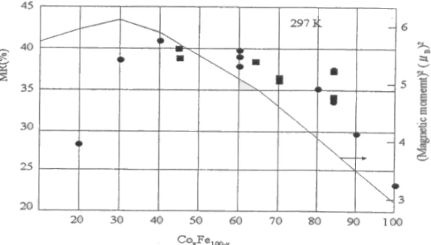
The values of P measured are shown in Table 2.1.1 for various ferromagnets except for the theoretically expected values for half metals with P=1, which have an energy gap in the minority spin (down spin) band as shown schematically in Fig. 2.5, thus only majority spin (up spin) electrons at the Fermi level. The spin polarization of tunneling electrons seems to be nearly proportional to the magnetic moment µ of the electrode as shown for Ni-Fe alloys in Fig. 2.6 [8], while it is not always proportional to µ of the ferromagnetic electrode as shown in Fig. 2.7 [10], which exhibits TMR and µ2 as a function of the composition of Fe-Co alloy electrodes used for the junctions.
Table 2.1.1 Spin polarization of various magnetic materials
Magnetic material Spin polarization Magnetic materials Spin polarization
Fe 0.44 NiMnSb 1,0.58
Co 0.35 PtMnSb 1
Ni 0.23 CrO2 1
Ni80Fe20 0.25,0.45 Fe3O4 1
Fe50Co50 0.53 (La-Sr)MnO3 1
Equation (2.1.5) assumes that all electrons at the Fermi level have the same probability of tunneling and also neglects the influence of the barrier. In fact, however, TMR depends on tunneling barrier height for the MTJ using CoFe electrodes. The TMR is larger for the higher barrier height. The barrier height can be estimated by Simmons’ expressions (2.1.7)-(2.1.10)
(
3)
, V V J =β
+ ………(2.1.7)(
)
[
3 2 2 1/2/2 2]
exp(
1/2)
[
1 2]
, cm A s h m e − Ω− = φ φ β ………..(2.1.8)( )
2/96φ 2/32φ1/4, γ = Ae −Ae ………(2.1.9)( )
2 / 1.02 /( )
, 4 1/2 1/2 = = m s h A eVo Aπ
……….(2.1.10)for lower bias voltage, where J, φ and s are current density [A/cm2], barrier height [eV] and barrier thickness [cm], respectively.
Fig. 2.5. Schematic energy band structure for a half metal
Fig. 2.6. Spin polarization of tunneling electrons versus the magnetic moment µ of the electrode.
Fig. 2.7. TMR and µ2 as function of the composition of Fe-Co alloy electrodes used for the junctions.
2.1.2 Magneto Impedance Theory
Magneto impedance, MI = M|Z|eiθ = MR +iMX, in which X = XL-XC, originates mainly from the inductance and capacitance of the magneto device. Z is the impedance, θ is the phase angle, R is the real part of magneto impedance, and X is the imaginary part of magneto impedance.
In 1999, X.Q. Xiao [11] shows giant magnetoimpedance (GMI) effect in films with a sandwiched structure [12]. As compared to single layered films, the sandwiched films have much higher GMI ratio at relatively low frequencies. This is because of the separation of the ac current path from the magnetic flux path. The inner highly conductive metal reduces the entire resistance of the sandwiched film, and the outer magnetic layers form a magnetic alloy closed-loop structure. Therefore, less power is dissipated in the films to generate the ac transverse field. In the FeNiCrSiB/Cu/FeNiCrSiB structure, GMI ratios of 63% and 77% have been obtained at 13 MHz in longitudinal and transverse fields, respectively as shown in Fig. 2.8. These values are almost twice as large as those obtained in single layered FeNiCrSiB films.
Fig. 2.8. Field dependence of △∣Z∣/∣Zs∣ at 13 MHz in longitudinal (filled symbols) and transverse (hollowed symbols) field.
In 2000, M.F. Gillies [13] further proposed the magneto impedance effect for magneto tunneling junctions [14]. The structure is the Si/SiO2/Co/AlOx /Co. Due to differing conductivities charge collects at the interface between the dielectrics as well as on the capacitor plates (Maxwell Wagner capacitor model). This results in two contributions to the impedance. In the case of the magnetic tunnel junctions studied, they extend this simple analysis to more than two layers in order to provide a model with which the complicated results of the impedance measurements as shown in Fig. 2.9 (a) and (b). By this AC analysis, the oxide/Co multilayer proved a very useful way of determining the total oxide thickness as a function of oxidation time and allowed a rough check of what was determined from the impedance measurements. The strength of the impedance measurements is that they provide a “fingerprint'' of the oxide, rather than definitive fit parameters, and in so doing help to characterize the oxide.
Fig. 2.9. (a) Real and (b) imaginary parts of impedance for junctions with different oxidation times (in seconds). In both figures the dots show the measured results and the solid lines are fits.
2.1.3 Field Driven Magnetization Switching Designs
In most of today’s MRAM designs, the memory element is a magnetic tunnel junction (MTJ) that consists of two magnetic electrodes sandwiching an insulative tunnel barrier, as shown in Fig. 2.10 [15-18]. The resistance of these magnetic tunnel junctions depends on the relative orientation of the magnetic moments in the two magnetic electrodes interfacing with the tunnel barrier [19-22]. When the magnetic moments of the two magnetic layers are antiparallel, the resistance of the tunnel junction is significantly higher than when they are in parallel. The magnetic electrodes are shaped like an ellipse to create a shape-defined magnetic anisotropy. The magnetic moment will always be resting along the long axis of the element, referred to as the magnetic easy axis, as shown in Fig. 2.11 [23]. Assuming we can “fix” or “pin” the direction of the magnetic moment of the bottom layer, referred to as the reference layer, along the easy axis, the magnetic moment orientation of the storage layer along the easy axis will give rise to two states with distinctively different resistance values, thereby, the two states in binary bit. The magnetization of the reference layer is “fixed” via a multilayer structure, which includes an antiferromagnetic layer at the bottom. The reference layer is part of a trilayer known as synthetic antiferromagnet (SAF) that is free of stray field. A good example is CoFe/Ru/CoFe with Ru of thickness around 8A˚. The antiferromagnetic layer yields an interfacial exchange field that “pins” the magnetic moment of the bottom SAF layer (pinned layer).
In a memory element array, each memory element is connected to a transistor, which performs the read addressing for reading back the memory state of an individual cell. The memory state writing of an individual memory element in the array is performed by a x-y grid of conducting wires, referred to as word lines and digital lines, placed over and below the memory elements with a memory element located at each cross, as shown in Fig. 2.12.
A current flowing through a selected word line (running in the y-direction in the figure) generates a magnetic field along the easy axis Hx while a current flowing through a selected
digital line (running in the x-direction) generates a field Hy in a direction transverse to the easy axis. A simple theoretical analysis shows that the field threshold for resulting in a magnetic switching is given by Hx2/3+Hy2/3=Hk2/3 often referred to as the Stoner–Wohlfarth switching astroid, where Hk is the anisotropy field of the element [24]. According to the above equation, the switching field threshold is the lowest when both field components are equal in magnitude: The memory state of the element at the cross of the activated word line and digital line can be changed. Whereas the rest of the elements along the selected word or digital lines, known as the half-selected elements, shall not be affected since they only experience one of the two fields, provided each field component is below Hk.
Fig. 2.10. Schematic drawing of a typical magnetic tunnel junction memory element and corresponding memory states that have two distinctive resistance values due to the magnetoresistive effect.
Fig. 2.11. Simulated magnetic switching of an eye-shaped magnetic element. The magnetization reversal starts at the center of the element with quasi-coherent magnetization rotation. The reversed region expands towards the ends as the reversal completes.
Fig. 2.12. Schematic drawing of the memory element array. Each memory element is connected to a field effect transistor for read addressing. A grid of x-y conducting wires, known as the digital lines (wires along the x-direction) and word lines (wires along the y-direction), is placed over and below the memory elements for providing the magnetic field for the write operation. Each memory element is located at a cross in the x-y wire grid. The lower bottom shows the switching field threshold contour, known as the Stoner–Wohlfarth switching astroid. The magnetization of the storage layer will remain unchanged if the field applied is located within the enclosed region of the astroid. Otherwise, the magnetic moment will irreversibly switch to the direction of the word line field.
2.1.4 Spin Torque Transfer Driven Switching Designs
Right before the turn of the century, researchers demonstrated magnetic switching of a patterned magnetic element at deep submicrometer dimension by direct perpendicular current injection [25-28], a phenomenon previously predicted by theorists Berger and Slonczewski, known as spin torque transfer [29,30]. When current is injected normally through a uniformly and firmly magnetized ferromagnetic layer, i.e., the reference layer, acts as a “spin filter”: the injected electrons with spin parallel to the magnetization direction of the ferromagnetic layer get transmitted and the electrons with antiparallel spins get, partially, reflected. The current becomes spin polarized in the vicinity of the reference layer. If another magnetic layer, i.e., the free layer, is placed within the range of the spin polarization, the spin polarized current would result in a torque, referred to as spin torque that is, to rotate the local magnetic moment away from the equilibrium orientation direction causing the magnetic moment to precess around the local effective magnetic field. This spin torque will be present until the local magnetization becomes parallel to the spin polarization direction. The current spin polarization is opposite in sign at the opposite side of the reference layer with respect to the direction of injection. Reversing current direction, thus, reverses the sign of the spin torque, as illustrated in Fig.2.13. If the spin torque, proportional to the injected current density, in the free layer exceeds the restrain torque caused by local magnetic anisotropy, magnetization rotation occurs. The critical current density to irreversibly reverse the magnetic moment of the free layer is given by the following [20]:
where MS, tF, and Hk are the saturation magnetization, the thickness, and the anisotropy field of the free layer, respectively. Also in the above equation, α, known as the Gilbert damping constant, is a phenomenological parameter measuring the magnitude of the damping torque that yields a natural dissipation of the magnetic energy into other nonmagnetic energy form(s),
Fig. 2.13. Illustration of spin torque transfer. Injecting a current through a ferromagnetic layer of a ‘‘fixed’’ magnetization, the current will be spin polarized. Placing a free layer nearby, the spin polarized current will result in a torque that will act to rotate free-layer magnetization away from the equilibrium orientation. The sign of spin polarization direction outside of the ‘‘fix’’ layer reverses with reversing direction of current.
such as heat. The most commonly recognized energy dissipation channel is the coupling between spin waves and lattice vibration, known as magnon–phonon interaction. With a slight manipulation, above equation can be rewritten as
where A, V, and Ku are the surface area, the volume, and the anisotropy energy constant of a free layer, respectively, and IC0 is the critical current amplitude. The term KuV on the right-hand side is the anisotropy energy of the free layer, namely, the magnetic energy stored in the memory element or the energy barrier between the two memory states. It is important to note that the volume V in the above equation should be the activation volume, which could be smaller than the actual volume of a memory element. The term arises from the surface demagnetizing energy due to the out-of-plane precession of the magnetization during the switching. It is important to note that the surface demagnetizing energy is typically greater than the energy stored in the bit. The fact that the Gilbert damping constant appears in above equation reflects the nature of spin torque transfer driven magnetization reversal.
In a free layer at equilibrium absent spin torque transfer, the magnetization is always parallel to the local effective magnetic field, a direct result of the existed damping torque due to energy dissipation. When free-layer magnetization is in the opposite direction of the current spin polarization, the spin torque is effectively antidamping: its direction is exactly opposite to that of the damping torque. When the magnitude of spin torque becomes greater than that of the damping torque, the energy of the local magnetic moment increases with time and an irreversible magnetization reversal could eventually occur. A smaller damping torque will yield a smaller critical current for irreversible magnetization reversal. When the energy barrier between the two memory states becomes comparable to the thermal activation energy, kT where k is the Boltzmann constant and T is the absolute temperature, memory state switching can occur at a current level below switching threshold, as illustrated in Fig.2.14. The probability per unit time for a transition between the memory states to occur is given as
where f0 is known as the attempt frequency and its value is believed to be on the order of 109 to 1010 Hz. With an injected current pulse at a density and a pulse duration, the memory state switching probability is [31.32]
The above relationship is often used for quantitative determination of the energy barrier [32]. Fig. 2.15 shows a schematic view of a typical STT-MRAM memory cell along with a representative example of a magnetic memory element stack [33,34]. For switching the memory state of an element with 50nm/100nm for short/long axes, the injected current pulse is typically 200 µA in amplitude and 5 ns in duration, corresponding to a switching energy on the order of a few pJ. Compared to the toggle MRAM, whose switching energy per bit is on the order of 100 pJ, the energy consumption is substantially reduced. The STT-driven
magnetization reversal offers a means to switch the magnetic state of the storage layer by directly injecting current through the memory element, hence eliminating the x-y grid of write lines and half-select problem discussion in previous sections.
In addition, the spin torque transfer is significantly more efficient in terms of switching free-layer magnetic moment for elements in deep submicrometer dimensions or below. Therefore, it could be the dream memory since it has the potential to replace all the existing memory devices in a computer, maybe even the hard disk drives, becoming the “universal memory”.
Fig. 2.14. Illustration of (a) thermally excited magnetization switching and (b) thermally assisted magnetization switching in which the energy barrier is lowered due to the presence of either a magnetic field or a spin torque transfer by injected spin polarized current.
Fig. 2.15. Illustration of a spin torque transfer MRAM memory cell. (a) Schematic view and (b) illustration of the memory cell with addressing transistor on a Si wafer.
2.2 Resistive Random Access Memory (RRAM)
Starting in the 1960s, a huge variety of materials in an MIM configuration have been reported to show hysteretic resistance switching, with a first period of high research activity until the mid-1980s. A second, on-going period started in the late-1990s, triggered by Asamitsu et al. [35], Kozicki et al. [36] and Beck et al. [37], recently reviewed [38,39].
2.2.1 Unipolar and Bipolar Behaviors
In general, two switching schemes need to be distinguished. Switching is called unipolar (or: symmetric) when the switching procedure does not depend on the polarity of the voltage and current signal (Fig. 2.16a). In contrast, the characteristic is called bipolar (or: antisymmetric) when the set to an ON-state occurs at one voltage polarity and the reset to the OFF-state on reversed voltage polarity (Fig. 2.16b). In both characteristics, unipolar and bipolar, reading of the state is conducted at small voltages, which do not affect the state.
Fig. 2.16. Unipolar and bipolar switching schemes. CC denotes the compliance current, often needed to limit the ON current
(a)
2.2.2 Electrochemical Metallization Effect
One class within this category relies on an electrochemically active electrode metal such as Ag, the drift of the highly mobile Ag+ cations in the ion conducting layer, their discharge at the (inert) counterelectrode leading to a growth of Ag dendrites which form a highly conductive filament in the ON state of the cell [40]. Upon reversal of polarity of the applied voltage, an electrochemical dissolution of the conductive bridges takes place, resetting the system into the OFF state (Fig. 2.17). The redox reactions for Ag2S as an Ag ion conductor read as:
The asymmetry of the OFF switching has been a matter of some debate, because it appeared to be unclear why the “opening” of the Ag bridge should occur at a different voltage polarity than the “closing”. Using a model system with an aqueous electrolyte we have recently been able to demonstrate that the asymmetry arises from the morphology, i. e. the needle-to-plane geometry of the configuration as shown by electrochemical simulations (Fig. 2.18) [41].
2.2.3 Valency Change Switching Effect
In many transition metal oxides, oxygen ions defects, typically oxygen vacancies, are much more mobile than cations. If the cathode blocks ion exchange reactions during an electroforming process, an oxygen deficient region starts to build and to expand towards the anode. Transition metal cations accommodate this deficiency by trapping electrons emitted from the cathode. In the case of TiO2 or titanates, for example, this reduction reaction
…
Fig. 2.17. Sketch of a resistive switching effect based on the electrochemical metallization process.
Fig. 2.18. Field simulation of the front-most Ag dendrite and the Ag electrode; (a) late ON state; (b) early OFF state.
is equivalent to filling the Ti 3d band. The reduced valency states of the transition metal cations which are generated by this electrochemical process typically turn the oxide into a metallically conducting phase, such as, e. g., TiO2-n/2 for approx. n>1.5. This “virtual cathode” moves towards the anode and will finally form a conductive path [42]. At the anode, the oxidation reaction may lead to the evolution of oxygen gas. As an alternative, material of or nearby the anode may be oxidized. Once the electroforming is completed, the bipolar switching obviously takes place through local redox reactions between the virtual cathode and the anode, i. e. by forming or breaking the conductive contact (Fig. 2.19).
Fig. 2.19. I-V measurement of a 100 x 100 nm² Pt/TiO2/Ti/Pt resistive switching cell. The SEM picture shows the single cell in cross junction configuration (C. Kügeler et al., unpublished data).