參材質/雙材質具氧化層基體絕緣結構之三閘極金氧半場效電晶體含氧化層介面缺陷電荷之次臨界行為研究
255
0
0
全文
(2)
(3) 參材質/雙材質具氧化層基體絕緣結構之三閘極金氧半 場效電晶體含氧化層介面缺陷電荷之次臨界行為研究. 指導教授:江德光 博士 國立高雄大學電機工程系 電機工程研究所 學生:張鐸瀚 國立高雄大學電機工程系 電機工程研究所 摘要 依據 ITRS2009(International Technology of Roadmap for Semiconductor)報告,傳統 平面電晶體(Planar Transistor)由於欠缺完好之短通道之控制特性,已無法因應未來高堆 疊密度電路所需微小元件之要求,取而代之,為具良好短通道之控制行為與高堆疊密 度之立體元件如雙閘極電晶體(Double-Gate MOSFET)、三閘極電晶體(Triple-Gate MOSFET)、四閘極電晶體(Four-Gate MOSFET)與環繞閘極電晶體(Surrounding-Gate MOSFET)。過去數十年來,雖然有研究關於平面單閘極電晶體與雙閘極電晶體之次臨 界行為,但截至目前為止,相關之研究有關立體元件三閘極電晶體含氧化層缺陷介面 電荷次臨界電特性仍相當欠缺,而針對植入帶電電荷改變電特性之記憶體元件(Charge Trapped or Injection Memory Device)應用而言,實有必要研究其次臨界行為特性與表面 缺陷電荷之關係,並推導出可用之元件模型,以期該元件將來被有效應用於記憶體電 路中。 本論文乃基於帕森方程式之全二維解與全三維解,成功地推導出三閘極電晶體具 氧化層基體絕緣結構之次臨界行為解析模型,此模型不僅準確顯示出電位分佈 (potential distribution) 、電場分佈(electric field distribution) 、次臨界斜率(subthreshold slope) 、 次 臨 界 電 流 (subthreshold current) 、 和 臨 界 電 壓 縮 減 (threshold voltage degradation)、汲極偏壓導致能障降低(drain-induced-barrier-lowering, DIBL)等效應,而 且此模型之演算結果與模擬數據相當接近,足以提供基本元件設計之導向,並進而被 應用於積體電路設計之模擬。. 關鍵字:雙材質三閘極金氧半場效電晶體、參材質三閘極金氧半場效電晶體、氧化層 缺陷介面電荷、短通道行為、短通道臨界電壓縮減 i.
(4) The Investigation on Subthreshold Behavior Model for the Tri-Material/Dual-Material SOI Triple-Gate MOSFETs with/without the Localized Interface Trapped Charges Advisor: Dr. TE-KUANG CHIANG Department of Electrical Engineering, Institute of Electrical Engineering, National University of Kaohsiung Student: DUO-HAN CHANG Department of Electrical Engineering, Institute of Electrical Engineering, National University of Kaohsiung ABSTRACT ITRS2009 (International Technology of Roadmap for Semiconductor) has revealed that the conventional planar transistor is a lack of well-controlled short-channel effects and high packing density. With the strong field confinement, prominent volume conduction, and high packing density, the triple-gate MOSFETs that have demonstrated improved short-channel immunity and high driving currents can be the promising candidates for memory cells. A numerous of literatures have modeled the hot-carrier-induced threshold voltage of planar and double-gate MOSFETs in the past decade. Until now, there is no literature to investigate the subthreshold behavior model of the triple-gate MOSFETs with/without the localized interface trapped charges. With the application for Charge Trapped or Injection Memory Device, we report the 2D/3D analytical model of the subthreshold behavior for the triple-gate MOSFETs. In this thesis, based on the exact solution of the Poisson equation and perimeterweighted-sum approach, an analytical subthreshold model for the triple-gate MOSFETs with/without localized interface trapped charges is developed by considering the effects of equivalent oxide charges on the flat-band voltage. The model explicitly shows the potential distribution, the electric field distribution, subthreshold slope, subthreshold current, threshold voltage roll-off, and drain-induced-barrier-lowing (DIBL) effect. The model is verified by the 2D/3D device simulator and can be efficiently used to investigate the hot-carrier-induced threshold voltage degradation of the advanced triple-gate MOSFETs charge-trapped memory device. This model not only gives the physical insights into the device physics but also offers the basic designing guidance of the SOI triple-gate transistor. Due to its computational efficiency, this model can be applied for SPICE simulation. Keywords : Tri-Material/Dual-Material Triple-Gate MOSFETs, Localized Interface Trapped Charges, Short-Channel Effect, Threshold Voltage Degradation ii.
(5) Acknowledgements I would like to express my sincerest and utmost gratitude to my advisor, Prof. T.K. Chiang for his full support and his incredible patience. I never thought this complicated thesis would be finished until the very last minute. Honestly, I have suffered so much misery during the lengthy process of writing this thesis. His inspiring encouragement and cordial persistence gave me strength whenever I was in despair. He has spent so much time helping me clarify my thoughts when I encountered confusion. His valuable and insightful review provided constructive feedback to my drafts. I really appreciate his dedication to this thesis. Further, my special appreciation also goes to the committee members of our research group, M.J. Yang, C.F. Lai, H.K. Wang, P.H. Chen, and C.W. Liu for their cooperation and their time devotion on listening to my presentation. Without the support and assistance from everyone mentioned above, it would not be possible for me to finish the research. Finally, I would deliver my enormous thankfulness to my family for their concern and endless love during these years. They encouraged me to pursue master degree and offered me the opportunity to do this research without financial pressure. Meanwhile, I also feel sorry to them for my being engrossed in this thesis without taking care of them much. To reciprocate their love and support, I was determined to move heaven and earth to finish this thesis. Another important person to the completion of this thesis goes to my girl friend, C.Y. Shih who volunteered to check my writing and revised spelling or grammatical errors. I appreciate her efforts very much. Last but not least, I especially would like to extend my appreciation to Prof. Y.H. Wang and Prof. J.T. Lin for being our oral defense committee members. Their presence is really an honor to our research group. Now that I have found the gold mine, I would keep excavating it and make the most of it. It seems this thesis comes to the end. Actually, it is just the preliminary of my exploration.. iii.
(6) Contents 摘要. i. Abstract. ii. Acknowledgements. iii. Contents. iv viii. List of Figures. Chapter 11 Introduction .....................................................................................................1 1.11 . 1Motive of the Thesis.....................................................................................1 1.21 . 1Tri-Gate Device Overview...........................................................................4 Chapter 21 Two Dimensional Subthreshold Behavior Model for SOI Tri-Gate MOSFETs........................................................................................................6 2.11 . 1Two Dimensional Subthreshold Behavior Model for SOI Single-Gate MOSFETs ....................................................................................................6 2.1.1. Model Derivation .........................................................................................6. 2.1.2. 2-D Boundary Conditions Value Problem ...................................................8. 2.1.3. 1-D Solution...............................................................................................10. 2.1.4. Scaling Length ...........................................................................................11. 2.1.5. Coefficients Solution .................................................................................13. 2.1.6. 2-D Generalized Potential Model ..............................................................15. 2.1.7. Potential Contour .......................................................................................18. 2.1.8. Minimum Surface Potential .......................................................................20. 2.1.9. Threshold Voltage Roll-off Model .............................................................22. 2.1.10TSubthreshold Slope Model ........................................................................28 2.2.1. Two Dimensional Subthreshold Behavior Model for Double-Gate MOSFETs ..................................................................................................31. 2.2.1. Model Derivation .......................................................................................31. 2.2.2. 2-D Boundary Conditions Value Problem .................................................33. 2.2.3. 1-D Solution...............................................................................................34. 2.2.4. Scaling Length ...........................................................................................35. 2.2.5. Coefficients Solution .................................................................................37 iv.
(7) 2.2.6. 2-D Generalized Potential Model ..............................................................39. 2.2.7. Potential Contour .......................................................................................42. 2.2.8. Minimum Surface Potential .......................................................................44. 2.2.9. Threshold Voltage Roll-off Model .............................................................46. 2.2.10TSubthreshold Slope Model ........................................................................51 2.3.1. Two Dimensional Subthreshold Behavior Model for SOI Tri-Gate MOSFETs ..................................................................................................54. 2.3.1. Model Derivation .......................................................................................54. 2.3.2. 3-D Generalized Potential Model ..............................................................56. 2.3.3. Potential Contour .......................................................................................60. 2.3.4. Minimum Channel Potential ......................................................................62. 2.3.5. Threshold Voltage Roll-off Model .............................................................64. 2.3.6. Subthreshold Slope Model.........................................................................68. 2.4.1. Results and Discussion ..............................................................................71. Chapter 31 Two Dimensional Subthreshold Behavior Model for SOI Tri-Material Tri-Gate (TMTG) MOSFETs ........................................................................72 3.1.1. Two Dimensional Subthreshold Behavior Model for SOI Tri-Material Single-Gate MOSFETs ..............................................................................72. 3.1.1. Model Derivation .......................................................................................72. 3.1.2. 2-D Boundary Conditions Value Problem .................................................74. 3.1.3. 1-D Solution...............................................................................................76. 3.1.4. Scaling Length ...........................................................................................77. 3.1.5. Coefficients Solution .................................................................................79. 3.1.6. 2-D Generalized Potential Model ..............................................................80. 3.1.7. Minimum Channel Potential ......................................................................84. 3.1.8. Electric Field..............................................................................................86. 3.1.9. Threshold Voltage Roll-off Model .............................................................88. 3.1.10TSubthreshold Slope Model ........................................................................95 3.1.11TSubthreshold Current Model .....................................................................99 3.2.1. Two Dimensional Subthreshold Behavior Model for Tri-Material Double-Gate (TMDG) MOSFETs ...........................................................103. 3.2.1. Model Derivation .....................................................................................103. 3.2.2. 2-D Boundary Conditions Value Problem ...............................................105 v.
(8) 3.2.3. 1-D Solution.............................................................................................107. 3.2.4. Scaling Length .........................................................................................108. 3.2.5. Coefficients Solution ...............................................................................110. 3.2.6. 2-D Generalized Potential Model ............................................................111. 3.2.7. Minimum Channel Potential ....................................................................115. 3.2.8. Electric Field............................................................................................117. 3.2.9. Threshold Voltage Roll-off Model ...........................................................119. 3.2.10TSubthreshold Slope Model ......................................................................126 3.2.11TSubthreshold Current Model ...................................................................130 3.3.1. Two Dimensional Subthreshold Behavior Model for SOI Tri-Material Tri-Gate (TMTG) MOSFETs...................................................................135. 3.3.1. Model Derivation .....................................................................................135. 3.3.2. 3-D Generalized Potential Model ............................................................137. 3.3.3. Minimum Channel Potential ....................................................................144. 3.3.4. Electric Field and Potential Contour........................................................146. 3.3.5. Threshold Voltage Roll-off Model ...........................................................149. 3.3.6. Subthreshold Slope Model.......................................................................153. 3.3.7. Subthreshold Current Model....................................................................157. 3.4.1. Results and Discussion ............................................................................160. Chapter 41 Two Dimensional Model for Tri-Gate MOSFETs with Localized Trapped Chapter 41 Charges........................................................................................................162 4.1. Introduction.................................................................................................162. 4.2. Model Description ......................................................................................164. 4.3. 2-D Generalized Potential Model ...............................................................165. 4.4. Threshold Voltage Model............................................................................171. 4.5. Results and Discussion ...............................................................................177. Chapter 51 Three Dimensional Subthreshold Behavior Model for Dual-Material Chapter 51 Tri-Gate (DMTG) SOI MOSFETs ..............................................................178 5.1. Model Derivation ........................................................................................178. 5.2. 3-D Boundary Conditions Value Problem ..................................................181. 5.3. 1-D Solution................................................................................................184. 5.4. 2-D Coefficients Solution ...........................................................................186. 5.5. 3-D Laplace Equation Solution...................................................................189 vi.
(9) 5.6. 3-D Generalized Potential Model ...............................................................194. 5.7. Minimum Channel Potential .......................................................................203. 5.8 Electric Field and Potential Contour...........................................................205 5.9. Threshold Voltage Roll-off Model ..............................................................209. 5.10TSubthreshold Slope Model .........................................................................216 5.11TSubthreshold Current Model ......................................................................221 5.12TResults and Discussion ...............................................................................225 Chapter 61 Conclusions and Future Works....................................................................226 6.1. Conclusions.................................................................................................226. 6.2. Future Works...............................................................................................226. References......................................................................................................................227. PUBLICATION LIST. 233. VITA. 234. vii.
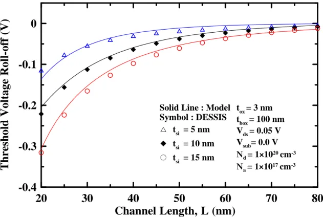
(10) List of Figures Fig.1.1 SOI MOSFET family tree..............................................................................................2 Fig.1.2 Schematic of Tri-Gate MOSFETs: (a) three-dimensional device structure, (b) with cut plane along A-A’ (c) with cut plane along B-B’. The device can be equivalently composed of two-dimensional symmetrical double-gate (SDG) MOSFET with width of W as shown in (b) and asymmetrical double-gate (ASDG) MOSFET with width of tsi as shown in (c) ...........................................................................................................................................4 Fig.2.1.1 Schematic of Tri-Gate (TG) MOSFETs with cut plane along y-direction .................6 Fig.2.1.2 The contour plot of the electrostatic scaling length versus insulator thickness and silicon thickness .......................................................................................................................12 Fig.2.1.3 The decay of Fourier series Dn, Pn, and Qn coefficients versus the term number ....14 Fig.2.1.4 The 3-D potential distribution from the device simulator of DESSIS for single-gate device of Vgs=0V...................................................................................................16 Fig.2.1.5 The 3-D potential distribution from the model results for single-gate device of Vgs=0V .....................................................................................................................................16 Fig.2.1.6 The variation of the surface potential of Ф(y=0,z) and Ф(y=tsi,z) with the normalized channel length position of z/Lg for the different gate biases of Vgs=0V and eff Vgs=0.2V and the effective substrate bias of Vsub is also included for comparison ..............17. Fig.2.1.7 The variation of the channel potential Ф(y,z) with the normalized channel height position of y/tsi for the different channel locations of z=15nm, z=20nm, and z=25nm and the eff is also included for comparison .............................................17 effective substrate bias of Vsub. Fig.2.1.8 The analytical potential contours with channel length of Lg=60nm (defined as solid line) as well as those simulated by the two-dimensional device simulator (defined as symbol) ....................................................................................................................................18 Fig.2.1.9 The analytical potential contours with channel length of Lg=80nm (defined as solid line) as well as those simulated by the two-dimensional device simulator (defined as symbol) ....................................................................................................................................19 Fig.2.1.10 Variation of minimum surface potential Фmin with gate bias Vgs for different channel lengths.........................................................................................................................21 Fig.2.1.11 The dependence of threshold voltage roll-off ΔVth,s on channel length L for various gate oxide thicknesses .................................................................................................26. viii.
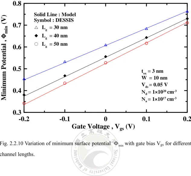
(11) Fig.2.1.12 The dependence of threshold voltage roll-off ΔVth,s on channel length L for various silicon film thicknesses ...............................................................................................27 Fig.2.1.13 The dependence of threshold voltage roll-off ΔVth,s on channel length L for various drain biases..................................................................................................................27 Fig.2.1.14 Analytical solution of the subthreshold slope for single-gate MOSFETs compared with 2D numerical simulation results with the silicon film thickness as a varied parameter..29 Fig.2.1.15 Analytical solution of the subthreshold slope for single-gate MOSFETs compared with 2D numerical simulation results with the gate oxide thickness as a varied parameter....30 Fig.2.1.16 Analytical solution of the subthreshold slope for single-gate MOSFETs compared with 2D numerical simulation results with the drain bias as a varied parameter ....................30 Fig.2.2.1 Schematic of Tri-Gate (TG) MOSFETs with cut plane along x-direction ...............31 Fig.2.2.2 The contour plot of the electrostatic scaling length versus insulator thickness and silicon thickness .......................................................................................................................36 Fig.2.2.3 The decay of Fourier series Dn, Pn, and Qn coefficients versus the term number ....38 Fig.2.2.4 The 3-D potential distribution from the device simulator of DESSIS for double-gate device of Vgs=0V..................................................................................................40 Fig.2.2.5 The 3-D potential distribution from the model results for double-gate device of Vgs=0V .....................................................................................................................................40 Fig.2.2.6 The variation of the surface potential of Ф(x=0,z) and Ф(x=W, =z) with the normalized channel length position of z/Lg for the different gate biases of Vgs=0V and Vgs=0.2V ..................................................................................................................................41 Fig.2.2.7 The variation of the channel potential Ф(x,z) with the normalized channel height position of x/W for the different channel locations of z=15nm, z=20nm, and z=25nm..........41 Fig.2.2.8 The analytical potential contours with channel length of Lg=60nm (defined as solid line) as well as those simulated by the two-dimensional device simulator (defined as symbol) ....................................................................................................................................42 Fig.2.2.9 The analytical potential contours with channel length of Lg=80nm (defined as solid line) as well as those simulated by the two-dimensional device simulator (defined as symbol) ....................................................................................................................................43 Fig.2.2.10 Variation of minimum surface potential Φ min with gate bias Vgs for different channel lengths.........................................................................................................................45 Fig.2.2.11 The dependence of threshold voltage roll-off ΔVth,s on channel length L for various gate oxide thicknesses .................................................................................................49 ix.
(12) Fig.2.2.12 The dependence of threshold voltage roll-off ΔVth,s on channel length L for various silicon film widths.......................................................................................................50 Fig.2.2.13 The dependence of threshold voltage roll-off ΔVth,s on channel length L for various drain biases..................................................................................................................50 Fig.2.2.14 Analytical solution of the subthreshold slope for double-gate MOSFETs compared with 2D numerical simulation results with the silicon film width as a varied parameter..................................................................................................................................52 Fig.2.2.15 Analytical solution of the subthreshold slope for double MOSFETs compared with 2D numerical simulation results with the gate oxide thickness as a varied paramete .....53 Fig.2.2.16 Analytical solution of the subthreshold slope for double-gate MOSFETs compared with 2D numerical simulation results with the drain bias as a varied parameter....53 Fig.2.3.1 Three-dimensional structure illustration of a Tri-Gate (TG) MOSFET ...................54 Fig.2.3.2 Schematic of Tri-Gate (TG) MOSFETs: (a) Cross section through the channel of a TG MOSFET; The device can be equivalently composed of two-dimensional asymmetrical double-gate (ASDG) MOSFET with width of tsi as shown in (b) and symmetrical double-gate (SDG) MOSFET with width of W as shown in (c)..............................................55 Fig.2.3.3 The variation of the bottom potential of Ф(x=W/2,y=tsi,z) with the normalized channel length position of z/Lg for the different gate biases of Vgs=0V, Vgs=0.1V and eff Vgs=0.2V. and the effective substrate bias of Vsub is also included for comparison................57. Fig.2.3.4 The 3-D potential distribution with cut plane along y-z direction from the device simulator of DESSIS for Tri-Gate (TG) device of Vgs=0V .....................................................58 Fig.2.3.5 The 3-D potential distribution with cut plane along y-z direction from the model results for Tri-Gate (TG) device of Vgs=0V.............................................................................58 Fig.2.3.6 The 3-D potential distribution with cut plane along x-z direction from the device simulator of DESSIS for Tri-Gate (TG) device of Vgs=0V .....................................................59 Fig.2.3.7 The 3-D potential distribution with cut plane along x-z direction from the model results for Tri-Gate (TG) device of Vgs=0V.............................................................................59 Fig.2.3.8 The analytical potential contours with channel length of Lg=40nm (defined as solid line) as well as those simulated by the two-dimensional device simulator (defined as symbol) ....................................................................................................................................60 Fig.2.3.9 The analytical potential contours with channel length of Lg=60nm (defined as solid line) as well as those simulated by the two-dimensional device simulator (defined as symbol) ....................................................................................................................................61 x.
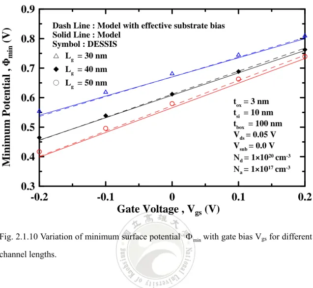
(13) Fig.2.3.10 Variation of minimum surface potential Фmin,TG with gate bias Vgs for different channel lengths.........................................................................................................................63 Fig.2.3.11 The dependence of threshold voltage roll-off ΔVth,TG on channel length L for various gate oxide thicknesses .................................................................................................65 Fig.2.3.12 The dependence of threshold voltage roll-off ΔVth,TG on channel length L for various silicon widths ..............................................................................................................66 Fig.2.3.13 The dependence of threshold voltage roll-off ΔVth,TG on channel length L for various silicon film thicknesses ...............................................................................................67 Fig.2.3.14 The dependence of threshold voltage roll-off ΔVth,TG on channel length L for various drain biases..................................................................................................................67 Fig.2.3.15 Analytical solution of subthreshold slope for the Tri-Gate (TG) device compared with 3D simulator results with the silicon film thicknesses as a varied parameter .................69 Fig.2.3.16 Analytical solution of subthreshold slope for the Tri-Gate (TG) device compared with 3D simulator results with the gate oxide thickness as a varied parameter ......................70 Fig.2.3.17 Analytical solution of subthreshold slope for the Tri-Gate (TG) device compared with 3D simulator results with the silicon widths as a varied parameter.................................70 Fig.3.1.1 Schematic cross-section view of an asymmetrical Tri-Material Tri-Gate (TMTG) SOI MOSFETs with cut plane along y-direction.....................................................................73 Fig.3.1.2 The 3-D potential distribution from the device simulator of DESSIS for tri-material single-gate device of Vgs=0V and L1:L2:L3=1:1:1 ................................................82 Fig.3.1.3 The 3-D potential distribution from the model results for tri-material single-gate device of Vgs=0V and L1:L2:L3=1:1:1......................................................................................82 Fig.3.1.4 The dependence of surface potential on the normalized channel length with different ratios of gate material regions, and the single-material gate (SMG) MOSFETs are also included for comparison ...................................................................................................83 Fig.3.1.5 The surface potential versus the normalized channel position with the different gate oxide thicknesses..............................................................................................................83 Fig.3.1.6 Variation of minimum surface potential Φ1min with gate bias Vgs for different channel lengths.........................................................................................................................85 Fig.3.1.7 Variation of minimum surface potential Φ1min with gate bias Vgs for different ratios of L1:L2:L3 ......................................................................................................................85. xi.
(14) Fig.3.1.8 The variation of the electric field with the normalized channel position for ratio of L1:L2:L3=1:1:1, and the single-material gate (SMG) MOSFETs are also included for comparison...............................................................................................................................87 Fig.3.1.9 The threshold voltage roll-off ΔVth,s versus the channel length L with the different ratios of L1:L2:L3 ......................................................................................................................93 Fig.3.1.10 The threshold voltage roll-off ΔVth,s versus the channel length L with the different gate oxide thicknesses ...............................................................................................93 Fig.3.1.11 The threshold voltage roll-off ΔVth,s versus the channel length L with the different silicon film thicknesses .............................................................................................94 Fig.3.1.12 The threshold voltage roll-off ΔVth,s versus the channel length L with the different drain biases................................................................................................................94 Fig.3.1.13 Analytical solution of the subthreshold slope for tri-material single-gate MOSFETs compared with 2D numerical simulation results for different ratios of L1:L2:L3 ..97 Fig.3.1.14 Analytical solution of the subthreshold slope for tri-material single-gate MOSFETs compared with 2D numerical simulation results with the gate oxide thickness as a varied parameter....................................................................................................................97 Fig.3.1.15 Analytical solution of the subthreshold slope for tri-material single-gate MOSFETs compared with 2D numerical simulation results with the silicon film thickness as a varied parameter....................................................................................................................98 Fig.3.1.16 Analytical solution of the subthreshold slope for tri-material single-gate MOSFETs compared with 2D numerical simulation results with the drain bias as a varied parameter..................................................................................................................................98 Fig.3.1.17 Analytical solution of the subthreshold current for tri-material single-gate MOSFETs compared with 2D numerical simulation results for different ratios of L1:L2:L3 ...... ................................................................................................................................................101 Fig.3.1.18 Analytical solution of the subthreshold current for tri-material single-gate MOSFETs compared with 2D numerical simulation results with the gate oxide thickness as a varied parameter..................................................................................................................101 Fig.3.1.19 Analytical solution of the subthreshold current for tri-material single-gate MOSFETs compared with 2D numerical simulation results with the silicon film thickness as a varied parameter..................................................................................................................102. xii.
(15) Fig.3.1.20 Analytical solution of the subthreshold current for tri-material single-gate MOSFETs compared with 2D numerical simulation results with the channel length as a varied parameter.....................................................................................................................102 Fig.3.2.1 Schematic cross-section view of an asymmetrical Tri-Material Tri-Gate (TMTG) MOSFET with cut plane along x-direction............................................................................103 Fig.3.2.2 The 3-D potential distribution from the device simulator of DESSIS for tri-material double-gate device of Vgs=0V and L1:L2:L3=1:1:1.............................................113 Fig.3.2.3 The 3-D potential distribution from the model results for tri-material double-gate device of Vgs=0V and L1:L2:L3=1:1:1....................................................................................113 Fig.3.2.4 The dependence of surface potential on the normalized channel length with different ratios of gate material regions, and the single-material double-gate (SMDG) MOSFETs are also included for comparison .........................................................................114 Fig.3.2.5 The surface potential versus the normalized channel position with the different gate oxide thicknesses............................................................................................................114 Fig.3.2.6 Variation of minimum surface potential Φ1min with gate bias Vgs for different channel lengths.......................................................................................................................116 Fig.3.2.7 Variation of minimum surface potential Φ1min with gate bias Vgs for different ratios of L1:L2:L3 ....................................................................................................................116 Fig.3.2.8 The variation of the electric field with the normalized channel position for ratio of L1:L2:L3=1:1:1, and the single-material double-gate (SMDG) MOSFETs are also included for comparison .......................................................................................................................118 Fig.3.2.9 The threshold voltage roll-off ΔVth,s versus the channel length L with the different ratios of L1:L2:L3 ....................................................................................................................124 Fig.3.2.10 The threshold voltage roll-off ΔVth,s versus the channel length L with the different gate oxide thicknesses .............................................................................................124 Fig.3.2.11 The threshold voltage roll-off ΔVth,s versus the channel length L with the different silicon widths ..........................................................................................................125 Fig.3.2.12 The threshold voltage roll-off ΔVth,s versus the channel length L with the different drain biases..............................................................................................................125 Fig.3.2.13 Analytical solution of the subthreshold slope for tri-material double-gate MOSFETs compared with 2D numerical simulation results for different ratios of L1:L2:L3 ...... ................................................................................................................................................128. xiii.
(16) Fig.3.2.14 Analytical solution of the subthreshold slope for tri-material double-gate MOSFETs compared with 2D numerical simulation results with the gate oxide thickness as a varied parameter..................................................................................................................128 Fig.3.2.15 Analytical solution of the subthreshold slope for tri-material double-gate MOSFETs compared with 2D numerical simulation results with the silicon width as a varied parameter.....................................................................................................................129 Fig.3.2.16 Analytical solution of the subthreshold slope for tri-material double-gate MOSFETs compared with 2D numerical simulation results with the drain bias as a varied parameter................................................................................................................................129 Fig.3.2.17 Analytical solution of the subthreshold current for tri-material double-gate MOSFETs compared with 2D numerical simulation results for different ratios of L1:L2:L3 ...... ................................................................................................................................................133 Fig.3.2.18 Analytical solution of the subthreshold current for tri-material double-gate MOSFETs compared with 2D numerical simulation results with the gate oxide thickness as a varied parameter..................................................................................................................133 Fig.3.2.19 Analytical solution of the subthreshold current for tri-material double-gate MOSFETs compared with 2D numerical simulation results with the channel width as a varied parameter.....................................................................................................................134 Fig.3.2.20 Analytical solution of the subthreshold current for tri-material double-gate MOSFETs compared with 2D numerical simulation results with the channel length as a varied parameter.....................................................................................................................134 Fig.3.3.1 Three-dimensional structure of Tri-Material Tri-Gate (TMTG) MOSFET............135 Fig.3.3.2 Schematic of tri-material tri-gate MOSFETs: (a) three-dimensional device structure, (b) with cut plane along B-B’ (c) with cut plane along A-A’. The device can be equivalently composed of two-dimensional asymmetrical tri-material double-gate (ASTMDG) MOSFET with width of tsi as shown in (b) and symmetrical tri-material double-gate (STMDG) MOSFET with width of W as shown in (c)......................................136 Fig.3.3.3 The 3-D potential distribution with cut plane along y-z direction from the device simulator DESSIS of ISE-TCAD for tri-material tri-gate (TMTG) device of Vgs=0V and L1:L2:L3=1:1:1 .......................................................................................................................140 Fig.3.3.4 The 3-D potential distribution with cut plane along y-z direction from the model results for tri-material tri-gate (TMTG) device of Vgs=0V and L1:L2:L3=1:1:1 ....................140. xiv.
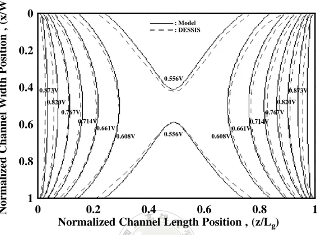
(17) Fig.3.3.5 The 3-D potential distribution with cut plane along x-z direction from the device simulator DESSIS of ISE-TCAD for tri-material tri-gate (TMTG) device of Vgs=0V and L1:L2:L3=1:1:1 .......................................................................................................................141 Fig.3.3.6 The 3-D potential distribution with cut plane along x-z direction from the model results for tri-material tri-gate (TMTG) device of Vgs=0V and L1:L2:L3=1:1:1 ....................141 Fig.3.3.7 The dependence of bottom potential on the normalized channel length with different ratios of gate material regions for tri-material tri-gate MOSFET and the single-material tri-gate (SMTG) MOSFETs are also included for comparison.....................142 Fig.3.3.8 The bottom potential versus the normalized channel position (z/Lg) with the different gate oxide thicknesses for the tri-material tri-gate (TMTG) MOSFET ..................142 Fig.3.3.9 The bottom potential distribution versus the normalized channel position (z/Lg) for different drain biases for the tri-material tri-gate (TMTG) MOSFET. The SMTG MOSFETs are also included for comparison ...........................................................................................143 Fig.3.3.10 Variation of minimum bottom potential Ф1min,TMTG with gate bias Vgs for different channel lengths.......................................................................................................................145 Fig.3.3.11 Variation of minimum bottom potential Ф1min,TMTG with gate bias Vgs for different ratios of L1:L2:L3 ....................................................................................................................145 Fig.3.3.12 The variation of the electric field with the normalized channel position for ratio of L1:L2:L3=1:1:1, and the single-material tri-gate (SMTG) MOSFETs are also included for comparison.............................................................................................................................147 Fig.3.3.13 The two-dimensional analytical potential contours for TMTG MOSFETs that are compared to those simulated by the device simulator DESSIS of ISE-TCAD. The simulated device parameters are tox =3 nm, tsi =10 nm, W =10 nm, tbox =100 nm, L1=40 nm, L2=40 nm, L3=40 nm, Na = 1ä1017 cm-3, Nd = 1ä1020 cm-3, ΦM1=4.77 eV, ΦM2=4.4 eV and ΦM3=4.17 eV...........................................................................................................................................148 Fig.3.3.14 The dependence of threshold voltage roll-off on channel length for different gate material ratios of L1:L2:L3 ......................................................................................................151 Fig.3.3.15 The dependence of threshold voltage roll-off on channel length for different gate oxide thicknesses ...................................................................................................................151 Fig.3.3.16 The dependence of threshold voltage roll-off on channel length for different silicon film thicknesses ..........................................................................................................152 Fig.3.3.17 Analytical solution of the subthreshold slope for tri-material tri-gate (TMTG) MOSFETs compared with 3D numerical simulation results for different ratios of L1:L2:L3 ...... ................................................................................................................................................155 xv.
(18) Fig.3.3.18 Analytical solution of the subthreshold slope for tri-material tri-gate (TMTG) MOSFETs compared with 3D numerical simulation results with the gate oxide thickness as a varied parameter..................................................................................................................155 Fig.3.3.19 Analytical solution of the subthreshold slope for tri-material tri-gate (TMTG) MOSFETs compared with 3D numerical simulation results with the silicon film thickness as a varied parameter..................................................................................................................156 Fig.3.3.20 Analytical solution of the subthreshold slope for tri-material tri-gate (TMTG) MOSFETs compared with 3D numerical simulation results with the drain bias as a varied parameter................................................................................................................................156 Fig.3.3.21 Analytical solution of the subthreshold current for tri-material tri-gate (TMTG) MOSFETs compared with 3D numerical simulation results for different ratios of L1:L2:L3 ...... ................................................................................................................................................158 Fig.3.3.22 Analytical solution of the subthreshold current for tri-material tri-gate (TMTG) MOSFETs compared with 3D numerical simulation results with the channel length as a varied parameter.....................................................................................................................159 Fig.3.3.23 Analytical solution of the subthreshold current for tri-material tri-gate (TMTG) MOSFETs compared with 3D numerical simulation results with the gate oxide thickness as a varied parameter..................................................................................................................159 Fig.4.1 Schematic of tri-gate MOSFETs: (a) three-dimensional device structure. With cut plane along AA’ and BB’, the device can be equivalently composed of two-dimensional symmetrical double-gate (SDG) MOSFET with width of W as shown in (b) and asymmetrical double-gate (ASDG) MOSFET with width of tsi as shown in (c). The two-dimensional device structures of Fig. 4.1 (b) and Fig. 4.1 (c) are used to derive the model, where regions 1, 3, and 2 denote the fresh and damaged zones, respectively ...........164 Fig.4.2 The dependence of channel potential on the normalized channel position for the different ratios of damaged zone to undamaged zone ...........................................................169 Fig.4.3 The variation of the two-dimensional potential distribution with the channel length and channel height for the simulation (The blue plot is for the damaged device with the positive trapped charges, the green plot is for the fresh device, and the red plot is for the damaged device with the negative trapped charges)..............................................................170 Fig.4.4 The variation of the two-dimensional potential distribution with the channel length and channel height for the model results (The blue plot is for the damaged device with the positive trapped charges, the green plot is for the fresh device, and the red plot is for the damaged device with the negative trapped charges)..............................................................170 xvi.
(19) Fig.4.5 Threshold voltage degradation versus normalized damaged zone for different thicknesses of silicon body ....................................................................................................174 Fig.4.6 Threshold voltage degradation versus normalized damaged zone for different thicknesses of gate oxide .......................................................................................................175 Fig.4.7 Threshold voltage degradation versus normalized damaged zone for different channel widths .......................................................................................................................175 Fig.4.8 Threshold voltage roll-off versus gate length for both fresh and damaged devices ..176 Fig.4.9 Threshold voltage degradation versus normalized damaged zone for DG, TG, and QG MOSFETs........................................................................................................................176 Fig.5.1 The three dimensional (3-D) structure for DMTG SOI MOSFETs which is made of two gate electrodes (M1 and M2) having different work functions. The symbols and axes used for modeling are also indicated .....................................................................................179 Fig.5.2 The decay of Fourier series Pn and Rn coefficients versus the term number .............188 Fig.5.3 The decay of Fourier series Tmn coefficients versus the term number ......................193 Fig.5.4 The 3-D potential distribution from the device simulator of DESSIS for DMTG SOI MOSFETs device L1 : L2 = 1 : 1, y = tsi and Vds = 1V ...........................................................195 Fig.5.5 The 3-D potential distribution from model results for DMTG SOI MOSFETs device L1 : L2 = 1 : 1, y = tsi and Vds = 1V.........................................................................................195 Fig.5.6 The 3-D potential distribution from the device simulator of DESSIS for DMTG SOI MOSFETs device L1 : L2 = 1 : 3, y = tsi and Vds = 1V ...........................................................196 Fig.5.7 The 3-D potential distribution from model results for DMTG SOI MOSFETs device L1 : L2 = 1 : 3, y = tsi and Vds = 1V.........................................................................................196 Fig.5.8 The 3-D potential distribution from the device simulator of DESSIS for DMTG SOI MOSFETs device L1 : L2 = 3 : 1, y = tsi and Vds = 1V ...........................................................197 Fig.5.9 The 3-D potential distribution from model results for DMTG SOI MOSFETs device L1 : L2 = 3 : 1, y = tsi and Vds = 1V.........................................................................................197 Fig.5.10 The 3-D potential distribution from the device simulator of DESSIS for DMTG SOI MOSFETs device L1 : L2 = 1 : 1, x = W/2 and Vds = 1V ................................................198 Fig.5.11 The 3-D potential distribution from model results for DMTG SOI MOSFETs device L1 : L2 = 1 : 1, x = W/2 and Vds = 1V..........................................................................198 Fig.5.12 The 3-D potential distribution from the device simulator of DESSIS for DMTG SOI MOSFETs device L1 : L2 = 1 : 3, x = W/2 and Vds = 1V ................................................199 Fig.5.13 The 3-D potential distribution from model results for DMTG SOI MOSFETs device L1 : L2 = 1 : 3, x = W/2 and Vds = 1V..........................................................................199 xvii.
(20) Fig.5.14 The 3-D potential distribution from the device simulator of DESSIS for DMTG SOI MOSFETs device L1 : L2 = 3 : 1, x = W/2 and Vds = 1V ................................................200 Fig.5.15 The 3-D potential distribution from model results for DMTG SOI MOSFETs device L1 : L2 = 3 : 1, x = W/2 and Vds = 1V..........................................................................200 Fig.5.16 The variation of the bottom potential with the normalized channel position for different ratios of gate lengths L1 and L2 of M1 and M2, respectively, keeping the sum (L1+L2 ) constant....................................................................................................................201 Fig.5.17 The variation of the bottom potential with the normalized channel position for different drain biases..............................................................................................................202 Fig.5.18 The variation of the bottom potential with the normalized channel position for different work functions.........................................................................................................202 Fig.5.19 Variation of minimum bottom potential with gate bias Vgs for different channel lengths ....................................................................................................................................204 Fig.5.20 Variation of minimum bottom potential with gate bias Vgs for different ratios of L1 to L2........................................................................................................................................204 Fig.5.21 The variation of the electric field with the normalized channel position for the different ratios of L1 and L2 ...................................................................................................206 Fig.5.22 The variation of the electric field with the normalized channel position for different drain biases.............................................................................................................................206 Fig.5.23 The 3-D electric field from the device simulator of DESSIS for DMTG SOI MOSFETs device L1 : L2 = 1 : 1, y = tsi and Vds = 1V ...........................................................207 Fig.5.24 The 3-D electric field from model result for DMTG SOI MOSFETs device. L1 :. L2 = 1 : 1, y = tsi and Vds = 1V................................................................................................207 Fig.5.25 Constant electrostatic potential contours based on the analytical solution (solid curves) for DMTG MOSFETs, compared with DESSIS simulation results (dash curve). Here, Vgs = 0.4V, Vds = 1V, L=80 nm, and L1 : L2 = 1 : 1 ......................................................208 Fig.5.26 The dependence of threshold voltage roll-off on the channel length with different ratios of L1 and L2 ..................................................................................................................214 Fig.5.27 The dependence of threshold voltage roll-off on the channel length with different work function of M2 ...............................................................................................................214 Fig.5.28 The variation of threshold voltage roll-off with channel length for different silicon film thicknesses......................................................................................................................215 Fig.5.29 The variation of threshold voltage roll-off with channel length for different silicon film widths .............................................................................................................................215 xviii.
(21) Fig.5.30 The variation of subthreshold swing versus the channel length for different ratios of L1 and L2 ............................................................................................................................219 Fig.5.31 The variation of subthreshold swing versus the channel length for different silicon film thicknesses......................................................................................................................220 Fig.5.32 The variation of subthreshold swing versus the channel length for different work functions.................................................................................................................................220 Fig.5.33 The subthreshold current versus the gate bias for the different ratios of L1 and L2 ...... ................................................................................................................................................223 Fig.5.34 The subthreshold current versus the gate bias for the different silicon widths .......223 Fig.5.35 The subthreshold current versus the gate bias for the different silicon thicknesses ...... ................................................................................................................................................224 Fig.5.36 The subthreshold current versus the gate bias for the different channel lengths.....224. xix.
(22) Chapter 1 INTRODUCTION 1.1 Motive of the Thesis For decades, progress in device scaling has followed an exponential curve, with the device density on a microprocessor doubling every three years. This has come to be known as Moore's law [1]. In an ever increasing need for higher current drive and better short-channel characteristics, silicon-on-insulator (SOI) MOS transistors are evolving from classical, planar, single-gate devices into three-dimensional devices with multiple gates (double-gate, tri-gate or quadruple-gate devices). These devices offer a higher current drive per unit silicon area than conventional MOSFETs. In addition, they offer optimal short-channel effects (reduced DIBL and subthreshold slope degradation). As CMOS devices have been scaled down, the channel length shrinks and the absolute value of threshold voltage becomes smaller due to the reduced controllability of the gate over depletion region by the increased charge-sharing from the source/drain. Fig. 1.1 shows the SOI MOSFETs ‘‘family tree’’ [2]. The first publication describing a double-gate SOI MOSFET dates back to 1984. The Tri-Gate or FinFET is the recent solutions for controlling SCEs and improving the subthreshold swing as well as packing densities. A group of leading companies publishes their projections for the next decade in the most recent International Technology Roadmap for Semiconductors (ITRS) [4], This roadmap projects a device gate-length of about 20nm for the year 2014. Scaling beyond ~20 nm, however, can be much more difficult. This is because we are close to the fundamental limits of semiconductor physics. The most important issue to be addressed is how much further can aggressive device scaling be continued. Multi-gate field-effect transistors (MuGFETs) such as Tri-Gate, FinFETs, have a strong potential for sub 32 nm technologies, which is in agreement with the ITRS roadmap.. 1.
(23) Fig. 1.1 SOI MOSFET family tree [2]. A numerous of literatures have modeled the hot-carrier-induced threshold voltage of planar and double-gate MOSFETs in the past decade. So far, very little work has been done on the analytical modeling of Tri-Gate (TG) MOSFETs including the localized interface trapped charges, although there have been some works studying the TG device performance through numerical simulation [5], or studying the device physics from experimental data [6]. To overcome limitations and realize high-performance MOS transistors, by considering effects of equivalent oxide charges on the flat-band voltage, effective conducting path, and poisson equation, a concise analytical subthreshold behavior model for TG MOSFETs with the interface trapped charges including threshold voltage, subthreshold slope, and subthreshold current are needed.. 2.
(24) Besides these new structures of TG or FinFET, we renew the top gate structure. The top and two side gate of the TG MOSFETs consists of two/three laterally contacting materials with different work-functions. This dual/tri Material gate structure takes advantage of material work-function difference leads that the threshold voltage near the source is larger than that near the drain, resulting in a more rapid acceleration of charge carriers in the channel and a screening effect to overcome short-channel effects [3]. Hence, Dual-Material Gate/Tri-Material Gate MOSFETs promise simultaneous suppression of SCEs, enhancement of average carrier velocity in the channel, and alleviation of reduced threshold problems using gate material engineering.. 3.
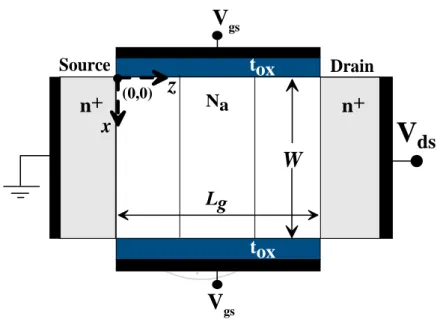
(25) 1.2 Tri-Gate Device Overview The Schematic of TG MOSFETs is shown in Fig. 1.2. The devices consist of a top and two side gates on an insulating layer. To avoid solving for 3-D Poisson equation that is too complicated to be derived, the 3-D TG device can be replaced with the 2-D equivalent asymmetric and symmetric double-gate structures by ignoring the coupling effects for assuming that channel length/channel width and channel length/channel thickness is larger than 2 which fall within the restrictions required to obtain realistic and operational TG devices [7].. B'. Vgs Gate Drain. Source (0,0). B. Drain. Vds. n+ Gate. Lg. W. n+. Vds. Lg. Source. Vgs. tsi A. Na. x n+. tox. n+. A'. z. Gate. (b). Vgs Gate. W W. Source. Drain (0,0). y. z. Na. tsi. n+. tbox. n+. Vds. Lg. Buried Oxide substrate. tbox. Vsub. Buried Oxide substrate. (a). Vsub. (c). Fig. 1.2 Schematic of Tri-Gate MOSFETs: (a) three-dimensional device structure, (b) with cut plane along A-A’ (c) with cut plane along B-B’. The device can be equivalently composed of two-dimensional symmetrical double-gate (SDG) MOSFET with width of W as shown in (b) and asymmetrical double-gate (ASDG) MOSFET with width of tsi as shown in (c).. 4.
(26) A transition from bulk to multiple-gate fully depleted (FD) silicon-on-insulator MOSFETs offers higher current drive per unit silicon area and better short-channel immunity. The TG device improves on the planar devices which reduce drain-source current leakage, and the control of the gates on the channel in a TG MOSFET is stronger than that in a conventional MOSFET as the gate voltage is applied from several sides and not just from the top. In recent years, TG MOSFETs have received more attention than the planar MOSFETs in the high speed or high frequency applications. Comparing TG device to conventional bulk CMOS device at the same technology node, these non-planar devices are found to be competitive with similarly-sized bulk CMOS transistors. TG MOSFETs will be more promising for the future VLSI circuits. Therefore, exploitation and use of TG MOSFETs in memory circuits [7] require the physics-based transistor model [8-11]. The findings of the model are much useful to investigate hot-carrier-induced threshold voltage and offer the basic guidance for the design of memory device. Furthermore, three-dimensional (3-D) simulations of TG transistors with. gate lengths down to 30 nm show that the 30 nm TG device remains. fully depleted, with near-ideal subthreshold swing and excellent short channel characteristics, suggesting that the TG transistor could pose a viable alternative to bulk transistors in the near future [12].. 5.
(27) Chapter 2 TWO DIMENSIONAL SUBTHRESHOLD BEHAVIOR MODEL FOR SOI TRI-GATE MOSFETs 2.1 Two Dimensional Subthreshold Behavior Model for 2.1 SOI Single-Gate MOSFETs 2.1.1 Model Derivation The p-channel Tri-Gate (TG) y-direction cross-section is shown in Fig. 2.1.1, the symbols and axes used for modeling are also indicated in this figure. We assume that the impurity density is uniform in the channel region. The channel potential distribution is expressed by Φ ( y, z ) . According to the Poisson equation, the channel potential distribution can be written as eq.(2.1.1) [13].. ∂ 2Φ ( y, z ) ∂ 2Φ ( y, z ) qN a + = ∂y 2 ∂z 2 ε si. 0 ≤ y ≤ tsi , 0 ≤ z ≤ Lg. (2.1.1). Vgs Source (0,0). y. tox. z. Drain. Na. tsi n+. n+. Vds. Lg. tbox Buried Oxide substrate. Vsub Fig. 2.1.1 Schematic of Tri-Gate (TG) MOSFETs with cut plane along y-direction. 6.
(28) Where Na is the uniform doping concentration of the silicon film, tox is the gate oxide thickness, tbox is the buried oxide thickness, tsi is the silicon film thickness, Lg is the device channel length, and the y-axis is perpendicular and the z-axis is parallel to the channel length, respectively. By using the superposition method, the resultant solution Φ ( y, z ) can be composed with one-dimensional (1-D) potential solution V(y) and 2-D potential solution U(y,z) which satisfy the following 2-D Laplace equation and 1-D Poisson equation, respectively [14]. Φ( y, z ) = V ( y ) + U ( y, z ). (2.1.2). Substituting eq.(2.1.2) into eq.(2.1.1), we obtain ∂ 2U ( y, z ) ∂ 2V ( y ) ∂ 2U ( y, z ) qN a + + = ∂z 2 ∂y 2 ∂y 2 ε si. (2.1.3). 1-D Poisson equation ∂ 2V ( y ) qN a = ∂y 2 ε si. (2.1.4). ∂ 2U ( y, z ) ∂ 2U ( y, z ) + =0 ∂y 2 ∂z 2. (2.1.5). 2-D Laplace equation. 7.
(29) 2.1.2 2-D Boundary Conditions Value Problem The Poisson equation is solved by using the following boundary conditions: (A) At the top side, electric flux at the interface of silicon/gate oxide is continuous: ∂Φ ( y, z ) ∂y. y =0. =−. ε ox Vgs − V fb − Φ ( y, z ) × tox ε si. (0 ≤ z ≤ Lg ). (2.1.6). Where Vgs is the top gate bias, tox is the gate oxide thickness, εsi is permittivity of silicon (εsi =11.7×8.85×10-14 ), εox is permittivity of oxide (εox =3.9×8.85×10-14), and Vfb is the flat-band voltage of front bias given as the difference between gate material work function and silicon work function. V fb = φM , top − φsi. (2.1.7). φsi is the silicon work function, which is given by φsi = χsi +. Eg 2q. − φB. (2.1.8). Where Eg is the silicon bandgap at 300 K, χsi is the electron affinity of silicon, φB is the Fermi potential (= VT × ln( N a ni ) ), VT is the thermal voltage (=kT/q), and ni is the intrinsic carrier concentration. (B) At the bottom side, electric flux at the interface of silicon/buried oxide is continuous ∂Φ ( y, z ) ∂y. y = tsi. =. ε ox Vsub − V fb − Φ ( y, z ) × tbox ε si. (0 ≤ z ≤ Lg ). (2.1.9). Where Vsub is the substrate bias, tbox is the buried oxide thickness. (C) The potential at the source end is Φ ( y, z = 0) = Vbi. (0 ≤ y ≤ tsi ). (2.1.10). Where Vbi=VTln(NaNd/ni2) is the built-in potential at the interface between source/drain and channel and Vds is the drain bias [15]. (D) The potential at the drain end is Φ ( y, z = Lg ) = Vbi + Vds. (0 ≤ y ≤ tsi ) 8. (2.1.11).
(30) Note that (A) and (B) imply that a linear variation of potential goes inside the oxide and both of them is only valid for the very thin gate oxide. For the thick buried oxide, we need to use the effective back-gate bias to compensate the non-linearity of the potential distribution in the buried gate oxide [16]. The potential does not vary linearly inside the buried oxide at Vsub=0V. But when Vsub>0, the variation of potential with the bottom-gate bias will gradually become linear, it is because the bottom-gate bias effect alleviate the gate electric fields or even be predominant. To account for this nonlinearity, eff we use a modified boundary condition, where an effective substrate bias Vsub [16] is. introduced. ∂Φ ( y, z ) ∂y. y = tsi. eff ε ox Vsub − V fb − Φ( y, z ) = × ε si tbox. (0 ≤ z ≤ Lg ). (2.1.12). eff Vsub is defined by. eff Vsub = Vsub + Φ (tsi , Lg / 2) + tbox × (. 9. ∂Φ ( y, Lg / 2) ∂y. ). y = tsi. (2.1.13).
(31) 2.1.3 1-D Solution From boundary condition (A) and (B), we get. ∂V ( y ) ∂y ∂V ( y ) ∂y. =− y =0. = y = tsi. ε ox Vgs − V fb − V ( y ) × ε si tox. (2.1.14). ε ox Vsub − V fb − V ( y ) × ε si tbox. (2.1.15). Using eq.(2.1.14) and eq.(2.1.15), 1-D solution can be obtained as. V ( y) =. qN a 2 y + ay + b 2ε si. (2.1.16). where. a=. b=. 2ε oxε si (Vsub − Vgs ) − qN atsi ( tsiε ox + 2ε sitbox ) 2ε si ⎡⎣tsiε ox + ε si ( tox + tbox ) ⎤⎦. {(. 2ε ox t siε ox (Vgs − V fb ) + ε si ⎡⎣tbox (Vgs − V fb ) + tox (Vsub − V fb ) ⎤⎦ 2ε ox ( tsiε ox + ε si ( tox + tbox ) ). (2.1.17). )} − qN t t. a si ox. ( tsiε ox + 2tboxε si ) (2.1.18). 10.
(32) 2.1.4 Scaling Length By using separation method together with boundary condition, one obtains the following resultant solution of the two-dimensional Laplace equation. From eq.(2.1.5) and by letting. U ( y, z ) = Y ( y ) Z ( z ). (2.1.19). By substituting eq.(2.1.19) into eq.(2.1.5), we obtain Y '' ( y ) Z ( z ) + Y ( y ) Z '' ( z ) = 0. (2.1.20). eq.(2.1.20) divided by Y ( y ) Z ( z ) , one obtains Y '' ( y ) Z '' ( z ) + =0 Y ( y) Z ( z). (2.1.21). Z '' ( z ) Y '' ( y ) =− = k2 Z ( z) Y ( y). (2.1.22). By letting. We obtain Z ( z ) = a1e − kz + a2e kz. (2.1.23). Y( y ) = a3cos (ky ) + a4 sin(ky ). (2.1.24). Due to a3cos (ky ) + a4 sin(ky ) = a32 + a42 sin ( ky + θ ) , the eq.(2.1.19) can be rewritten as ∞. (. ). U ( y, z ) = ∑ a32 + a4 2 a1e − kn z + a2e kn z sin ( kn y + θ n ) n =1. (2.1.25). Let a32 + a42 × a1 = Pn ,. a32 + a42 × a2 = Qn. (2.1.26). and we obtain ∞. (. ). U ( y, z ) = ∑ Pn e − kn z + Qn e kn z sin ( kn y + θ n ) n =1. (2.1.27). Where kn (k=π/λ) is the eigenvalue equation for the scale length, θ n is triangular parameters. 11.
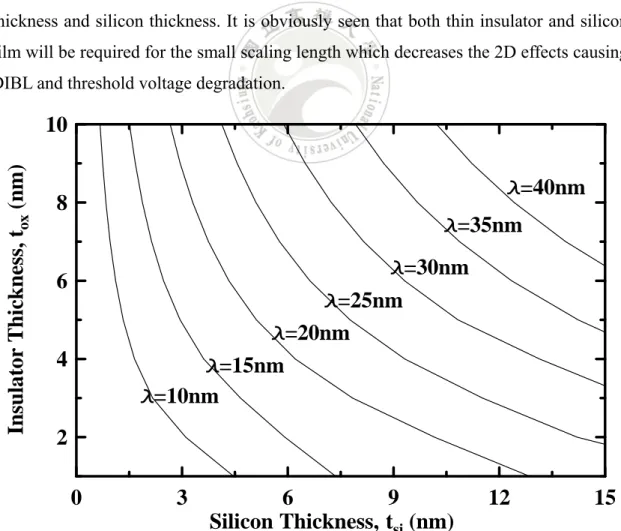
(33) From boundary condition (A) and (B), one obtain ∂U ( y, z ) ∂y ∂U ( y, z ) ∂y. =. ε ox U ( y, z ) × ε si tox. (2.1.28). =. ε ox −U ( y, z ) × ε si tbox. (2.1.29). y =0. y = tsi. From eq.(2.1.28) and (2.1.29), we obtain tan kntsi = tan θ n =. ε oxε si kn ( tox + tbox ) ε si 2 kn 2toxtbox − ε ox 2. (2.1.30). ε sitox kn ε ox. (2.1.31). Fig. 2.1.2 shows the contour plot of the electrostatic scaling length versus insulator thickness and silicon thickness. It is obviously seen that both thin insulator and silicon film will be required for the small scaling length which decreases the 2D effects causing DIBL and threshold voltage degradation.. Insulator Thickness, tox (nm). 10 λ=60nm 8. λ=50nm λ=40nm. 6 λ=30nm λ=20nm. 4. λ=10nm 2 0. 4 8 Silicon Thickness, tsi (nm). 12. Fig. 2.1.2 The contour plot of the electrostatic scaling length versus insulator thickness and silicon thickness. 12.
(34) 2.1.5 Coefficients Solution The Fourier series coefficients of Pn, Qn, Cn and Dn in the resultant solution of the two-dimensional Laplace equation can are expressed as k L. Pn =. Cn e n g − Dn 2sinh(kn Lg ). (2.1.32). −k L. −Cn e n g + Dn Qn = 2sinh(kn Lg ). (2.1.33). with. Cn = Dn =. −2qN a. γ − 4aη + 4 (Vbi − b ) ρ. (2.1.34). −2qN a. γ − 4aη + 4 (Vbi + Vds − b ) ρ. (2.1.35). ε si. ε si. Where γ, η and ρ in above equations are defined as. γ =. cos ( kn tsi + θ n ) ( 2 − kn 2 tsi 2 ) − 2 cos θ n + 2tsi kn sin ( kn tsi + θ n ) 2tsi kn 3 − kn 2 sin ( 2 ( kn tsi + θ n ) ) + kn 2 sin 2θ n. ⎡sin ( kntsi + θ n ) − sin θ n − kntsi cos ( kntsi + θ n ) ⎤⎦ η=⎣ 2tsi kn 2 − kn sin ( 2 ( kntsi + θ n ) ) + kn sin 2θ n. ρ=. cos θ n − cos ( kntsi + θ n ). 2tsi kn − sin ( 2 ( kntsi + θ n ) ) + sin 2θ n. 13. (2.1.36). (2.1.37). (2.1.38).
(35) Fig. 2.1.3 shows the decay of Fourier series Pn, Qn and Dn coefficients versus the term number. Since the Fourier series coefficients decay rapidly, the first term of Pn, Qn, and Dn will dominate the whole series and be used to derive the threshold voltage according to the minimum surface potential [17].. Coefficient(Pn,Qn,Dn). 0.8 : Dn : Pn : Qn. 0.6 0.4 0.2. tox = 3 nm tsi = 10 nm tbox = 100 nm Lg= 40 nm Vgs= 0 V Vds= 0.05 V Vsub= 0 V Na=1â1017 cm-2 Nd=1â1020 cm-2. 0 -0.2 0. 4. 8 Term Number , n. 12. 16. Fig. 2.1.3 The decay of Fourier series Dn, Pn, and Qn coefficients versus the term number.. 14.
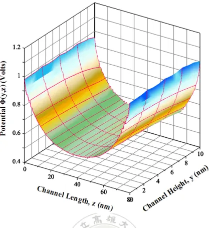
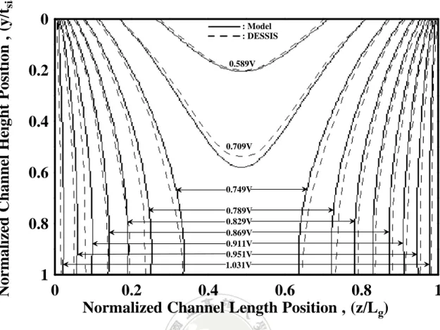
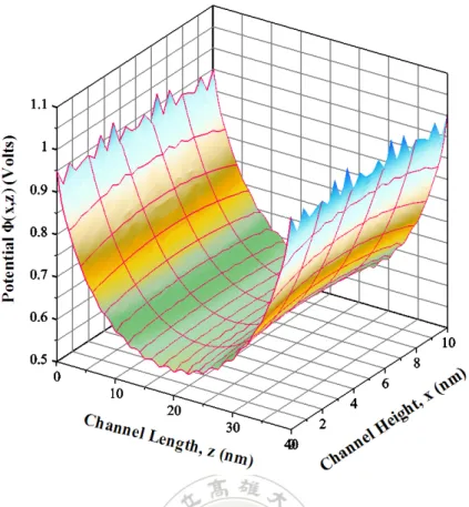
(36) 2.1.6 2-D Generalized Potential Model The full expression for the potential in silicon channel region is ∞ qN a 2 y + ay + b + ∑ Pn e − kn z + Qne kn z sin ( kn y + θ n ) 2ε si n =1. (. ). (2.1.39). To verify the analytical body potential model, Fig. 2.1.4 shows the 3-D potential distribution from the device simulator of DESSIS [18]. Fig. 2.1.5 shows the 3-D potential distribution from the model results. It is obviously seen that a close agreement for the 3-D potential distribution between the device simulator and analytical model are obtained. Fig. 2.1.6 shows the variation of the potential Ф(y=0,z) and Ф(y=tsi,z) with the normalized channel length position z/Lg for the different gate biases of Vgs=0V and eff is also included for comparison. A Vgs=0.2V and the effective substrate bias of Vsub. good agreement between the results calculated from our model with those simulated using the device simulator is obtained. It is observed that when the gate bias Vgs is increased from 0V to 0.2V, the minimum potential for both surface at y=0 and y=tsi are increased. Fig. 2.1.7 shows the variation of the channel potential Ф(y,z) with the normalized channel height position y/tsi for the different channel locations of z=15nm, eff is also included for z=20nm, and z=25nm and the effective substrate bias of Vsub. comparison. It can be seen that at the middle of the channel of z=25nm, the potential of Ф(y=0,z) and Ф(y=tsi,z) is smaller than that for the location of z=10nm and z=15nm. It implies that the device turn-on point will easily occur at the middle of the surface.. 15.
(37) Fig. 2.1.4 The 3-D potential distribution from the device simulator of DESSIS for single-gate device of Vgs=0V.. Fig. 2.1.5 The 3-D potential distribution from the model results for single-gate device of Vgs=0V. 16.
(38) Potential, F (y,z)(V). 1.2 tox=3 nm Dash Line : Model with effective substrate bias tsi=10 nm Solid Line : Model tbox=100 nm Symbol : DESSIS Vds=0.05 V + : Bottom potential Vsub = 0.0 V & : Surface potential Na=1â1017 cm-2 Nd=1â1020 cm-2. 1. Vgs=0.2 V. 0.8. Vgs=0.0 V. 0.6. 0. 0.2 0.4 0.6 0.8 Normalized Channel Length Position , (z/Lg). 1. Fig. 2.1.6 The variation of the surface potential of Ф(y=0,z) and Ф(y=tsi,z) with the normalized channel length position of z/Lg for the different gate biases of Vgs=0V and eff is also included for comparison. Vgs=0.2V and the effective substrate bias of Vsub. Potential, F (y,z)(V). 0.75 tox=3 nm tsi=10 nm tbox=100 nm Vgs=0.0 V Vsub = 0.0 V Vds=0.05 V Na=1â1017 cm-2 Nd=1â1020 cm-2. 0.7 0.65. Dash Line : Model with effective substrate bias Solid Line : Model Symbol : DESSIS & : z=15 nm ( : z=20 nm + : z=25 nm. z=15 nm. z=20 nm. 0.6 0.55 z=25 nm. 0.5 0. 0.2 0.4 0.6 0.8 Normalized Channel Height Position , (y/tsi). 1. Fig. 2.1.7 The variation of the channel potential Ф(y,z) with the normalized channel height position of y/tsi for the different channel locations of z=15nm, z=20nm, and eff is also included for comparison. z=25nm and the effective substrate bias of Vsub. 17.
(39) 2.1.7 Potential Contour Fig. 2.1.8 and Fig. 2.1.9 show the analytical potential contours and simulated data by the two-dimensional device simulator with variable channel length at Lg=60nm and Lg =80nm. A close agreement between them is observed, which further verifies the accuracy of our model. It is seen that the potential contours under the gate bend vertically into the channel, which implies that the electric fields from the gate will penetrate the channel and control the threshold behavior [19]. Among Fig. 2.1.8 and Fig. 2.1.9, it can be seen that with the increase in the channel length of Lg, the potential contour value from the gate in Lg=80nm is smaller than Lg=60nm due to more vertical. Normalized Channel Height Position , (y/tsi). electric lines into the channel.. 0. : Model : DESSIS 0.628V. 0.2 0.669V. 0.4 0.709V. 0.6. 0.749V 0.789V. 0.8. 0.829V 0.869V 0.911V 0.951V 1.031V. 1 0. 0.2 0.4 0.6 0.8 Normalized Channel Length Position , (z/Lg). 1. Fig. 2.1.8 The analytical potential contours with channel length of Lg=60nm (defined as solid line) as well as those simulated by the two-dimensional device simulator (defined as symbol).. 18.
(40) Normalized Channel Height Position , (y/tsi). 0. : Model : DESSIS 0.589V. 0.2 0.4. 0.709V. 0.6 0.749V 0.789V 0.829V 0.869V 0.911V 0.951V 1.031V. 0.8 1 0. 0.2 0.4 0.6 0.8 Normalized Channel Length Position , (z/Lg). 1. Fig. 2.1.9 The analytical potential contours with channel length of Lg=80nm (defined as solid line) as well as those simulated by the two-dimensional device simulator (defined as symbol).. 19.
數據
+7
相關文件
細目之砂紙,將絕緣體 及內部半導電層鉛筆狀
而在後續甲烷化反應試驗方面,以前段經厭氧醱酵產氫後之出流水為進流基 質。在厭氧光合產氫微生物方面,以光合作用產氫細菌中產氫能力最好的菌株 Rhodopseudomonas palustris
• 雙極性電晶體 (bipolar junction transistor , BJ T) 依結構區分,有 npn 型及 pnp 型兩種. Base
導體 絕緣體 電解質 非電解質.
探討燃燒所得的碳簇、活性碳及二氧化錳對 雙氧水分解的影響。將 3個100 mL量筒中各加 入 5 mL雙氧水和1 mL的清潔劑水溶液,分別 加入 0 .2 g碳黑、0.2
經過多次實驗後,團隊發現研發出的寡聚 物附著在一遇到高溫就會釋放出氧氣的正極材
• 雙極性電晶體 (bipolar junction transistor , BJ T) 依結構區分,有 npn 型及 pnp 型兩種. Base
酸性氣體(二氧化硫、二氧化氮)可以飄浮到離源頭很遠的地
![HPSH [ 氧化數平衡反應式係數 ]](data:image/gif;base64,R0lGODlhAQABAIAAAP///wAAACH5BAEAAAAALAAAAAABAAEAAAICRAEAOw==)