國 立 交 通 大 學
電子工程學系 電子研究所碩士班
碩 士 論 文
探討高閘極介電層N通道金氧半電晶體的
新穎閘極電流隨機電報量測法
The Observation of Gate Current Instability in High-k Gate
Dielectric MOSFET by a New Gate Current Random
Telegraph Noise Approach
研 究 生 :張家銘
指導教授 :莊紹勳 博士
探討高閘極介電層N通道金氧半電晶體的
新穎閘極電流隨機電報量測法
The Observation of Gate Current Instability in High-k
Gate Dielectric MOSFET by a New Gate Current
Random Telegraph Noise Approach
研 究 生 : 張家銘 Student : Chia-Ming Chang
指導教授 : 莊紹勳 博士 Advisor : Dr. Steve S. Chung
國立交通大學
電子工程學系 電子研究所碩士班
碩士論文
A Thesis
Submitted to Department of Electronics Engineering & Institute
of Electronics College of Electrical and Computer Engineering
National Chiao Tung University
In Partial Fulfillment of the Requirements
For the Degree of Master
In
Electronics Engineering
July 2008
Hsinchu, Taiwan, Republic of China.
探討高閘極介電層N通道金氧半電晶體的
新穎閘極電流隨機電報量測法
學生:張家銘 指導教授:莊紹勳博士
國立交通大學電子工程學系電子研究所碩士班
摘要
為了符合低功率的要求,閘極高介電材質的使用隨著閘級氧化層
的微縮越來越有取代二氧化矽的趨勢。除了可以得到一樣的等效氧化
層厚度之外,還可以明顯降低閘極漏電流超過三個數量級。但是高介
電材質閘極有許多的可靠度問題,主要是來自於高介電閘極層中有許
多缺陷抓取電荷,因此在實際電路操作時,會產生臨界電壓,汲極電
流等的不穩定。
本論文中,將使用一個新的方法,稱作「閘極電流隨機電報訊號」
方法來分析高介電材料閘極層中電荷抓取及放出的現象。透過給一固
定的閘極電壓觀察閘極電流,閘極直接穿隧電流會在多個層次間振
動,其原因來自於電荷在穿越閘極層時,會掉進閘極層裡面的缺陷並
被抓住,但又容易藉著熱從缺陷中散逸。當電荷被抓取時會降低閘極
穿隧電流,放出後電流又恢復,透過統計抓取及放出的時間,可以得
到缺陷的特性,另外藉由觀察電流振幅了解在電路上的影響。
我們運用此方法來觀察三種不同的缺陷,包括製程產生的缺陷、
元件經過不同電壓破壞之後產生的缺陷以及介電層在軟崩潰之後的
影響。由此方法觀察到的閘極電流不穩定性可判斷出閘極介電層的劣
化程度,不同程度的破壞會使電荷抓取及放出的機制受到影響。另外
藉由改變溫度量測,可以更有效的了解此現象並且得知元件的可靠
度。
The Observation of Gate Current Instability in High-k
Gate Dielectric MOSFET by a New Gate Current
Random Telegraph Noise Approach
Student:Chia-Ming Chang Advisors:Dr. Steve S. Chun
g
Department of Electrical Engineering & Institute of Electronics
National Chiao Tung University
ABSTRACT
In order to meet the requirement for low power circuit application, high-k gate dielectrics are being implemented in Si CMOS technologies with aggressive oxide thickness scaling. For the same EOT practical high-k gate dielectrics, one can provide significant reductions (>103) in the gate leakage. Reliability characteristics will be one of the primary goals of future development work, in which a large amount of traps in high-k bulk layer demonstrates the trapping and detrapping phenomena of carries. It causes the instability of threshold voltage, drain current, etc.
In this thesis, a newly method, Gate Current Random Telegraph Noise, will be utilized to analyze the phenomenon of carriers trapping/detrapping in high-k gate dielectrics. We observe gate current by biasing the gate at fixed voltage and gate direct tunneling current will show two or three levels. The cause is carriers trapping in the trap site during tunneling through gate dielectrics and detrapping by thermal emission. Gate current is suppressed when traps capture carriers and recovers as traps empty. By statistically extracting capture and emission time, we can understand the
trap properties. Besides, the influence will be understood by observing the variation of current fluctuation.
We then apply this method to study three types of traps, including process induced traps, stress induced traps at distinct stress voltages, and post soft-breakdown character. Through the observation of gate current instability the degradation of gate dielectrics can be recognized. The experiment result shows the capture/emission mechanism affected by degrees of degradation. On the other hand, the appearance of gate current random telegraph noise is effectively investigated by measuring at different temperatures and the reliability of devices can be well understood.
誌 謝
兩年的實驗室生活是精采豐富的,但同時也充滿艱辛與汗水。首先要感謝 的是我的指導教授:莊紹勳博士,老師給予的生活上與專業上的指導與建議,讓 我在學業上與研究上獲益良多並學習到對事物應有的嚴謹態度以及處理方法。除 此之外,對於課業外的生活技能、觀念的督促,讓我必須在此表達感謝之意。 感謝已畢業的亞峻、元亨、耀賢及大正學長當我在實驗遇到瓶頸和挫折時, 總是能耐心指導,並給予支持與鼓勵。也感謝在兩年研究生涯中,與我一起嚐遍 酸甜苦辣的同學,包括小郭、友良、文彥與易叡,我們一起經歷困苦的研究過程, 相信數年後再聚首,一定倍感溫馨。另外我要特別感謝汪老師研究群的小馬學 長,此研究論文唯有他無私的教導才能順利完成。對於汪老師研究群的同學,即 使我們身在不同的研究群,但我們的感情就像是一家人一樣,希望以後在業界相 遇時還能保有我們現在的真誠,也祝福大正、元亨、小馬、達達、阿豆肯與阿雄 學長能夠順利取得博士學位,此外也感謝振鵬、米華、健宏、安舜與專題生禎晏, 感謝有你們這群學弟妹平日對於實驗室的付出,使學長們能夠專心於研究上,在 此,輕遞一份真摯的祝福,希望明年亦能看見你們順順利利的畢業。 另外,還要特別感謝聯華電子在元件上與技術上的協助,還有我的女友育 瑄,在我學生生涯的最後階段陪我辛苦度過,使我能獲得碩士學位。 謹將這份榮耀獻給培養我多年的父母親Content
Chinese Abstract --- i
English Abstract --- iii
Acknowledgements --- v
Content --- vi
Figure Captions --- viii
Chapter 1 Introduction………..1
1.1 Background……….………1
1.2 The Motivation of this Work……….….….1
1.3 Organization of the Thesis……….….….2
Chapter 2 Random Telegraph Signal of Gate Current for Process Induced Traps in
High-k nMOSFETs………..…3
2.1 Experimental……….….…..3
2.1.1 Preface……….….…3
2.1.2 Device preparation and previous work………..…...4
2.1.3 IG RTN measurement system………...….4
2.1.4 Statistics……….…….…..4
2.2 Physical Model of 2-Levels in Gate Current Fluctuation……….………....5
2.2.1 Factor of Fluctuation………...………..5
2.2.2 Direct Tunneling Model………...……….5
2.3 The Observation for IG RTN of Process Induced Traps………..….………6
2.3.1 Gate Current Waveform……….….………..6
2.3.2 Capture and Emission Time……….…..………7
2.4 Result and discussion………...……….7
2.4.1 Trap Energy………...………8
2.4.2 Trap Depth………..…….10
2.4.3 Activation Energy………...….10
Chapter 3 Random Telegraph Signal of Gate Current for Stressed Devices in High-k
nMOSFETs………...30
3.1 PBTI in NMOSFETs with High-k Dielectrics……….………...30
3.1.1 Threshold Voltage Instability………..……….………...30
3.1.2 Trap Generation………..……….………....31
3.1.3 Fowler-Nordheim Stress Model of Electrons……….……….………....32
3.2 IG RTN in High and Low Positive VG Stress………..…32
3.2.1 I-V Characteristic………....33
3.2.2 Gate Current Waveform……….……….34
3.2.3 Capture and Emission Time……….……...34
3.3 Result and Discussion………....35
3.3.1 Trap Depth………..35
3.3.2 Trap Energy Variation………...36
3.3.3 Temperature Dependence……….……...37
3.3.4 Noise Amplitude………..37
Chapter 4 Random Telegraph Signal of Gate Current for Post Soft Breakdown
Devices in High-k nMOSFETs………56
4.1 Time Dependence Dielectric Breakdown……….……...56
4.1.1 Soft and Hard Breakdown……….…...56
4.1.2 Impact of Soft Breakdown on Device and Circuit Performance………..……57
4.2 IG RTN in Post Soft-Breakdown Devices……….……...58
4.2.1 Stress Condition………...58
4.2.2 I-V Characteristic……….59
4.3 Result and Discussion………..59
4.3.1 Gate Current Waveform………...59
4.3.2 Capture and Emission Time……….60
4.3.3 Model………61
Figure Captions
Chapter 2
Fig. 2.1 The operating procedure of following measurement applied to DUT.
Fig. 2.2 The measurement setup using Analyzer HP 4156C to sampling as RTN processing. Fig. 2.3 The terminals setup using Analyzer HP 4156C to sampling.
Fig. 2.4 Evolution of current for single electron capture and emission. (a) IG, (b) IS, (c) ID.
Fig. 2.5 Schematic plot of gate current instability due to trapped electrons. (a) Trap empty
state, (b) Trap filled state.
Fig. 2.6 Gate current waveform of high-k nMOSFETs with process induced trap (PIT1). Fig. 2.7 Gate current waveform of high-k nMOSFETs with process induced trap (PIT2).
Fig. 2.8 Variation of capture time τc (open symbol) and emission τe (filled symbol) as gate
voltage increasing (a) PIT1 (b) PIT2.
Fig. 2.9 Plot of electron occupation factor ft versus gate voltage (a) PIT1, (b) PIT2.
Fig. 2.10 Trap energy variation ∆ET to gate voltage plots (a) PIT1, (b) PIT2.
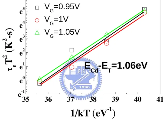
Fig. 2.11 τeT2 versus 1/kT plots for PIT1. Energy difference between conduction band of
dielectric and trap ECd-ET is around 1.06eV.
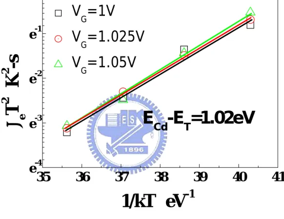
Fig. 2.12 τeT2 versus 1/kT plots for PIT2. Energy difference between conduction band of
dielectric and trap ECd-ET is around 1.02eV.
Fig. 2.13 (a) Energy band diagram at the trap position in the channel. (b)
Configuration-coordinate diagram for an acceptor trap. Open circle represents an empty trap and solid one is for a filled trap.
Fig. 2.14 Relationship of τc/τe to gate voltage. The extracted ZT from the slope is 5.7A and
3.8A for PIT1 and PIT2 respectively.
Fig. 2.15 Plot of τc/τe versus gate voltage at different temperature. The slope of plot at
different temperature is identical.
12 13 14 15 16 17 18 19 20 21 22 23 24 25 26
Fig. 2.16 Dependence of characteristic time to 1/kT on distinct gate voltages for PIT1 (a)
capture time, (b) emission time. Activation energy Ea is also expressed in the plot.
Fig. 2.17 Dependence of characteristic time to 1/kT on distinct gate voltages for PIT2 (a)
capture time, (b) emission time. The trend of Activation energy Ea is identical with
PIT1.
Fig. 2.18 Schematic plot of capture and emission mechanism. This is proven that electrons
could be captured by tunneling from substrate and emitted by Frankle-Poole emission.
Chapter 3
Fig. 3.1 Plot of trap density versus effective depth Zeff. This profile plot is derived by
Charge Pumping method.
Fig. 3.2 Typical procedure of following analysis in stressed devices. 3rd step “Stress “would
continue if 4th step “IG RTN” has no observation of 2 levels of gate current noise.
Fig. 3.3 Evolution of gate current during stress. (a) High-field stress, VG= 2.5V, (b)
Low-field stress, VG= 2.1V. Other terminals are grounded.
Fig. 3.4 ID-VG and IG-VG plots before and after high-field stress. Gate current is direct
tunneling current at low VG and F-N tunneling current appears at high VG. VD=
0.05V, VS= VB= 0V.
Fig. 3.5 ID-VG and IG-VG plots before and after low-field stress. VD= 0.05V, VS= VB= 0V.
Fig. 3.6 Schematic plot of F-N stress. (a) Low VG (b) High VG
Fig. 3.7 Gate current waveform of high-k nMOSFETs with high-field stress induced trap
(SIT1), T= 25℃.
Fig. 3.8 Gate current waveform of high-k nMOSFETs with low-field stress induced trap
(SIT2), T=25℃.
Fig. 3.9 Variation of capture time τc (open symbol) and emission τe (filled symbol) as gate
27 28 29 39 40 41 42 43 44 45 46 47
voltage increasing (a) SIT1 (b) SIT2.
Fig. 3.10 Electron occupation factor versus gate voltage plots (a) high field stress induced
trap (SIT1), (b) low field stress induced trap (SIT2).
Fig. 3.11 Schematic plots of band diagram in high-k dielectrics MOSFETs. (a) Electrons
tunneling from gate model and specific defined parameters, (b) relative trap energy position at low VG, (c) relative trap energy position at high VG.
Fig. 3.12 Capture time to emission time ratio versus gate voltage plots, (a) high field stress
induced trap (SIT1), (b) low field stress induced trap (SIT2).
Fig. 3.13 Trap energy variation respect to gate voltage plots (a) positive movement in high
field stress induced trap (SIT1) (b) negative movement in low field stress induced trap (SIT2).
Fig. 3.14 τeT
2
versus 1/T plots for SIT1. Energy difference between conduction band of dielectric and trap Ecd-ET is around 1.2eV.
Fig. 3.15 Dependence of characteristic time to 1/kT on distinct gate voltages for SIT1 (a)
capture time, (b) emission time. Activation energy Ea is also expressed in the plot.
Fig. 3.16 Diagram of electrons captured/emitted mechanism from channel or poly-gate.
Fig. 3.17 Magnitude of gate current plot, (a) SIT1, (b) SIT2.
Chapter 4
Fig. 4.1 Evolution of the gate voltage as the device suffered stress. Soft breakdown
occurrence and wear-out are represented in the plot.
Fig. 4.2 Gate and drain current versus gate voltage plots. Open square is the fresh one and
an inverted triangle is post soft breakdown one.
Fig. 4.3 Gate current waveform at different gate voltage during VG= 1.4V to 1.475V. Four
levels of gate current are obviously shown and two SBD paths exist.
Fig. 4.4 (a) Relation of SBD paths switch to gate current. (b) Low and high conductive state
48 49 50 51 52 53 54 55 63 64 65 66
involved with gate current versus gate voltage plot. ∆V between IG,low and IG,high is
0.16V.
Fig. 4.5 Dependence of capture time (filled symbol) and emission time (open symbol)
versus gate voltage plot.
Fig. 4.6 Temperature and gate voltage dependence of (a) capture time and (b) emission time.
The activation energy is extracted from the slope of log(τ) to 1/kT plot.
Fig. 4.7 τeT2 verus 1/kT plots at different gate voltage during VG= 1.45V to 1.55V. All the
plots have the same scale and ECd-ET from the slopes is 0.93eV approximately.
Fig. 4.8 Schematic plot of band diagram post SBD. Breakdown path occurs and near SBD
path trap will capture/emit electrons. Emission is through Frankle-Poole emission.
67
68
69
Chapter 1
Introduction
1.1 Background
The physical limitations of the conventional silicon dioxide as gate dielectric reached the point where films physical thickness of 15A, the gate leakage current exceeds the specifications (1A/cm2). To face this critical problem, high-k dielectrics have been introduced as hafnium based, zirconium, aluminum oxides. In fact, while keeping the EOT constant high-k dielectrics allow us to increase the physical thickness of the gate stack. Hence, the gate leakage can be reduced by 2 to 3 orders of magnitude. Although a large amount of effort that has been paid on the study of high-k gate dielectrics, many of critical problems still unknown. These problems include defects in the material which can lead to undesired transport through the dielectrics gate band structure induces polarity effects on the leakage and reliability. All of these stack properties lead to an anomalous behavior with respect to the conventional SiO2.
In aforementioned studies, several reliability issues for high-k gate dielectrics have been indentified: threshold voltage instability [1.1], stress induced film degradation [1.2], and dielectric breakdown [1.3]. Threshold voltage instability is due to the dynamics of carriers charging/discharging in pre-existing high-k bulk defects and negative bias temperature instability (NBTI) in pMOSFETs and positive bias temperature instability (PBTI) in nMOSFETs is the critical bottleneck of high-k gate dielectrics.
In recent years, approach in high-k abound with plenty of traps has been studied mostly by transient related methods [1.4][1.5]. Both they are used to look into the interface and near-interface property but the accuracy is challenged if only gate dielectric is heavily destroyed. Although charge pumping method is most reliable to profile the trap density in-depth of gate dielectric stack, some traps do not surely respond to trap/detrap carriers on fixed time (T=1/f) and these kind of traps would be absent using charge pumping method. Conventional I-V and C-V methods are less dependable for high-k dielectric, and hence pulse I-V measurement system is needed just only to precisely identify the characteristic high-k dielectrics MOSFETs. Nevertheless, it costs a lot for purchasing the instruments.
In this thesis, we propose a new method called “Gate Current Random Telegraph Noise (IG RTN)” which is developed to analyze quality and reliability of high-k dielectric MOSFETs. In this approach, the noise from pulse generator could be neglected and it also diminishes AC stress possibility that would destruct devices by charge pumping method. By IG RTN method, it is easy to understand how
single electron affects gate current through existing DC instrument.
1.3 Organization of the Thesis
Large amount of process induced traps exist in high-k dielectric bulk material as mentioned in many papers. We organize IG RTN method and utilize it to detect existing traps in high-k MOSFETs in
detail in Chapter 1. Proposed in Chapter 3 is method to profile stress induced traps behavior. For stress induced drain current positive bias temperature instability (PBTI) in high-k nMOSFETs, we apply Fowler-Nordhiem stress at constant voltage without elevating temperature and produce traps which cause apparent 2-levels of gate current noise. Chapter 4 discusses the characteristic and gate current fluctuation after soft breakdown. Finally in Chapter 5, the results of this thesis and suggestions for future works are summarized.
Chapter 2
Random Telegraph Signal of Gate Current for Process
Induced Traps in High-k MOSFETs
2.1 Experimental
2.1.1 Preface
Conventionally, BTI characterization is carried out by periodically interrupting stress to measure electrical parameters, introducing a switching delay between stress and measurement which may give rise to an imprecise or even incorrect result. Recently, a two frequency charge pumping measurement has been utilized to characterize high-k trap properties [2.1][2.2]. First, the charge-pumping current may be too small to be reliably measured in small-size devices at a lower frequency required to probe into the high-k layer. Second, due to the mixture of interface and high-k bulk traps, the two-frequency Charge-pumping method may not be viable when the high-k trap density is comparable to or even less than the interface trap density. Third, charge-pumping current may contain gate leakage as devices are stressed or heavily destroyed even wear out or soft breakdown happen.
In this chapter, a newly developed characterization technique named “Gate Current Random Telegraph Noise” for exploration of high-k and interfacial layer trap properties by measuring the gate current in small-area devices is presented. Single electron capture and emission could be observed. The physic of gate current instability is interpreted in Section 3.2. Based on the temperature and voltage dependence of single charge effect, an analytical model for tunneling mechanism is developed and traps parameters are extracted.
2.1.2 Device Preparation and Previous Work
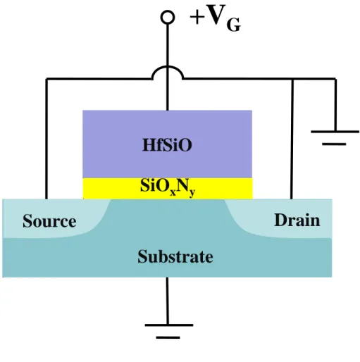
The devices used in this work are nMOSFETs with a poly-silicon electrode, and a bi-layered gate dielectric stack consisting of HfSiO and an interfacial SiOxNy layer. EOT of stacked dielectrics is 12A.
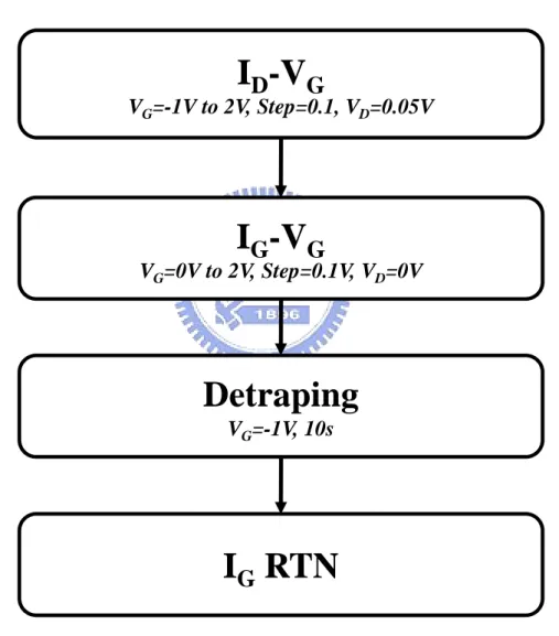
The gate width is 0.12µm~10µm, and the gate length range from 0.09µm~1µm. The complete procedure is shown in Fig. 2.1. The devices are first subjected to ID-VG and IG-VG measurement, and
then “detrap” at low negative gate voltage (VG= -1V, 10s). ID-VG is used to check out normal I-V
characteristic of devices and then we chose similar gate dielectric properties to compare that have most the same IG-VG. To avoid pre-existing electrons trapped in the dielectric affect gate current instability, a
“detrap” step is utilized before IG RTN.
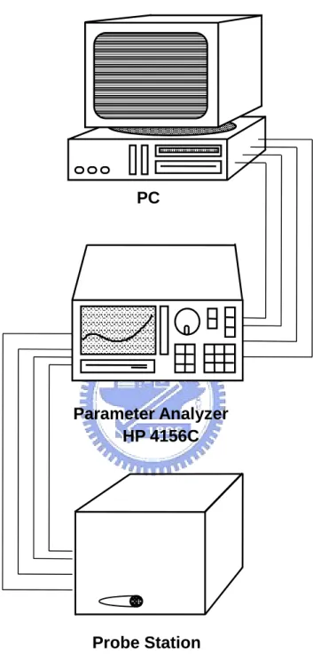
2.1.3 IG RTN measurement system
The measurement setup of IG RTN is shown in Fig. 2.2, Fig. 2.3. Gate current is about 10pA ~1nA,
three orders of magnitude or more smaller than drain current and hence probe station leakage path is more needed to be calibrated well. It is suggested to have parameter analyzer connecting to probe station directly without passing through switch equipment. On the other hand, large fluctuation may happen as probe needles don’t contact with the pad of wafer well, especially for body contact. The sampling rate is maximum 103 readings per second, that it means there is minimum 1ms of resolution. RTN phenomenon may be not observed as interval time set too larger due to capture or emission time less than the interval time. RTN happens only during local gate voltage so it’s better to detect varying tight gate voltage step as sampling. Otherwise, area of devices also affects IG RTN articulation;
generally it could be seen more clearly as area of devices going down but magnitude of gate current decreases relatively. So it is a trade-off to gain evidence of IG RTN.
The target of RTN measurement is to extract mean capture and emission time and then further profiles traps properties. Therefore, the switch of trap captures and emits electrons must be distinguished. We can determine using naked eye and it is also the most precise method to obtain mean capture and emission time. Nevertheless, it wastes time and not efficient for large amount of data. In our work, we write a program and used a current level that lies in the middle of the high and low current state to differentiate trap holding or releasing an electron automatically. Sequentially, every period of time was added and divided by numbers of events. Consequently, we extracted mean capture and emission time more accurately and can handle much larger amount of data also.
2.2 Cause of 2-Levels Gate Current Fluctuation
2.2.1 Factor of Fluctuation
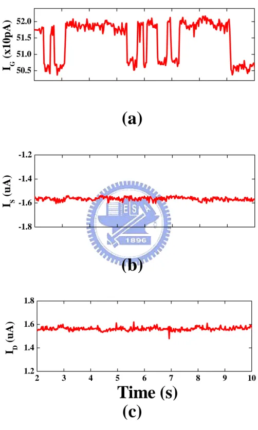
It is obvious that gate current is more responsible to electrons capture and emission in a trap site than drain/source current in Fig. 2.4. The amplitude, capture and emission time are the critical parameters of random telegraph noise phenomenon and they depend on the trap properties, such as trap depth into dielectrics, trap energy apart from conduction band (valance band if holes are captured and emitted) and magnitude of gate leakage current. Besides, retention of traps holding an electron and how much time an empty trap can capture an electron are also influenced by the electric field distributed among dielectrics and temperature that would involve in the probability of electrons hopping over activation energy mentioned in Chapter 2.
2.2.2 Direct Tunneling Model
Although high-k dielectrics have smaller effective oxide thickness than conventional insulator, SiO2,
direct tunneling current from the substrate to the gate through a trapezoid energy barrier as gate bias is around VG=1.2V. Fowler-Nordhiem tunneling current exists as gate bias larger than 1.8V. In our RTN
measurement, all used gate voltages for sampling are below 1.5V and large amount of gate current are direct tunneling current.
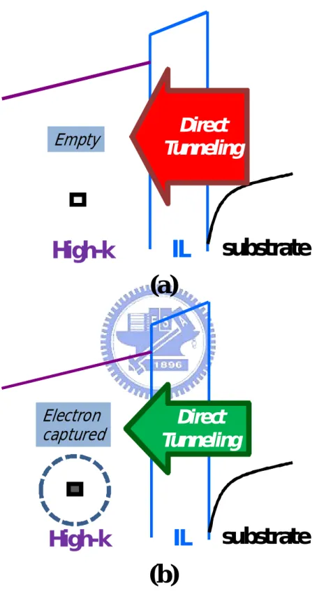
Gate current becomes smaller as an electron captured in the trap site in Fig. 2.5. The cause is electron trapped will screen the proximity of the trap and hence suppress the local direct tunneling current. It seems like a big stone laying in the flow of river so the flow rate is apparently rolling off. It is believed that the screen area is small compared with gate area and we know that trap induced direct tunneling current varied locally but not globally.
2.3 Process Induced Traps
2.3.1 Gate Current Waveform
In the following, we start to apply this method to analyze process induced traps behavior. It could not be seen absolutely in every device, and sometimes it is available to observe IG RTN phenomenon;
nevertheless analysis afterward is hard to process for some reasons, such as undistinguishable amplitude, multi-levels gate current states. Here below we show two valuable IG RTN measurement
results for process induced traps here and discuss the traps properties in later sections.
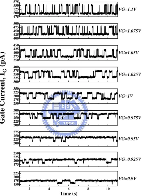
First one (PIT1) is measured at T=25℃ shown in Fig. 2.6. Traps start to capture electron as gate bias over 0.9V and then emission. As gate voltage increases, capture events happen more frequently. The events happen twice during 10 seconds at VG= 0.9V and over 40 times at VG= 1.1V. The other one
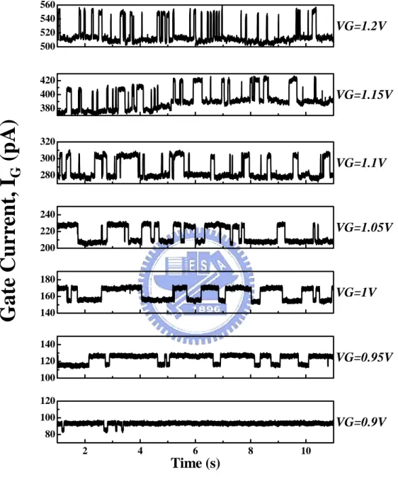
(PIT2) is shown in Fig. 2.7. Same trend happens with PIT1 as gate voltage varied but on different gate voltage, VG= 0.9V ~1.2V.
2.3.2 Capture and Emission Time
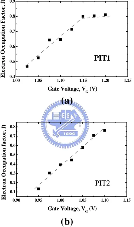
Fig. 2.8 shows the mean capture and emission time gathered statistics from Fig. 2.6 and Fig. 2.7. Capture time is affected by gate voltage and emission time keeps constant, i.e., the capture time relates to the electric field on dielectrics and electrons stride over barrier to trap sites by tunneling. On the other hand, emission time has no response to electric field and electrons escape does not go through tunneling possibly. Further study will be shown in Section 3.4. Electron occupation factor, ft defined
below is shown in Fig. 2.8 [2.3]. RTN is undetectable since the trap is always empty in weak inversion regime (i.e., VG< 0.9V). ft increases linearly in strong inversion regime since 40% at VG= 1V to 80% at
VG= 1.15V for PIT1, and saturates as gate voltage going up abidingly. ft of PIT2 also increases linearly
since 10% at VG=0.95V to 75% at VG=1.1V but not saturates yet. Electron occupation factor is
e c e t
f
τ
τ
τ
+
=
(2.1) Which is dominated by emission time that is too larger than capture time as we know from Eq. (2.1). Hence, the saturation happens when electron occupation factor is near the maximum “1”. This result is in accordance with the equilibrium case that ft (=1/(1+exp(ET-EF)/kT) increases as the trap energybecomes more negative with respect to the Fermi level.
2.4 Result and Discussion
Based on the Shockley–Read–Hall statistics [2.4], the carrier capture rate 1/τc can be written in
terms of the carrier density (per unit volume) n in the channel, the average velocity of the carriers v, and the average capture cross-section σ as Eq. (2.2), where
σ
τ
nv
c1
=
(2.2)⎟
⎠
⎞
⎜
⎝
⎛ ∆
−
=
kT
E
Bexp
0σ
σ
(2.3) the capture cross section is Eq. (2.3). Here σ0 is the cross-section prefactor, and ∆EB is the thermalactivation energy for capture. T and v are usually taken to be the equilibrium lattice temperature and average thermal velocity vth. This approximation is invalid at large lateral electric field, and electron
heating occurs and affects the electron capture time. Emission time is given as Eq. (2.4) [2.5], g is the
(
)
[
]
vn
g
T
k
E
E
F T B eσ
τ
=
exp
−
/
(2.4) degeneracy factor. The term (EF-ET) represents the trap energy with respect to the Fermi energy. kB arethe Boltzmann’s constant.
2.4.1 Trap Energy
From the principle of detailed balance, one can write the ratio of the mean emission time τe to mean
capture time τc as below. In nMOSFETs, as the gate bias is increased, the trap occupancy should
increase,
⎟
⎠
⎞
⎜
⎝
⎛
−
=
kT
E
E
g
T F e cexp
τ
τ
(2.5)⎥
⎥
⎦
⎤
⎢
⎢
⎣
⎡
⎟⎟
⎠
⎞
⎜⎜
⎝
⎛
−
⎟⎟
⎠
⎞
⎜⎜
⎝
⎛
=
−
0 0ln
ln
e c n e c T TnE
kT
E
τ
τ
τ
τ
(2.6)and, τc/τe consequently show a decrease. The change in the mark-space ratio of the switching signal
with respect to gate voltage indicates which transition corresponds to capture and which transition corresponds to emission of an electron. ET0 is reference trap energy at specific gate bias VG0, such as
VG0= 1.025V for PIT1, and ETn is trap energy at relative gate bias VGn as represented in Eq. (2.6). From
2.10. The variation is more obvious in PIT2 than in PIT2, and ∆ET/∆VG is about 20meV/0.1V for PIT1
and 50meV/0.1V for PIT2. It seems that these two traps distribute in different position of dielectrics and hence gate voltage produces distinct field change. Basically, trap sitting near poly-gate has larger variation as field changed in the same dielectric. From the measurement result, we may conclude that PIT1 is near the substrate and PIT2 is close to poly-gate but it s not the truth proven in the next section. The emission time constant is shown below [2.6], where NC is the effective conduction band densities
of state.
(
)
(
)
C T Cd e vN kT E Eσ
τ
= exp − / (2.7) ECd-ET is trap energy difference apart from conduction band of dielectric. The emission time constantsτe depends on the energy ET and the capture cross-section σ. The electron thermal velocity and
effective density of states in the conduction band are shown in Eq. (2.8), Eq.(2.9), allowing the emission time constant to be written as Eq. (2.10), where γ is a coefficient. A plot of ln(τe T2) versus
1/kT has s slope of (ECd-ET) and an intercept on the ln(τe T2) axis of ln(1/γσ).
n
m
kT
v
=
3
(2.8) 2 / 3 22
2
⎟
⎠
⎞
⎜
⎝
⎛
=
h
kT
m
N
n Cπ
(2.9)(
)
(
)
γσ
τ
eT2 = exp ECd-ET /kT (2.10)In our experiment shown in Fig. 2.10-2.11, ECd-ET is about 1.02eV and 1.06eV for PIT1 and PIT2
respectively. It can be seen that there is only a slight variation in ECd-ET as the gate voltage is
increasing. These values set the trap around the conduction band edge when compared to ϕ0 =3.1eV
[2.7] [2.8], the difference between the electron affinities of Si and IL, consistent with an acceptor trap acting as a repulsive center for electrons in the channel.
2.4.2 Trap Depth
By the principle of detailed balance, a relationship between the mean capture and emission times and trap parameters is found as Eq. 2.11 [2.9], where ECd, EC, EF, ϕ0 and ψs are defined in Fig. 2.13(a).
(
) (
)
(
)
⎥⎦⎤ ⎢⎣ ⎡ − − − − + + − − − = ⎟⎟ ⎠ ⎞ ⎜⎜ ⎝ ⎛ S FB G T S F C T Cd e c V V EOT q q E E E E kT ϕ ψ ψ τ τ 1 Z ln 0 (2.11) EOT kT q dV d T G e c Z ln − = ⎟⎟ ⎠ ⎞ ⎜⎜ ⎝ ⎛ τ τ (2.12)EOT is the effective oxide thickness and VFB is the flat-band voltage. We can estimate ZT, effective
depth from the substrate, from measurements of τc/τe by varying VG. ZT is 5.7A for PIT1and 3.8A for
PIT2 shown in Fig. 2.14. It means PIT1 sites into the gate dielectrics is deeper than PIT2 that is obviously contradictory to the assumption in Section 3.4.1. Hence, we could predict PIT1 and PIT2 lying in different type of dielectrics, that PIT1 is in high-k bulk layer and PIT2 is in the interfacial or transition layer. From the prediction, the measurement in Fig. 2.10 is reasonable because electric field variation in high-k bulk layer is small due to large permittivity. To extract reliable effective trap depth, the measurement is repeated in different temperature and result is shown in Fig. 2.15. They result in the same slope and ZT is extracted to same values as varying temperature.
2.4.3 Activation Energy
The capture and emission of an electron in the conduction band by a defect at the Si–IL interface can be explained utilizing a nonradiative multiphonon emission process. It is believed that the nonradiative multiphonon emission occurs due to the crossing of free electronic states with bound electronic states when sufficiently large lattice displacements exist. Before capturing an electron, the defect center will experience thermal vibrations around an equilibrium position close to the upper level
of the energy gap. After this capture, the defect would relocate at a new equilibrium position in the energy gap with shifted coordinates, creating violent lattice vibration at the defect. This instability subsides by damping down the vibration to the thermal vibration amplitude and emitting phonons. At lower temperatures, this relaxation takes longer time, effectively slowing down the switching events. This thermally activated behavior can be understood in terms of a configuration coordinate diagram of the trap (see Fig. 2.13(b)). An empty trap can be thermally excited to the crossover point B, where it can capture and electron from the silicon conduction band. The occupied trap then relaxes to its lowest stable level and dissipates the excess energy by multiphonon emission. The energy needed for emitting an electron is usually higher than that needed for capturing one [2.10]. The activation energies depend on the trap energy level relative to the silicon conduction band, and therefore, on band bending. Varying the gate voltage will affect the activation energies. This effect is larger in deep traps (larger ZT).
The plot of characteristic time to 1/kT is shown in Fig. 2.16-2.17. Firstly we see τc and τe increasing
intensely as temperature going down. For the capture time, electron thermal energy increases in the channel. Larger temperature enhances electrons hopping over activation energy barrier of capture
Ea,capture , same as emission, electrons held in trap have larger possibility to escape over activation
energy barrier of emission Ea,emission. Secondly both Ea,emission and Ea,emission are lower with gate bias.
Ea,capture is proven lower than Ea,emission here and decreases intensely as gate bias raising slightly, Ea,capture
varies around 0.38eV~0.61eV, as a result that gate bias would influence activation energy to capture of channel carriers. As illustrated in Fig. 2.18, time constant to tunnel from traps to poly-gate or back to substrate is much longer the time to Frankle-Poole emission.
Procedure
Detraping
V
G=-1V, 10s
I
G
RTN
I
D
-V
G
V
G=-1V to 2V, Step=0.1, V
D=0.05V
I
G
-V
G
V
G=0V to 2V, Step=0.1V, V
D=0V
Parameter Analyzer HP 4156C
PC
Probe Station
Fig. 2.2 The measurement setup using Analyzer HP 4156C to sampling as RTN
HfSiO
SiO
xN
ySource
Drain
Substrate
+V
G
50.5 51.0 51.5 52.0
I
G(
x10p
A)
(a)
-1.8 -1.6 -1.4 -1.2I
S(uA)
(b)
2 3 4 5 6 7 8 9 10 1.2 1.4 1.6 1.8I
D(uA)
Time (s)
(c)
Fig. 2.4 Evolution of current for single electron capture and emission. (a) IG, (b) IS, (c)
IL
High-k
substrate
Empty
Direct
Tunneling
(a)
IL
High-k
substrate
Electron
captured
Tunneling
Direct
(b)
Fig. 2.5 Schematic plot of gate current instability due to electrons trapped. (a) Trap
2 4 6 8 10 150 175 200 225 Time (s) VG=0.9V 175 200 225 250 VG=0.925V 200 225 250 275 VG=0.95V 200 225 250 275 300 VG=0.975V 250 275 300 325 350 VG=1V 300 325 350 375 400 VG=1.025V 350 375 400 425 450 VG=1.05V 400 425 450 475 500 VG=1.075V 475 500 525 550 575 VG=1.1V
Gate Curr
ent,
I
G(pA)
Fig. 2.6 Gate current waveform of high-k nMOSFET with process induced trap
2 4 6 8 10 80 100 120
Time (s)
VG=0.9V 100 120 140 VG=0.95V 140 160 180 VG=1V 200 220 240 VG=1.05V 280 300 320 VG=1.1V 380 400 420 VG=1.15V 500 520 540 560 VG=1.2VGate Curr
ent,
I
G
(pA)
Fig. 2.7 Gate current waveform of high-k nMOSFET with process induced trap
1.00 1.05 1.10 1.15 1.20 1.25
10-1
100
Gate Voltage, V
G(V)
Capture or Emission Time
(sec)
(a)
0.95 1.00 1.05 1.10
10-1 100
Capture or Emission Time (sec)
Gate Voltage, V
G(V)
(b)
Fig. 2.8 Variation of capture time τc (filled symbol) and emission τe (open symbol) as
1.00 1.05 1.10 1.15 1.20 1.25 0.4 0.5 0.6 0.7 0.8 0.9
Gate Voltage, V
G(V)
PIT1
Electron Occupation Factor,
ft
(a)
0.90 0.95 1.00 1.05 1.10 1.15 0.1 0.2 0.3 0.4 0.5 0.6 0.7 0.8Gate Voltage, V
G(V)
Electron Occupation factor,
ft
PIT2
(b)
1.03
1.08
1.13
1.18
-70
-60
-50
-40
-30
-20
-10
0
Gate Voltage, V
G(V)
Process induced
trap 1
Trap Energy Variation,
∆
E
T(meV
)
(a)
0.98
1.03
1.08
1.13
-170
-160
-150
-140
-130
-120
-110
-100
Trap Energy Variati
o
n,
∆
E
T(me
V
)
Gate Voltage, V
G(V)
Process induced
trap 2
(b)
35
36
37
38
39
40
41
e
-1e
0e
1e
2e
3e
4e
5V
G
=0.95V
V
G
=1V
V
G
=1.05V
1/kT
(
eV
-1
)
τ
e
T
2
(
K
2
-s
)
E
Cd
-E
T
=1.06eV
Fig. 2.11 τeT2 versus 1/kT plots for PIT1. Energy difference between conduction band
35
36
37
38
39
40
41
e
-4e
-3e
-2e
-1E
Cd
-E
T
=1.02eV
V
G=1V
V
G=1.025V
V
G=1.05V
1/kT
(
eV
-1
)
τ
e
T
2
(
K
2
-s
)
Fig. 2.12 τeT2 versus 1/kT plots for PIT2. Energy difference between conduction band
Ec
Ev
E
FE
Cd-E
TZ
Tϕ
0E
FgE
CgTrap
q
ψ
SChannel
IL
High-k
poly
(a)
E
a,captureE
a,emissionB
A
C
Normal Coordinate
(b)
Fig. 2.13 (a) Energy band diagram at the trap position in the channel.
(b) Configuration-coordinate diagram for an acceptor trap. Open circle represents an empty trap and solid one is for a filled trap.
1.00
1.05
1.10
1.15
1
2
Z
T
=3.8A
PIT2
PIT1
τ
c
/
τ
e
Gate Voltage, V
G(V)
Z
T
=5.7A
Fig. 2.14 Relationship of τc/τe to gate voltage. The extracted ZT from the slope is 5.7A
0.90
0.95
1.00
1.05
1.10
1
10
T=12.5
oC
T=25
oC
T=37.5
oC
T=50
oC
τ
c
/
τ
e
Gate Voltage, V
G(V)
Fig. 2.15 Plot of τc/τe versus gate voltage at different temperature. The slope of plot at
36
38
40
10
-210
-110
010
1Ea=0.38eV
Ea=0.49eV
V
G=1V
V
G=1.1V
V
G=1.2V
C
a
pture Time
(s
ec)
1/kT
(
eV
-1)
Ea=0.54eV
(a)
36
38
40
10
-210
-110
010
1Ea=0.45eV
Ea=0.48eV
V
G=1V
V
G=1.1V
V
G=1.2V
Em
is
sio
n
Ti
me
(se
c
)
1/kT
(
eV
-1)
Ea=0.55eV
(b)
Fig. 2.16 Dependence of characteristic time to 1/kT on distinct gate voltages for PIT1
(a) capture time, (b) emission time. Activation energy Ea is also expressed in
36
38
40
42
10
-210
-110
010
11/kT
(
eV
-1)
Ea=0.42eV
Ea=0.52eV
V
G=0.975V
V
G=1.025V
V
G=1.075V
C
a
pt
ure
Tim
e (s
ec
)
Ea=0.61eV
(a)
36
38
40
10
-210
-110
010
1Ea=0.50eV
Ea=0.52eV
Emiss
ion
Time
(s
ec
)
1/kT (eV
-1)
VG=0.975V VG=1.025V VG=1.075VEa=0.65eV
(b)
Fig. 2.17 Dependence of characteristic time to 1/kT on distinct gate voltages for PIT2
(a) capture time, (b) emission time. The trend of Activation energy Ea is
IL
High-k
Substrate
PIT2
PIT1
E
Cd-T1E
Cd-T2Direct
Tunneling
Frankle-Poole
Emission
E
CdFig. 2.18 Schematic plot of capture and emission mechanism. This is proven that
electrons could be captured by tunneling from substrate and emitted by Frankle-Poole emission.
Chapter 3
Random Telegraph Signal of Gate Current for Stressed Devices
in High-k nMOSFETs
3.1 PBTI in NMOSFETs with High-k Dielectrics
Bias Temperature Instability is a degradation phenomenon in MOSFETs. Even though the root causes of the degradation are not yet well understood, it is now commonly admitted that under a constant gate voltage and an elevated temperature, a build up of charges occurs either at the interface Si/SiO2 or in the oxide layer leading to the reduction of MOSFETs performances. Unlike SiO2, the
high-K dielectrics such as Hf-based dielectrics present serious instabilities for negative and positive bias (NBT), after NBT and PBT (Positive Bias Temperature) stresses. The trapped charges are sufficiently high to represent one of the high-k integration most critical show stopper that causes Vt
instabilities and drive current degradation. The instability is worrying, especially in the case of NMOS PBTI. It has been reported that the HfO2 MOSFETs is limited by nMOSFETs PBTI rather than
pMOSFETs PBTI [3.1]. In this section, we focus the discussion on NMOS only.
3.1.1 Threshold Voltage Instability
The NMOS PBTI reported in [3.2] shows an electron trapping (∆Vt >0). The main difference with
PMOS NBTI is that the whole Vt shift is recovered. That means that no interface traps are generated at
this gate bias stress. As for the NBTI, the PBTI characteristics display a logarithmic law and it can be well explained by the direct tunneling electron trapping. The trapping dynamic can be well explained by the model proposed by [3.3]. As explained below, the Vt shift during the stress can be well
explained by an electron tunneling from channel interface to the acceptor traps in the interfacial or high-k bulk layer, i.e.,
0 ln t t ox qN t V C α t ⎛ ⎞ ∆ = ⎜ ⎟ ⎝ ⎠ (3.1) The Vt could be characterized by pulsed Id-Vg method only and it is unreliable in D-C measurement
system due to transient carriers trapped happening in conventional Id-Vg and C-V methods. The
interfacial oxide thickness effect and the interface treatments on the Vt instability have also been
reported [3.4][3.5]. Like ∆Vt, saturation drain current Id.sat is heavily degraded owing to amounts of trap
generation near the channel. Unlike ∆Vt and Id.sat, sub-threshold swing and maximum transconductance
Gm,max do not change with stressing thereby indicating that interfacial trap generation is negligible
[3.6].
3.1.2 Trap Generation
Compared with SiO2, high-k based material dielectrics have severe reliability issue post stress
operation and affect regular I-V characteristics. In [3.7], the degradation is investigated to exhibits two stages, different degradation rate and stress temperature dependence. The drain current degradation in the first stage is attributed to the charging of pre-existing high-k dielectric traps while the degradation in the second stage is mainly due to additional high-k trap creation by transient measurement system. The two-stage degradation will affect the extrapolation of PBTI lifetime. The cause comes from lots of trap generated in the high-k bulk layer after stress and pre-existing traps would enhance another traps appearance that could be not happen in SiO2 dielectrics. Trap density at SiO2/Si interface, high-k/SiO2
interface, and high-k bulk layer are quantified respectively with a simple charge pumping method. We applied low frequency charge-pumping measurement [3.8] on our high-k dielectric devices as shown in Fig. 3.1. The following is the spatial distribution of interface trap:
( )
1( )
ln cp t m n t dQ N x qλ
A E d f = − ∆ (3.2)(
)
0 1 ln m m n n x tσ
vκ
= ⋅ (3.3) As a result, traps close to Si/SiOxNy interface have no significant increase. Toward the dielectric deeplyabout 3A that has the composition of SiOxNy only, not the transition region, the amount of traps is
much lower. Trap density is largely raising adjacent to HfSiO region and there is a maximum trap density about 5~ 8x10²¹ (cm-3) in transition area of SiOxNy /HfSiO interface. The IL thickness is about
4.2A apparently and trap density is stable over 4.2A. Post-stress trap density variation is also shown in the figure. There is considerable boost in HfSiO bulk region comparatively.
3.1.3 Fowler-Nordheim Stress Model of Electrons
Here, we discuss the dependence of ∆Vt from the injected electrons without considering
temperature dependence. It is obvious that increasing the voltage, a larger ∆Vt is observed for same
amount of injected electrons. The effect can be ascribed to three different causes; a generation of additional trap sites at higher voltages, a more effective electron trapping and/or a different spatial position of the trapped electrons within the dielectric stack [3.9]. In the next section, we will discuss F-N stress on high-k devices with distinct stress condition, while contain high and low field F-N stress and treat RTN phenomenon in great detail.
3.2 I
GRTN in High and Low Positive VG stress
The procedure of following experiment is shown in Fig. 3.2. There are same schedules in stressed devices measurement except for additional stress step. Some notable steps should be taken care. In ID-VG step, the purpose is to select the regular I-V characteristic devices with similar gate leakage and
magnitude of drain current. Aiming at the observation of RTN with stress induce traps, process induced traps noise is forbidden here and second step, IG RTN is used to ensure absence of PIT RTN.
Subsequently stress is adopted on selected devices. We applied F-N stress in inversion mode with injecting electrons to destruct gate dielectrics. Without elevating temperature here, we could prevent the effect of changing temperature and measure RTN at once. Two different stress conditions here; first one is high field (VG= 2.5V) and the other one is low field (VG= 2.1V). The evolutions of gate current
during stressing are shown in Fig. 3.3. Traps generating for apparent RTN is hard to say happening on specific time and its dependence with time on different stress voltage is also not regular. In high field stress, we obtain significant RTN appearance and continued subsequent analysis. Nevertheless in low field stress trap would be not generate in short time and more time is needed to derive significant RTN appearance. Avoiding too many traps happen, stress is proceeding in cycles (100 seconds per cycle) and RTN measurement would be execute after every stress cycle until we observe obvious RTN appearance.
3.2.1 I-V Characteristics
The ID-VG and IG-VG plots of pre and post-stress devices are shown in Fig. 3.4 and Fig. 3.5. Drain
current degradation is significant about 30% degradation but gate current has no increase on operating voltage (VG= 1.2V) after low field stress. Compared with low field stress, drain current degrades only
5% and gate leakage is high after high-field stress. The main cause in drain current degradation is attributed to near Si/IL interface traps generation that will decline channel carriers mobility. Electrons gain energy and would lose energy as tunneling from channel through dielectrics in inversion mode stress. Released energy breaks lattice structure and traps generate. As illustrated in Fig. 3.6, long term and low-field stress would cause near interface damage that happens due to electrons earning less energy and releasing near interface. Short term and high-field stress induces local damage near poly gate because electrons carry larger energy and can penetrate gate dielectrics deeper then release.
Channel carriers mobility would suffer more degraded in low field and long term stress, and hence threshold voltage and saturation current “turn-around” behavior may relate to integrity of near Si/IL interface [3.10]. In Fig. 3.3(b), stress induced leakage current (SILC) happens obviously, so high-field stress would make heavy SILC. Even soft or hard breakdown will appear as stress voltage becomes higher [3.11] [3.12].
3.2.2 Gate current Waveform
Although traps generate a lot after stress, they do not affect IG RTN appearance. It must be a
specific trap distributing in particular gate voltage and we will discuss it in this section. We already generate stress induced traps that contribute to the gate current noise expectantly in latest section and continue to analyze now.
The evolutions of gate current versus time after stress are shown in Figs. 3.7- 3.8. The trap after high field stress (SIT1) is sensed during VG= 0.8V to 1V. Another fast trap or breakdown path is also
sensed for gate voltage higher than 0.85V. The noise amplitude is about 50pA and total gate current is around 200-800pA at different gate bias. The trap after low field stress (SIT2) works during higher gate bias VG= 1.2V to 1.4V. There is a stable 2 levels of gate current until VG= 1.3V and 3 levels of gate
current appears. The additional trap sensed in high VG is a slow trap that has compatible characteristic
time (τc and τe) with SIT2. The noise amplitude is about 60pA and total gate current is around 0.8-2nA
at different gate biases.
3.2.3 Capture and Emission Time
voltage increasing. SIT2 (low-field stress) has same tendency with previous discussed process induced traps but SIT1 (high-field stress) does not. Capture time of SIT1 is low in low VG and gets higher as VG
increasing. It seems to be something new in our observation and we will find it out in section 4.3. Here we obtain same emission time (τe~ 0.2s) with PIT1 and PIT2 and capture time drops off in higher gate
bias, that it means an electron is captured/emitted through same mechanism for SIT2.
3.3 Result and Discussion
Electron occupation probability (defined in Eq. 2.1) of SIT1 decreases with VG increasing shown in
Fig. 3.10. Hence, electrons are easily captured in trap sites and hard to escape in low gate bias. It really does not fit with our expectation that we mentioned before. In general, channel electrons density increases as VG raises and more carriers would join the tunnel affair and then fall into traps. The
contradiction may indicate electrons not tunneling from channel. In our opinion, emission time is invariable and same magnitude in SIT1 and SIT2. Only capture time has completely opposite trend. Where else electrons can tunnel from except for channel? The most possible path is from poly-gate as schemed in Fig. 3.11(a). There are lots of electrons in n+ poly-gate and the native imperfect character is depletion happening in the poly/dielectrics interface. Electron density changes with gate bias varying. We utilize the model that electrons tunnel from poly gate in the following calculation. Indeed, the result is also accord with the behavior electrons tunneling from channel.
3.3.1 Trap Depth
The trap depth is extracted from the slope of ln(τc/τe) versus VG as shown in Eq. 2.12. Trap
character of SIT2 is the same with process induced traps and trap depth is obtained about 3.7A in Fig. 3.12(b) using same equation. Aiming at deriving the trap depth of SIT1, Eq. 2.12 must be corrected
shown as below. The difference is no negative sign at the right side of equal mark. Emission time is treated as a constant and capture time proceeds in opposite trend, so ln(τc/τe) would differ in a minus
sign. EOT kT q dV d T G e c Z ln = ⎟⎟ ⎠ ⎞ ⎜⎜ ⎝ ⎛ τ τ (3.4)
Other coefficients are fixed. Trap depth of SIT1 is about 3.2A away from poly/high-k interface. SIT1 sites near poly gate so electrons tunneling from poly gate is reasonable. SIT2 sites in high-k and SiOxNy transition layer near channel compared with SIT1 and hence electrons source is supplied from
channel rather than poly gate.
3.3.2 Trap Energy Variation
The plots of trap energy show different variation in Fig. 3.13. The equations in Eq.2.5 are listed in section 2.4.1. Fermi energy level of substrate is fixed mentioned before and (τc/τe) dependence to gate
bias would profile trap energy variation.
⎟ ⎠ ⎞ ⎜ ⎝ ⎛ − = kT E E g T F e c exp
τ
τ
(3.5) ⎥ ⎥ ⎦ ⎤ ⎢ ⎢ ⎣ ⎡ ⎟⎟ ⎠ ⎞ ⎜⎜ ⎝ ⎛ − ⎟⎟ ⎠ ⎞ ⎜⎜ ⎝ ⎛ = − 0 0 ln ln e c n e c T Tn E kT Eτ
τ
τ
τ
(3.6)Fig. 3.13(b) shows ∆ET/∆VG of SIT2 about 80meV/0.1V that is larger than PIT2. Obviously trap energy
variation is larger as trap sites near Si/IL interface (ZT of PIT2 is about 3.8A). On the other hand, trap
energy variation of SIT1 shown in Fig. 3.13(a) is positive dissimilar to SIT2. The main cause is shown in Fig 3.11(b). EF is no longer referring to Fermi energy level of substrate but poly gate. At high VG,
energy, ET-EFg will be larger. ∆ET/∆VG of SIT1is about 40meV/0.1V
3.3.3 Temperature Dependence
Now we keep eyes on SIT1 and check it out whether it’s also near dielectric conduction band or not.
τeT2 versus 1/kT plot is shown in Fig. 3.14 and ECd-ET is derived about 1.2meV.
Fig. 3.15 is the relationship between capture/emission time and temperature for SIT1. It could be seen that capture time is longer as temperature or gate bias getting higher. Electrons hop into trap sites more hardly as gate voltage increasing because of higher trap energy since Fermi energy of poly gate schemed in Fig. 3.11. Emission time shows no dependence with gate voltage and hence electrons don’t escape through tunneling, that is highly dependent of electric field. With temperature higher, both capture and emission time are lower, that it means, more capture/emission events happen during same period of time. Capture time changes about half order of magnitude from T=12.5℃ to T=37.5℃ at low VG but one order of magnitude at high VG. The activation energy of capture time in SIT1 intensely gets
lower as temperature increasing (Ea,capture=0.59eV, VG=0.825V; Ea,capture=0.68eV, VG=0.975V).
Emission time is same trend with Fig.2.16-2.17 and the activation energy of emission time is identical with the results in process induced traps (Ea,emission=0.65eV, VG=0.825V; Ea,emission=0.50eV, VG=0.975V).
Consequently electrons are captured tunneling from poly gate and emitted by Frankle-Poole emission as schemed in Fig. 3.16. Carriers captured from channel or poly gate is decided by the trap position near poly gate or channel. High field stress would damage near poly/high-k interface and causes traps proximity to poly gate. Low field stress degrades channel carriers mobility and induces lots of traps in IL and near Si/IL interface. Although, emission mechanism is the same no matter where traps site. Elevating temperature will help electrons trapped run away and enhance Frankle-Poole emission.
Gate current and step amplitude of gate current is plotted in Fig. 3.17. Gate current of SIT1 is lower due to lower direct tunneling at VG= 0.8V~1V and step amplitude is also smaller. Gate current is large
about 1~2nA and step amplitude is about 100pA. Step amplitude increases with gate current and ∆IG/IG,high is fixed about 10%.
3
4
5
6
7
10
2010
21High-k layer
fresh
PBTI @ Vg=1.8V, 25
0C, 500sec
PBTI @ Vg=1.8V, 85
0C, 500sec
Traps Density,
N
T(
cm
-3)
Effective Depth, Z
Eff(A)
NMOS W/L=10/1um
IL
Fig. 3.1 Plot of trap density versus effective depth Zeff. This profile plot is derived by
Procedure
Stress
Detraping
I
GRTN
I
D-V
GI
GRTN
I
GRTN
Cycling
Fig. 3.2 Typical procedure of following analysis in stressed devices. 3rd step
“Stress“ would continue if 4th step “IG RTN” has no observation of 2 levels
2 4 6 8 10 12 0.0 0.5 1.0 1.5
Gate current,
I
G(
µ
A
)
Time (sec)
(a)
0 100 200 300 400 500 6 7 8 9 10Gate
c
urr
en
t, I
G(nA)
Time (sec)
RTN measure RTN measure RTN measure RTN measure RTN measure(b)
Fig. 3.3 Evolution of gate current during stress. (a) High-field stress, VG=2.5V, (b)
0.0 0.7 1.4 2.1 0 2 4 6
Fresh
Post-stress
I
D(
µ
A
)
V
G(V)
NMOS W/L=0.2/0.09um(a)
F-N
tunneling
SILC
Direct
tunneling
-1.0 -0.5 0.0 0.5 1.0 1.5 2.0 10-14 10-13 10-12 10-11 10-10 10-9 10-8 10-7Fresh
Post-stress
I
G(A
)
V
G(V)
(b)
Fig. 3.4 ID-VG and IG-VG plots before and after high-field stress. Gate current is direct
tunneling current at low VG and F-N tunneling current appears at high VG.
Degradation
0.0 0.7 1.4 2.1 0 1 2 3 4 5NMOS W/L=0.12/0.1umFresh
Post-stress
I
D(
µ
A
)
V
G(V)
(a)
-1.0 -0.5 0.0 0.5 1.0 1.5 2.0 10-14 10-13 10-12 10-11 10-10 10-9 10-8 10-7Fresh
Post-stress
I
G(A)
V
G(V)
Direct
tunneling
F-N
tunneling
(b)
Fig. 3.5 ID-VG and IG-VG plots before and after low-field stress. VD=0.05V,