焦耳熱效應對覆晶銲錫電遷移可靠度之影響
Effect of Joule Heating on Electromigration Reliability in
Flip Chip Solder Joints
研 究 生:邱聖翔 Student:Sheng-Hsiang Chiu
指導教授:陳 智 Advisor:Chih Chen
國 立 交 通 大 學
材料科學與工程學系
博 士 論 文
A DissertationSubmitted to Department of Materials Science and Engineering National Chiao Tung University
in Partial Fulfillment of the Requirements for the Degree of
Ph.D. in
Materials Science and Engineering
July 2007
Hsinchu 30050, Taiwan, ROC
i
焦耳熱效應對覆晶銲錫電遷移可靠度之影響
研究生:邱聖翔 指導教授:陳智博士
國立交通大學
材料科學與工程系所
摘要
本研究主要是對於影響覆晶銲錫接點可靠度的電遷移(eleectromigration)與熱遷移 (thermomigration)現象來做探討。當電流密度與溫度梯度達到一個臨界值時,會產生 電遷移(eleectromigration)與熱遷移(thermomigration)的現象,本研究中觀察到伴隨 這些現象的產生,可以發現 UBM 的消耗與介金屬化合物(Intermetallic compound)產 生,最後因為電流擁擠效應(current crowding effect)在鋁導線與銲錫接點處生成孔 洞造成後來電阻產生改變,在最後階段接點溫度越來越高,並在鋁導線與 UBM 入口發現 一熱點(hot spot)的產生,造成整個接點的破壞導致可靠度下降的問題。本研究中使用紅外線熱像儀來量測覆晶封裝銲錫接點在加速電遷移之下的溫度分 佈、利用X-ray可以清楚的觀測孔洞在覆晶銲錫接點中的形狀,並且觀察到孔洞如何的 生成與推進、利用凱文銲錫球結構(Kelvin bump probes)的精確性,確實分辨出電遷
移造成的不同階段孔洞成長、最後利 用3-D電腦模擬來分析出覆晶結構之焦耳熱效應。 經實驗的結果發現鋁導線的尺寸大小對於焦耳熱效應扮演相當重要的角色。在相同的通 電參數下,較窄寬度、較長的鋁導線覆晶接點具有比較嚴重的焦耳熱效應與較高的溫 升。這些結果顯示出,由於鋁導線對整個迴路是最主要的發熱源,理論上可以造成的熱 遷移溫度梯度也會比較嚴重,所以mean-time-to-failure (MTTF)和鋁導線的尺寸有著 相當大的關聯。在本研究中發現,在通電的過程當中,孔洞的形成時間(incubation time) 大約在20小時左右,結果顯示出,在電遷移的效應之下,孔洞的形成在很初期的階段就 已經產生,這可以提供對於孔洞在銲錫中的成長機制有更深一層的了解。除 此 之 外 , 由3-D電腦模擬來分析出覆晶結構之焦耳熱效應,並且發現在鋁導線與UBM入口在通電的 過程中會有一個熱點(hot spot)產生,並且會隨著外加電流的提高而有更高的溫昇,這 個熱點的存在對於覆晶結構有加速破壞的影響。特別是在陰極端產生加速產生孔洞導致 覆晶結構沿著界面破壞。根據上述之結果,來提出降低電遷移與熱遷移的現象,並減緩 熱點(hot spot)對於元件中造成的影響來提昇覆晶銲錫接點的可靠度。
ii
Effect of Joule Heating on Electromigration Reliability in
Flip Chip Solder Joints
Student:Sheng-Hsiang Chiu Advisor:Chih Chen
Department of Materials Science and Engineering National Chiao Tung University
Abstract
AbstractJoule heating effect in solder joints was investigated using thermal infrared microscopy and modeling in this study. It is found that the dimension of the Al-trace and silicon chip has significant influence on the electromigration failure time. With the increase of applied current, the temperature increased rapidly due to Joule heating. Furthermore, modeling results
indicated that a hot spot existed in the solder near the entrance point of the Al trace, and it became more pronounced as the applied current increased. The temperature difference between the hot spot and the solder was as large as 9.4 °C when the solder joint was powered by 0.8 A. This hot spot may play an important role in the initial void formation during
electromigration. In additional, x-ray microscopy and Kelvin bump probes were employed to investigate void nucleation and propagation during electromigration in solder joints. The shape of the voids at various stages can be clearly observed. The voids appeared to be quite irregular when they propagated to deplete the contact opening. The growth velocity was measured to be 1.3 μm/h at early stages under 6.5×10³ A/cm2 at 150°C, and it decreased to 0.3
μm/h at later stages. Formation of intermetallic compound (IMC) and compositional changes at the interface of solder/IMC on the chip side were speculated to be responsible for the retarded growth rate at later stages.
iii
誌謝
感謝陳智老師這四年來的照顧,在博士班這段求學歷程中陳智老師讓我有很大的改 變,無論在專業領域的研究或是待人處世,都讓我獲益良多,老師更積極鼓勵與補助我 們出國參加研討會並拓展國際觀。更感謝陳智老師兩年的查經班的洗禮,讓我能體會到 尊重生命與懂得如何對家人付出更多的愛。並感謝饒達仁老師在實驗與論文上的指導, 讓我能以更嚴謹的態度來面對研究。 接下來更不能忘掉這一路下來幫助我與陪伴我度過這漫長四年的師兄弟們:感謝大 大師兄啟明學長,讓我在公司裡暢行無阻,自在的使用儀器完成很多重要的分析;大師 兄仲毅,給予我很多幫助與寶貴的意見;棟樑學長,在百忙中對我的論文給予很多的協 助;實驗室永遠的老大~超哥,你是我們的中流砥柱;慶榮學長,感謝在儀器上的幫忙, 更是壘球的好戰友;超級「台」的書宏學長,你的金曲 summer 讓我永生難忘;熱血的 鈺庭,是我練習鬼之切入的好夥伴;誌謝字體要給你『72』的阿丸,沒有你,我不會有 這麼多好的結果;未來的工學院院長阿光,你是實驗室堅強的後盾;愛喝咖啡的筱芸, 希望你的研究可以順順利利;澎湖第一後衛舜民;靠臉吃飯的翔耀;模擬超強的大包; 大胃王俊宏;黑大仙德聖;老實的詠湟;頑皮豹淵明;資格考救星百分;傳說中的台北 帥哥哲誠;Jacky Chen-誠風;活潑的明慧;神經很大條的小山;籃球一把罩的鬼手; 認真的程昶;投資理財專家宏誌;長榮的寶貝學弟宗寬;馬拉松小子健民;細心的佩君; 不用當兵的校隊旻峰;迷途羔羊柏榮...。還有清大的仲毅、家銘、彥良;義守的柳金、 瑋民、志遠;逢甲的仲維、炫達、峻豪、慶倫、惠珍。謝謝你們的陪伴與幫忙,讓我博 士班生涯過的多彩多姿。 當然更不能忘掉大學的死黨~國哲、點公、怡荏、阿生;永遠的臥底霖霖與鈴木一 朗,感謝你們總是在我最需要幫助的時候挺身而出。 最後要感謝永遠在背後支持我的家人,爸爸、媽媽、雅雯、奕豪、小莊、冠崴、兆 慶,感謝你們為我毫不保留的付出,在這裡要對你們大聲的說~~~我真的畢業了!!!iv
Contents
摘要 --- i Abstract --- ii 誌謝 --- iii Contents --- iv Figure Captions --- vi List of Tables --- xi CHAPTER I INTRODUCTION ---11.1 Flip chip technology ---1
1.2 Electromigration theory ---5
1.3 Electromigration in flip chip solder joint--- 8
1.3.1 Joule heating effect ---8
1.3.2 Current crowding effect--- 10
1.3.3 Thermomigration --- ---11
1.3.4 Void formation in flip chip solder joint during electromigration---14
1.4 Motivation ---17
CHAPTER II EXPERIMENTAL ---20
2.1 Fabrication of flip chip package (I) ---20
2.2 Fabrication of flip chip package (II)--- ---23
2.3 Temperature measurement by infrared microscopy ---25
2.4 Microstructure examination---28
2.5 X-ray microscope ---29
2.6 3-D thermo-electrical simulation by finite element analysis ---31
2.7 Bump resistance measured by Kelvin bump probes---34
CHAPTER III RESULTS AND DISCUSSION---37
3.1 Temperature measurement of Al-trace in flip chip solder joints under current stressing (I)---37
3.2 Distribution of current density and temperature in flip chip solder joints ---44
3.2.1 Joule heating effect in flip chip solder joints---53
3.2.1.1 Hot spot in solder joint during electromigration---53
3.3 Temperature measurement of Al-trace with various dimensions in flip chip solder joints under current stressing (II)---54
3.3.1 Effect of Al-trace dimension on joule heating effect on electromigration ---68
3.4 Investigation of void formation in flip chip solder joints under current stressing by x-ray---74
3.4.1 Void nucleation and propagation during electromigration---82
3.4.2 Bump resistance measured by Kelvin bump probe---84
3.5 Investigation of void nucleation and propagation on Joule heating effect---85
3.6 Failure morphology of the flip chip solder joints due to electromigration---91
v
References ---93
Tables ---95
vi
Figure Captions
Fig. 1 A schematic diagram of a flip chip package and a FR4 board. [2]
Fig. 2 Cross-sectional schematic diagram of a solder joint in IBM’s C-4 structure. [2] Fig. 3 Solder self-alignment process
Fig. 4 A sketch of electromigration effect in an Al line。[3] Fig. 5 Voids occurred at anode side
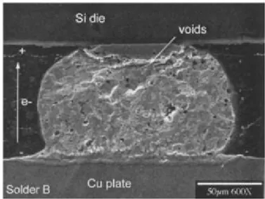
Fig. 6 Voids occurred at cathode side.7
Fig. 7 Smulation of temperature distribution under 1.0A (a) the solder joint (b) Temperature as a function of distance from Al trace to Cu plate Fig. 8 (a) Cross-sectional view of current density distribution in solder joint (b) Corresponding cross-sectional view for temperature distribution. Fig. 9 Flip chip Package (I)
Fig. 10 Schematic for the solder bump
Fig. 11 (a) Cross-sectional view showing the materials and the dimension of a SnPb bump. (b) Plan-view schematic showing the solder joints with 40-μm-wide Al traces. (c) Plan-view schematic showing the solder joints with 100-μm-wide Al traces. (d) Plan-view schematic showing the solder joints with 100-μm-wide Al traces for the investigation of length effect on electromigration.
Fig. 12 (a) Infrared microscope
(b) Infrared microscope schematic diagram for experimental setup, in which the Si side faced the infrared microscope.
vii
Fig. 14 Cross-sectional schematic diagram of the samples used in this study. (package II) Fig. 15 Flip-chip package with meshization.
Fig. 16 (a) Cross-sectional schematic of the layout design. The Al trace connected all the four solder bumps together.
(b) Schematic structure for the solder bump used in this study..
Fig. 17 (a) Temperature distribution in the package before current stressing, showing a uniform temperature in the package.
(b) Radiance image for the same location in (a). Circuit of the Al trace can be clearly observed.
(c) Temperature distribution in the Al trace measured by the IR microscope when powered by 0.59 A
(d) Enlarged image for the temperature distribution in one of the solder joints in (a). (e) Temperature profile along the white line in 16(d).
Fig. 18 (a) The temperature distribution of a bump. A hot spot exist at the entrance points of the Al trace into the solder at the passivation opening.
(b) The temperature distribution in the solder bump. the average temperature in the solder bump was obtained by averaging the temperatures in a square of 70 μm × 70 μm in the center of the solder.
Fig. 19 (a) Simulated temperature distribution in the stressing circuit when powered by 0.59 A. The distribution matched the experimental data in Figure 18(a).
viii
entrance point of the Al traces.
Fig. 20 (a) depicts the temperature in the hot spot and the average temperature in the solder as a function of applied current up to 0.8 A.
(b) vertical and horizontal thermal gradients as functions of the applied current. Fig. 21 (a) Radiant IR image showing the bump B1 in Fig. 9(c). The Al pad,
underfill, and solder can been observed clearly.
(b) Uniform temperature distribution in the Al trace and in the Al pad before current stressing. The average temperature in the Al pad was obtained by averaging the temperatures in the 40 μm × 40μm square. The temperature distribution when it was applied by (c) 0.4 A, (d) 0.6 A, (e) 0.8 A, and (f) 1.0 A currents.
Fig. 22 The temperatures in the Al pad of the bump B1 as a function of applied currents up to 1.0 A for the three stressing setups
Fig. 23 Measured temperatures in the Al pads above the four bumps in 1(c) when the electron flow was (a) from bump B1 to bump B4 (b) from bump B2 to bump B3, (c) from bump B1 to bump B2 under 0.8 A.
Fig. 24 The temperatures in the far left bumps as a function of applied currents for the solder joints with 40-μm-wide and 100-μm-wide Al traces
Fig. 25 One-dimensional lumped model
ix
current for the solder with the 2550-μm-long Al trace in Figure 21..
Fig. 27 (a) Plan-view x-ray image of the joint before current stressing. The UBM and passivation openings were labeled by the dotted white circles.
(b) X-ray image of the same joint after current stressing. The void was enclosed by the white line.
(c) X-ray image of the same joint after being polished laterally to middle of the joint.
(d) Cross-sectional SEM image of the joint in (c). A void formed near the entrance of the Al trace.
Fig. 28 Plan-view x-ray images of the joint after stressing for (a) 37.8 h. (b) 110.2 h.
(c) 177.8 h. and (d) 384.0 h. The position of the Al trace was labeled by the dotted lines in the Figures.
Fig. 29 The corresponding cross-sectional SEM images of the joint in Figures 28(a) through 28(d)
Fig. 30 (a) Plot of depletion area as a function of stressing time.
(b) Plot of void growth velocity against stressing time for the five samples. The depletion percentage of UBM opening for each sample was also shown in the Figure.
Fig. 31 Plan-view x-ray images of the joint after stressing for (a) 0 h. (b) 50.0 h. (c) 941.4h (d) 1087.9 h.
x
Fig. 32 IR images of the joint after stressing for (a) 0 h. (b) 50.0 h. (c) 941.4 h (d) 1087.9 h
Fig. 33 The average temperature increase for the five current stressing time Fig. 34 (a) IR image for the hot spot was found by 1087.9 h
(b) X-ray image of the samejoint after current stressing. The hot spot was labeled. (c) Cross-sectional SEM image of the joint in (c).
xi
List of Tables
Table I. Thermal conductivities, electrical resistivities, and temperature coefficients of resistivity for the materials used in the simulation model.
Table II. Failure time of the solder joints with various lengths of Al traces under current stressing.
Table III. Thermal resistance and material properties used in the lumped thermal resistance model.
- 1 -
Chapter I Introduction
1.1 Flip chip technology
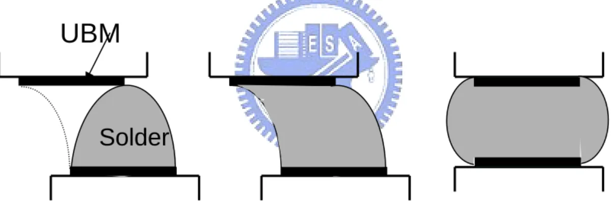
To meet the miniaturization trend for portable devices, flip chip technology has been adopted for high-density packaging due to its excellent electrical performance and better heat dissipation ability.[1] Area arrays of solder bumps are fabricated on a silicon chip to achieve high input/output (I/O) pin count. Flip Chip Technology was developed by IBM since the end of 60`s. The so-called C4(Controlled Collapse Chip Connection) technology deposited solder bumps on wettable metal terminals on the chip and a matching footprint of solder wettable terminals on the substrate as shown in Figure 1 and Figure 2 [2]. Then the chip was aligned on the ceramic substrate. IBM's C4 used evaporation for deposition of high-lead (95%) solder through a metal mask. The main purpose was to provide differential melting temperatures; the board-level 63% Sn-37% Pb solder melts at 183°C while the flip-chip solder melts at 315°C. Flip chip technology provides high input/output (I/O) pin counts for the package. It also has two important advantages, one is the solder bumps reflowed in the same time for all the contact, the other is self-alignment process as shown in Figure 3. Because of melting solder surface tension and the Under Bump Metallurgy good wetting ability of solder and Under Bump Metallurgy(UBM) layers. Thousands of contacts aligned simultaneously under reflow process. Today flip-chips Technology is widely used for high performance electronic
- 2 -
- 3 -
- 4 -
Figure 3.
Solder self-alignment process
Solder
UBM
- 5 -
1.2 Electromigration theory
Electromigration is a combination of thermal an electrical effects on mass motion. It is a phenomenon of mass transport by the electric field and charge carriers. Electromigration is a mass transport driven by an electric field. The direction of mass transport is the same as that of electron flow for metals. The phenomenon of electromigration can be illustrated by the response of short conducting lines under a high current density. Figure 4 shows
electromigration of Al line, which is a typical Blech structure.[3] Electromigration occurs and leads to extrusion at the anode and voids at the cathode.
- 6 -
The driving force for electromigration consists of the “electron wind force” and the “electrostatic field force”. The electron wind force refers to the effect of momentum exchange between the moving electrons and the ionic atoms when an electrical current is applied to the specimens [4]. The electron flow might act as a “frictional” force on the diffusing atoms. The “frictional” force is commonly called “electron wind force.”
When a thin film stripe is stressed under a high current density, the electrons would hit the atoms at the cathode side and the momentum would be exchanged between electrons and diffusing atoms. This phenomenon is formed by the interaction of two different types of force:
1. Coulombic force: the force between the electrostatic force and metal ion, when an external electric field is applied.
2. Electron wind force: the force made by the momentum exchange between electrons and diffusing atoms.
The atomic diffusion flux in a solid can be written as:[3]
∑
+
∂
∂
−
=
i i iF
CM
X
C
D
J
(1.1)Where the first term represents the chemical potential gradient, and the second term represents the sum of different forces. For a pure metal, there is no chemical potential gradient between the atoms, so the first term is zero. The second term is what we discussed above, the combination of direct action of the electrostatic field and the momentum exchange of electrons and diffusing atoms. For simplicity, the second term can be written as: [3]
wd el i i i
F
F
F
CM
=
+
∑
(1.2)By comparing the magnitude between the electrostatic field force and the electron wind force, we can know that the electron wind force is much bigger than the electrostatic field force so that the atoms would be pushed from the cathode side to the anode side. Besides, the
- 7 -
dominative term Fwd can be written as: [5]
e
EZ
F
wd=
*
(1.3)where E is the electric field, Z* is the effective charge number. Z* is a parameter to express how the atoms would migrate when they are effected by electromigration. So, the Z* value would vary from different metal atoms. Then, we can combine equation (2.1) and (2.2): [3]
wd
CMF
J
=
(1.4)where M is the mobility of the atoms and C is the atomic concentration. By using the Einstein equation, the mobility can be written as:
KT
D
M
=
(1.5)where D is the diffusivity, K is the Boltzmann’s constant, T is the absolute temperature. Now, we can combine equation (1.3), (1.4) and (1.5), so we can obtain the following equation:
eE
Z
KT
D
C
CMF
J
em=
wd=
*
(1.6)- 8 -
1.3 Electromigration in flip chip solder joint
To meet the miniaturization trend for portable devices, flip chip technology has been adopted for high-density packaging due to its excellent electrical performance and better heat dissipation ability.[6] As the required performance in microelectronics devices becomes higher, the design rule requires that the current in each bump should be 0.2 A, and it is expected to increase to 0.4 A in the near future.[7] Therefore, electromigration has become an important reliability issue.[8]
1.3.1 Joule heating effect
Joule heating effect is that the electrons moving through a metal, the electrical energy converted into thermal energy. The heating power can be expressed as
P = I2R = j2ρV (2.1)
where P is Joule heating power, I is the current, R is the resistance, j is the local current density, V is the volume of the material, and ρ is the resistivity. The product of I2
R is the total
heating power, whereas j2ρis the heating power per unit volume.
During the electromigration test, the applied current may be as high as 2.0 A, and thus Joule heating effect in the solder bumps becomes significant.[9] Furthermore, the total length of the Al trace is typically few hundreds to few thousands microns, which corresponds to a resistance of approximately few hundreds milli-ohms or few ohms. On the other hand, the resistances of the solder bumps and the Cu trace in the substrate are relatively low, typically in
- 9 -
the order of few or tens of milli-ohms. The major heat source for the solder joints is the Al trace.[10] Hence, the temperature in the bumps during testing may be much higher than that of the ambient due to Joule heating, and may affect the mean-time-to-failure (MTTF) analysis, as delineated by Black’s equation: [11]
) k T Q ( e x p n j A MTTF = 1 (2.2)
where A is constant, j is the current density, n is a model parameter for current density, Q is the activation energy, k is the Boltzmann’s constant, and T is the average bump temperature. It is noteworthy that the MTTF decreases exponentially with the stressing temperature. Wu et al. [12] conducted electromigration test for SnPb solder bumps, and found that the MTTF decreased from 711 hours to 84 hours when the testing temperature increased from 125 °C to 150 °C at 5.0 × 10³ A/cm2, whereas the MTTF decreased from 277 hours to 84 hours as the
current density increased from 2.5 × 10³ A/cm2 to 5.0 × 10³ A/cm2 at 150 °C. Therefore, the
- 10 -
1.3.2 Current crowding effect
In previous work published by Liang et al.[13], current density distribution in a solder joint was thoroughly studied by a three-dimensional finite element simulation. It was found that the maximum current density in a solder bump can be much higher than the average one that was previously projected. It locates itself near the solder/underbump metallization (UBM)
interface, which serves as a vacancy flux divergence plane and favors electromigration occurring at that location. Consequently, the solder joint is more prone to electromigration. The cause of such locally high current density is a result of the current crowding effect. Current crowding occurring in the solder joints is due to the current flow experiencing a dramatic geometrical and resistance transition from the thin on-chip metal line to the solder bump. Because the cross-section of the Al trace on the chip side is about two orders smaller than that of the solder joints, the majority of the current will tend to gather near the Al/UBM entrance point to enter the solder bump instead of spreading uniformly across the opening before entering the bump. The materials near the entrance point experience a current density of about one order of magnitude higher than the average value. Current crowding plays a critical role in the electromigration failure of the solder joints.[13]
- 11 -
1.3.3 Thermomigration
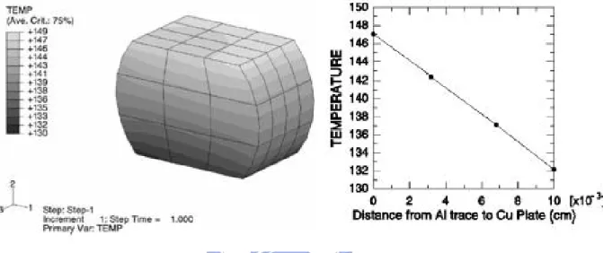
Thermomigration is the atom movement due to temperature gradient.[14,15] As the required performance in microelectronic density increases, the design rule of packaging requires that some of the power bumps may need to carry 0.2 to 0.4 A. Therefore, Joule heating effect in the solder bumps become an important issue. Furthermore, to meet the need for increased miniaturization of portable devices, the dimension and the pitch of the solder bumps continues to shrink, causing the Joule heating effect to be even more serious. Roush found that the thermal gradient is as higher as 1200°C/cm in Pb-In bump, and Pb atoms moved from hot end to cold end in 1982.[16]。Ye at al. stressed the SnPb solder under 1.3 × 10⁵ A/cm2 (1A) for 16 h. The found voids occurred at both anode and cathode side as shown in Figure 5 and Figure 6. They performed a simulation for the temperature distribution, and found the thermal gradient was as high as 1500 °C/cm in a SnPb solder bump when it was stressed by 1.0 A as shown in Figure 7. However, there is still no experimental data to verify the temperature in the bump because the solder joints are completely surrounded by a chip, a substrate and underfill, so no direct temperature measurement can be made to investigate the Joule heating effect inside the solder joints. [17]
- 12 -
Figure 5. Voids occurred at anode side.
- 13 -
Figure 7. Smulation of temperature distribution under 1.0A (a) the solder joint (b) temperature as a function of distance from Al trace to Cu plate
- 14 -
1.3.4 Void formation in flip chip solder joint during electromigration
The pitch of solder bumps has decreased rapidly, in turn the contact area of the solder bumps and the diameter of under bump metallization (UBM) decrease rapidly too. On the other hand, the operation current for the bumps keeps increasing, resulting in a dramatic rise of the current density in the solder bump. [16-18] Tu et al. stressed the SnPb solder with Al/Ni(V)/Cu UBM under 1.90、2.25、2.75 × 10⁴A/cm2 . The voltage was recorded in the same time. They found that once the void was formed and propagated toward the rest of UBM at the interface of Si chip and SnPb solder, dramatic rise of electrical resistance occurred.[16] Brandenburg and Yeh reported the observation of electromigration failure in flip chip eutectic SnPb solder joints stressed under 8x10³ A/cm2 at 150 for a few hundred ℃ hours. [8] The important findings are void formation at the cathode and Pb accumulation at the anode of the solder joint.
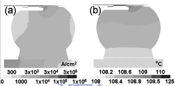
Redistribution of current density and temperature due to void formation in flip-chip solder joints during electromigration was investigated using three-dimensional thermo-electrical coupled modeling, in which the current density and temperature redistribution were simulated at different stages of void growth for solder joints with thin-film UBM. Liang et al. found that after the void formation near the entrance point of Al trace, the current may propagate through the UBM layer to the periphery of the solder joint, leading to the void formation in the
- 15 -
as shown in Figure 8.[25] In addition, the temperature of the solder did not rise significantly until 95% of the contact opening was eclipsed by the propagating void. It is proposed that current redistribution is the main reason accounting for void formation and propagation, especially the propagation into the low current density region below the contact passivation. It is found that UBM provided a conducting path for current to go below the passivation, and it directed the current to the periphery of the solder joint, which is in agreement with the experimental observation of void formation in those regions. Increase in temperature due to void formation was not significant since the major heat source was the Al trace and the applied current was as low as 0.28 A. However, there is also no experimental data to verify temperature redistribution due to void formation in real flip-chip solder bumps. We will discuss that in later chapters.
- 16 -
Figure 8 (a) Cross-sectional view of current density distribution in solder joint (b) Corresponding cross-sectional view for temperature
- 17 -
1.4 Motivation
Since electromigration is the result of a combination of thermal and electrical effects on mass motion, the Joule heating effect must be addressed to provide better understanding of the electromigration behavior. The current used for typical accelerated electromigration tests ranges from 0.5 A to 2.2 A. Although whether a hot spot exists at the current crowding region is of interest, only a few studies have addressed the Joule heating effect in solder joints.[9, 10, 19] Furthermore, the total length of the Al trace is typically few hundreds to few thousands microns, which corresponds to a resistance of approximately few hundreds milli-ohms or few ohms. On the other hand, the resistances of the solder bumps and the Cu trace in the substrate are relatively low, typically in the order of few or tens of milli-ohms. The major heat source for the solder joints is the Al trace.[10] Hence, the temperature in the bumps during testing may be much higher than that of the ambient due to Joule heating, and may affect the mean-time-to-failure (MTTF) analysis, as delineated by Black’s equation (2.2):[11]
It is noteworthy that the MTTF decreases exponentially with the stressing temperature. Wu et
al.8 conducted electromigration test for SnPb solder bumps, and found that the MTTF
decreased from 711 hours to 84 hours when the testing temperature increased from 125 °C to 150 °C at 5.0 × 10³ A/cm2, whereas the MTTF decreased from 277 hours to 84 hours as the
current density increased from 2.5 × 10³ A/cm2 to 5.0 × 10³ A/cm2 at 150 °C. Therefore, the
- 18 -
Ye at al. performed a simulation for the temperature distribution, and found the thermal gradient was as high as 1500 °C/cm in a SnPb solder bump when it was stressed by 1.0 A. However, there is still no experimental data to verify the temperature in the bump because the solder joints are completely surrounded by a chip, a substrate and underfill, so no direct temperature measurement can be made to investigate the Joule heating effect inside the solder joints. For this study, we used thermal infrared (IR) microscopy to measure the temperature distribution in the Al trace at various stressing conditions. Based on the experimental data, we constructed a finite element model to simulate the temperature distribution inside the solder bump during current stressing. Therefore, this study provides deeper understanding of the Joule heating effect inside the flip-chip solder joints during current stressing.
During electromigration, voids nucleate in the solder bump near the point of entry of the electron flow, where serious current crowding and flux divergence occur.[20,21] In previous studies, void formation and propagation were observed by cross-sectional scanning electron microscope (SEM). Therefore, only the length and the depth of the void at those specific cross-sections can be observed. However, the location where voids nucleate, the shape of voids, as well as how voids propagate in the UBM opening remains unclear. In addition, the propagation velocities of voids at different stages have not been measured. X-ray microscopy has been used to study formation of voids in Cu interconnects during electromigration.[22] Since the size of voids formed in Cu interconnects is in submicron range, synchrotron
- 19 -
radiation x-ray is needed. For flip-chip solder joints, the voids are of a much larger dimension, typically ranging from few microns to tens of microns. Thus, a laboratory-based x-ray
microscope appears to be sufficient for the investigation of void nucleation and propagation in solder joints during electromigration. Nevertheless, it has not been applied to solder joints.
- 20 -
Chapter II Experimental
2.1 Fabrication of clip chip packages (I)
The fabrication procedure for the SnAg bumps were prepared as follows: A SnAg3.5 solder paste was printed and deposited on the UBM pad of the chip. The chip was reflowed in a nitrogen atmosphere oven at the 250°C peak temperature and remained above the liquid temperature for approximately 60 s. Then, the bumped die sample was prepared after sawing. Afterward, the bumped die was mounted on a BT substrate, on which the SnAg3.5 solder paste was printed through a metal stencil printing on the metallization pads of the substrate. Then, the flip-chip sample was reflowed for the second time in a nitrogen atmosphere oven at the 250°C peak temperature for approximately 60 s. The flip-chip joints were formed after the second reflow. Afterward, the flip-chip package was under filled as shown in Figure 9.
Figure 10 shows the schematic for the solder bump. The thickness of the Si chip was 300 μm. The under-bump-metallization (UBM) consisted of 0.7 μm Cu, 0.3 μm Cr-Cu, and 0.1 μm Ti. It is assumed that a layer-type Cu6Sn5 intermetallic compound (IMC) of 1.4 μm thick
grew in the interface of the UBM and the solder, whereas a layer-typeNi3Sn4 IMC of 1.0 μm
thick formed in the interface of the pad metallization and the solder in the substrate side. The UBM and passivation openings were 120 μm and 85 μm in diameter, respectively. The Al trace on the chip side was 34 μm wide and 1.5 μm thick. BT substrate was employed for the flip chip package.
- 21 -
- 22 -
- 23 -
2.2 Fabrication of flip chip packages (II)
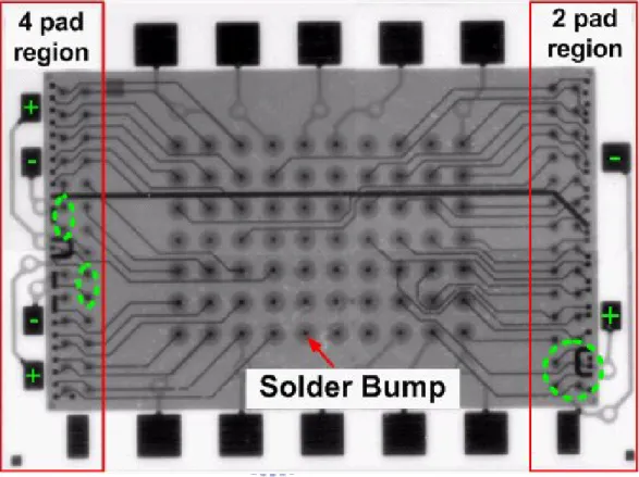
To analyze the effect of Al-trace dimension on electromigration of flip-chip solder joints, another flip chip package was prepared. The dimension of the flip-chip joint used in this study is shown in Figure 11(a) schematically. The under bump metallization (UBM) was Ti/Cu/Cu/Ni. A titanium layer of 0.1 μm was sputtered on the oxidized Si wafer and acted as an adhesion layer. Copper (0.5 μm) was then sputtered on the Ti layer and served as a seed layer for the subsequent electroplating process. Then a 5-μm Cu and a 3-μm Ni layers were electroplated on the Ti/Cu layers. Photolithography was applied to define the UBM opening. Afterwards, the UBM opening was formed by wet etching process. Due to the fast etching of Cu, the diameter of Cu UBM was smaller than that of the Ni UBM, as shown in Figure 11(a). The passivation and UBM openings are 110 µm and 120 µm in diameter, respectively. Eutectic SnPb solder was electroplated onto the UBM, followed by reflowing in an infrared oven at 220 for about 1 minute. The solder bumps were jointed to FR4 substrates. The pad ℃ metallization consisted of 1-μm Au and 5-μm electroless Ni layers. The dimension of the pad opening was 300 μm in diameter. The dimension of the Si chip was 5.35 mm long, 4.35 mm wide, and 250 μm thick, whereas the dimension of the FR4 substrate was 5.35 mm long, 4.35 mm wide, and 250 μm thick. Two different layouts of Al traces were fabricated: one was 40 μm wide and 1.5 μm thick as shown in Fig. 11(b); the other was 100 μm wide and 1.5 μm thick, as shown in Fig. 11(c). The four bumps in Fig. 11(d) were labeled as B1 through B4, and the three Al traces were labeled as T1 through T3. The pitch for both test samples was 850 μm. The non-solder mask process was adopted.
- 24 -
Figure 11(a) Cross-sectional view showing the materials and the dimension of a SnPb bump.
Figure 11(b) Plan-view schematic showing the solder joints with 40-μm-wide Al traces.
Figure 11(c) Plan-view schematic showing the solder joints with 100-μm-wide Al traces.
Figure 11(d) Plan-view schematic showing the solder joints with 100-μm-wide Al traces for the investigation of length effect on electromigration.
- 25 -
2.3 Temperature measurement by infrared microscopy
An Infrared microscope(Quantum Focus Instrument) as shown in Figure 12(a) was
employed to measure the temperature in the Al trace during current stressing. The temperature distribution inside the bumps when powered by electric current was detected by a thermal infrared microscope, which has the resolution of 0.1 °C in temperature sensitivity and 2.8 μm in spatial resolution. The current stressing of the specimen was performed on a hot plate in ambient air, which has heating capacity up to 120℃. Prior to the current stressing, the emissivity of the specimen was calibrated at 100 °C. After the calibration, the bumps were powered by a desired current stressing condition. Then, temperature measurement was performed to record the temperature distribution after the temperature reached a steady state. Figure 12(b) shows the schematic diagram for experimental setup, in which the Si side faced the infrared microscope.Since the 250 μm Si is transparent to infrared,the corresponding penetration depth is larger than 2m and much larger than the thickness of the silicon wafer. Therefore, the absorption can be ignored.[28] The temperature distribution in the Al traces and in the Al pad directly above the solder bumps during current stressing can be measured.
- 26 - 1. Cooling chamber 2. CCD Sensor 3. Cantilever -X 4. Cantilever -Y 5. Cantilever -Z 6. Camera 7. IR detector 8. Heating apparatus 9. Heater 10. Heater stage 11. Stage Figure 12(a) Infrared microscope
- 27 -
Figure 12(b) Infrared microscope schematic diagram for experimental setup, in which the Si side faced the infrared microscope.
- 28 -
2.4 Microstructure examination
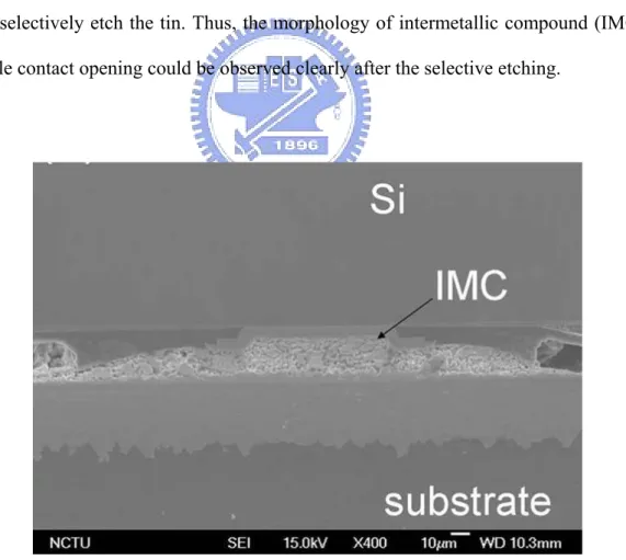
A JEOL 6500 scanning electron microscope (SEM) and energy dispersive spectroscopy (EDS) were used to observe the microstructure and composition of the solder joints in the flip chip package. The cross-sectional samples were prepared by polishing laterally until the contact opening was visible. Figure 13 shows the cross-sectional SEM image for the fabricated samples. Due to the large opening in the substrate side, the bump height was as small as 25 μm. Both the electroplated and elctroless Ni layers reacted with the solder to form Ni3Sn4 intermetallic compounds (IMCs), and the average thickness of the IMCs was 1 μm.
SEM was also employed to examine the voids in the cross-section of the solder bumps. Then, an etching solution consisting of glycerin, nitric acid and acetic acid at ratio of 1 : 1 : 1, was used to selectively etch the tin. Thus, the morphology of intermetallic compound (IMC) and the whole contact opening could be observed clearly after the selective etching.
- 29 -
2.5 X-ray microscope
In this study, void formation during electromigration was monitored by an x-ray
microscope. A DAGE XL-6500 x-ray microscope with the Si side facing the x-ray detector, which has 2 μm in spatial resolution. The corresponding current density was 6.5×10³ A/cm2.
The operation voltage was set at 95 kV in this study. Since voids form in the bump with electron flow from the chip side to the substrate side, only the bumps with this stressing direction were examined. The solder joints were stressed by 0.8 A at 150°C for a desired time.
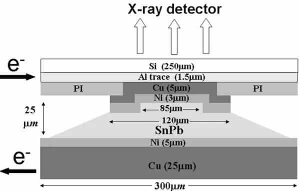
Figure 14 shows the cross-sectional schematic for the solder joint used in this study. The dimension of the Al trace was 1.5 μm thick and 100 μm wide, while the dimension of the Cu lines on the substrate was 25 μm thick and 100 μm wide. The UBM consists of 0.1-μm Ti, 5-μm Cu, and 3-μm Ni layers. The diameter of the UBM and the passivation openings was 120 μm and 85 μm, respectively. Electroplated SnPb solder bumps were mounted on a FR4 substrate to form flip-chip joints. Non-solder-mask-defined process was used in this structure. The dimension of the Cu pad opening was 300 μm in diameter. Owing to the large opening in the substrate side, the bump height was as small as 25 μm. With the low bump height, the voids in the solder bump would be much clearly seen in an x-ray microscope.
- 30 -
- 31 -
2.6 3-D thermo-electrical simulation by finite element analysis
On the basis of the experimental results, a three-dimensional (3-D) simulation was carried out by finite element analysis. The schematic diagram for the package is shown in Figure 12(b). Two solder bumps had electrical current applied through the circuit shown in the Figure. The electrical and thermal resistivities for the materials used in this modeling are listed in Table I. The effect of temperature coefficient of resistiviy (TCR) was considered, and the TCR values for the metals are also listed in Table I. In addition, 3-D coupled thermal-electric simulation was conducted to predict the steady state temperature distribution using the ANSYS software package developed by ANSYS, Inc. The model used in this study was a SOLID69 8-node hexahedral coupled field element. All the boundary conditions followed the experiment setup, shown in Figure 12(b). The whole flip chip package with meshization is illustrated in Figure 15. The area of the Si chip was 10.0 mm × 6.0 mm and the thickness was 290 μm, whereas the BT (Bismaleimide Triazine) substrate was 4.75 mm wide, 7 mm long, and 350 μm thick.
- 32 -
Table I. Thermal conductivities, electrical resistivities, and temperature coefficients of resistivity for the materials used in the simulation model.
Material Thermal conductivity
(W/m-°C) Resistivity(μΩ-cm) at 20°C TCR (10-3K-1) Silicon 147.00 -- -- Al trace 238.00 2.70 4.2 UBM(Ti+Cr/Cu+Cu) 147.61 5.83 4.9 SnAg3.5 33.00 12.3 4.6 Ni 76.00 6.8 6.8 Cu pad 403.00 1.7 4.3 BT (substrate) 0.70 -- -- Underfill 0.55 -- -- Passivation 0.34 -- --
- 33 -
- 34 -
2.7 Bump resistance measured by Kelvin bump probes
In this study, we employed Kelvin bump probes to monitor the bump resistance change during electromigration. A bump resistance change as small as 0.1 mΩ could be detected. The corresponding void formation causing the increase in bump resistance can be examined at different stages. We have designed and fabricated Kelvin probes for flip-chip eutectic SnPb solder joints. Figure 16(a) shows the plan-view schematic for the structure. The test structure consisted of four bumps, in which an Al trace connected all of them together. The four bumps were labeled as Bump 1 though Bump 4, respectively. The dimension of the Al trace was 1.5 μm thick and 100 μm wide. The pitch for the solder joints was 1 mm. Six Cu lines on the FR4 substrate connected to the four bumps, and they were labeled as node 1 through 6, as shown in the Figure. The dimension of the Cu lines was 30 μm thick and 100 μm wide. Through these six Cu lines, various experimental setups can be performed to measure the bump resistance for Bump 2 or Bump 3, or the resistance for the middle segment of the Al trace. In this study, the current was applied through nodes 3 and 4, i.e. electrons flowing from the chip side to the substrate for Bump 2, and the opposite direction for Bump 3, as illustrated in Figure 16(b). The voltage change in the Bump 2 was monitored through nodes 1 and 2, whereas the voltage change in the Bump 3 was supervised though nodes 5 and 6. Therefore,
- 35 -
the change in bump resistance during electromigration for the two bumps with opposite direction of electron flow can be monitored simultaneously. In general, voids initiate in the chip side of the Bump 2 due to serious current crowding effect. Hence, we will present the results for Bump 2 only in this study. The power supply used in this measurement was Keitheley 2400, which has a 0.1 μV resolution in voltage measurement. The error in measuring resistance in this study was estimated to be 1 to 10 μΩ.
- 36 -
Figure 16 (a) Cross-sectional schematic of the layout design. The Al trace connected all the four solder bumps together. (b) Schematic structure for the solder bump used in this study.
- 37 -
Chapter III Results and Discussion
3.1 Temperature measurement of Al-trace in flip chip solder joints under
current stressing (I)
In this study, we used thermal infrared (IR) microscopy to measure the temperature
distribution in the Al trace at various stressing conditions. Temperature increase in the Al trace due to current stressing was measured from the whole bumps. Before the current stressing, calibration was performed on a hot plate maintained at 70 °C. The temperature distribution without current stressing is shown in Figure 17(a). The circuit of the Al trace can barely be seen since the Si substrate is transparent to infrared radiation. The temperature was calibrated to 70 °C. Furthermore, the circuit can be clearly observed in the radiant mode, as shown in Figure 17(b). The Al trace, UBM and passivation openings are labeled in the Figure. Figure 17 (c) shows the temperature increase for the Al trace in the package when stressed by 0.59 A at the ambient temperature of 70 °C. The current path is indicated by two of the arrows in the Figure. There were two solder bumps located directly below the two circular Al pads/UBMs, as labeled in the Figure. It is noteworthy that the Al trace has much higher temperature than the circular Al pads, which were directly connected to the UBM and the solder bumps. The maximum temperature was as high as 134 °C, which occurred approximately at the middle of the Al trace, whereas the temperature was only about 105 °C for the Al pads above the solder bumps. It is expected that the solder near the circular Al pad had the same temperature as the
- 38 -
circular Al pad, since these metals are good heat conductors and the total thickness of the Al and the UBM layer was less than 3 μm, as shown in Figure 17(a). The solder served as a heat sink, and thus the temperature in the circular Al pad was much lower than that in the isolated Al trace. Figure 17(d) shows the enlarged image of one of the bumps in Figure 17(c). The inner circle represents the passivation opening, whereas the outer circle corresponds to the UBM opening of the solder joint.
Furthermore, whether a hot spot exists inside the solder is of interest for electromigration study. The solder directly below the Al trace near the entrance point may have higher temperature than the rest of the solder. Figure 17(e) illustrates the temperature profile along the 75 μm long dashed line in Figure 17(d). The points A and B in Fig. 17(e) represent the edges of the UBM and the passivation openings, respectively. The temperatures at points A and B were approximately 118.2 °C and 109.7 °C, respectively, which are much higher than the average temperature of 105.2 °C in the Al pad. The average temperature was calculated by averaging the temperatures in a 10 μm × 10 μm square in the center of the passivation
opening. Since there was solder below this segment of the Al trace, the temperature in this solder may be higher than the rest of the solder. In addition, there is a thermal gradient since the temperature at the Al pad near the entrance of the Al trace was higher than that at the opposite end. The gradient in this junction was as high as 1700 °C/cm.
- 39 -
Figure 17(a) Temperature distribution in the package before current stressing, showing a uniform temperature in the package.
- 40 -
Figure 17(b) Radiance image for the same location in (a). Circuit of the Al trace can be clearly observed.
- 41 -
Figure 17(c) Temperature distribution in the Al trace measured by the IR microscope when powered by 0.59 A
- 42 -
- 43 -
- 44 -
3.2 Distribution of current density and temperature in flip chip solder
joints
Figure 18(a) shows the simulated temperature distribution in the Al trace and in the solder joints when stressed by 0.59 A. The simulation results fit the experimental results very well. The temperature distribution inside the solder in one of the cross sections near the entrance of the Al trace is shown in Figure 18(b). As for the temperature distribution in the solder bump, Figure 18(a) shows the distribution in the solder bump only, in which the Al pad, UBM, IMC layer, and the BT substrate were excluded. It is clear that there is a hot spot near the entrance point of the Al trace, as indicated by the arrow in the Figure. Figure 18(b) shows the
distribution in the center cross-section of the bump, in which the temperature distribution across the solder bump can be clearly seen. The average value was obtained by averaging the values in the area of 70×70 μm2, as labeled in the Figure. The occurrence of the hot spot may
be mainly attributed to the local Joule heating effect, since there is serious current crowding effect in the hot-spot region.[16] This gradient play important role in the thermomigration in the solder joints.[18, 24]
- 45 -
Figure 18 (a) The temperature distribution of a bump. A hot spot exist at the entrance points of the Al trace into the solder at the passivation opening.
- 46 -
Figure 18 (b) The temperature distribution in the solder bump. the average temperature in the solder bump was obtained by averaging the temperatures in a square of 70 μm × 70 μm in the center of the solder.
- 47 -
Figure 19(a) shows the simulated temperature distribution in the Al trace and in the solder joints when stressed by 0.59 A. The simulation results fit the experimental results very well. The temperature distribution inside the solder in one of the cross sections near the entrance of the Al trace is shown in Fig. 19(b). A hot spot existed in the solder adjacent to the entrance points of the Al trace into the solder at the passivation opening. The temperature at the spot was 95.6 °C, which was 4.5 °C higher than the average value in the solder. The temperature on the chip side was higher than that on the substrate side. In addition, the vertical thermal gradient was measured to be 276 °C/cm, whereas the horizontal thermal gradient was
calculated to be 634 °C/cm at this stressing condition. The thermal gradient is denoted in this letter as the subtraction of the temperature in the hot spot by the temperature at the opposite end of the solder, then divided by the distance between the two locations. Under this stressing condition, the current density in the Al trace was 1.1 x 10⁶ A/cm2. The average current density
in the joint was 5.2 x 10³ A/cm2 based on the UBM opening. In the hot spot, the maximum current density was 1.7 x 10⁵ A/cm2, whereas the average current density involved in a volume of 5 μm x 5 μm x 5 μm was estimated to be 1.4 x 10⁵ A/cm2.
The Joule heating effect was also inspected at various applied currents. Figure 20(a) depicts the temperature in the hot spot and the average temperature in the solder as a function of applied current up to 0.8 A. Both of them increased rapidly with the increase of applied current. The difference in these two temperatures increases as the applied current increases,
- 48 -
and it may be as high as 9.4 °C when stressed by 0.8 A. Figure 20(b) shows the vertical and horizontal thermal gradients as functions of the applied current. They also increase with the increase in stressing current. Moreover, the horizontal thermal gradient rose more quickly than the vertical one, reaching 1320 °C/cm under the stressing of 0.8 A.
- 49 -
Figure 19 (a) Simulated temperature distribution in the stressing circuit when powered by 0.59 A. The distribution matched the experimental data in Figure 18(a).
- 50 -
Figure 19 (b) Temperature distribution inside the solder bump. A hot spot was found in the entrance point of the Al traces.
- 51 -
Figure 20 (a) Depicts the temperature in the hot spot and the average temperature in the solder as a function of applied current up to 0.8 A.
- 52 -
- 53 -
3.2.1 Joule heating effect in flip chip solder joints
3.2.1.1 Hot spot in solder joint during electromigration
The existence of the hot spot may be attributed to two reasons. First, it may be due to the local Joule heating inside the solder itself. The heating power can be expressed as (2.1). In our simulation model, the total resistance of the Al trace was about 900 mΩ, and the resistance of the solder bump was about 10 mΩ. Therefore, the Al trace generated most of the heat. Due to the serious current crowding in the solder joint, the current density in the vicinity of the Al entrance into the solder joint is typically one to two orders higher than the average value,[9, 18, 19] causing local Joule heating there. Second, the Al trace has higher Joule heating effect, and the hot spot was close to the Al trace. At lower stressing current, the hot spot is not obvious because there is less heat generation. However, it became more
pronounced as the applied current increased due to large heat generation and difficulty in heat dissipation. The solder in the hot spot was the most vulnerable part in the solder joint during electromigration testing, since it may experience much larger electron wind force due to the higher current density and the higher diffusivity owing to the higher temperature as well as it’s low melting point. Hence, voids start to form at this spot.
- 54 -
3.3 Temperature measurement of Al-trace with various dimensions in
flip chip solder joints under current stressing (II)
Electromigration test was performed for the above solder joints to examine the effect of Joule heating on electromigration failure time. For the solder joints with the 40-μm-wide Al trace, they failed instantly at and above 0.6 A at 100 °C. The SnPb solder may be melted at these stressing conditions. Nevertheless, the failure time was 18 hours when applied by 0.6 A for the solder joints with the 100-μm-wide Al trace in Figure 11(b). For the solder joints with the 100-μm-wide Al trace in Figure 11(d), the electromigration failure time was 35 hours when a current of 1.0 A was applied through bumps B1 and B4 at 100 °C. The corresponding current density was 7.1 × 10³ A/cm2 on the basis of the UBM opening. However, when the
same amount of current was applied through bumps B1 and B3, the failure time was 1700 hours. When the current was applied through Bump B1 and B2, the joints did not fail after 3000 hours. Therefore, the dimension of the Al-trace has huge effect on the electromigration failure time. Table II summarizes the above results.
- 55 -
Table II. Failure time of the solder joints with various lengths of Al traces under current stressing. Al-trace dimension 850-μm-long, 100-μm-wide, 1700-μm-long, 100-μm-wide, 2550-μm-long, 100-μm-wide, 2550-μm-long 40-μm-wide, daisy chains 2550-μm-long 100-μm-wide, daisy chains Applied current 1.0 A 1.0 A 1.0 A 0.6 A 0.6 Failure time > 3000 hr 1700 hrs 35 hrs Failed instantly 18 hrs
- 56 -
Since the current-density distribution was the same for the three stressing conditions for solder joints with 100-μm-wide Al trace, the difference in failure time was mainly attributed to the difference in Joule heating effect. To examine the Joule heating effect in the solder joints, the temperature distribution in the Al trace and in the Al pad was measured using the IR microscope. Figure 21(a) shows the IR radiant image of the bump B1 with a 100-μm wide Al trace shown in Fig. 11(d). The Al trace and Al pad can be clearly observed in the Figure. Figure 21(b) shows the temperature distribution before the current stressing when the package
was placed on a hotplate that was maintained at 100 in air ambient. The temperature ℃
distribution was quite uniform. When the solder joint was stressed by the current, the temperature in the Al trace and in the Al pad can be measured based on the calibration in Figure 21(b). Figure 21(c) to 21(f) show that the temperature increases in the Al pad for the bump B1 in Fig. 11(d) when stressed by 0.4, 0.6, 0.8 and 1.0 A through bumps B1 and B4. In this paper, the average temperature in the Al pad was obtained by averaging the temperatures in a square of 40 μm × 40 μm in the center of the pad, as illustrated by the dotted lines in Fig. 21(b). The average temperature increase due to the current stressing was as high as 65.1 . ℃
Joule heating effect in the solder joints with different lengths of Al traces was investigated using the test structure in Figure 11(d). The current may be applied through bumps B1 and B2, or through bumps B1 and B3, or through bumps B1 and B4. Thus, current flows through Al traces of T1, (T1+T2), and (T1+T2+T3), respectively, for the above three
- 57 -
current-stressing setups. The corresponding lengths of the Al traces are 850 μm, 1700 μm, and 2550μm, respectively. Figure 22 shows the temperatures in the Al pad of the bump B1 as a function of applied currents up to 1.0 A for the three stressing setups. At a lower stressing currents below 0.2 A, there was no obvious difference in temperatures for the three stressing conditions. However, it became more pronounced as the applied current is increased. When stressed by 1.0 A, the temperature in the pad was 119.1 °C, 138.6 °C, and 165.1 °C for the three stressing setups, respectively. The differences are significant in terms of electromigration study. As a consequence, the Joule heating effect was the main reason that caused the above significant difference in electromigration life time under the same current.
During the current stressing, the neighboring bumps without current going through them may also have a temperature increase too. Figure 23(a) shows the temperatures in the four bumps when 0.8 A current was applied through bumps B1 and B4. It is found that the average temperature in the middle two bumps was 137.2 °C, which was higher than those in the two ends, and the difference was only about 2.7 °C. When the same current was applied through bumps B2 and B3, the temperature was about 113.0 °C for bumps B2 and B3, as shown in Fig. 23(b). However, the temperatures in the bumps B1 and B4 were as high as 111.0 °C, although they had no electric current flowing through. It indicates that the neighboring bumps experience almost the same Joule heating as the stressed bumps. Figure 23(c) shows the temperatures in the four bumps when the current was powered through bumps B1 and B2.
- 58 -
The temperatures in the two bumps were about 112.5 °C, whereas it was 110.7 °C in the neighboring Bumps 3 and 4.
On the other hand, the width of the Al trace may affect the Joule heating profoundly in the solder joints at high stressing currents. To investigate the width effect, the current was applied through the far left bump and the far right bump in Figure 11(b), and the same amount of current was applied through the far left bump and the far right bump in Figure 11(c). The temperatures in the Al pad of the far left bumps of the two layouts were measured during the current stressing. For both layouts, the length of Al trace was 2550 μm. The measured resistance values were 1.08 Ω and 2.66 Ω at 100 for the layout with 100℃ -μm-wide and 40-μm-wide Al traces, respectively. Figure 24 shows the temperatures in the far left bumps as a function of applied currents for the solder joints with 40-μm-wide and 100-μm-wide Al traces. When applied 0.2 A current, the temperature difference was only 2.1 °C between the two solder joints. However, it increased up to 20.1 °C at 0.6 A. Therefore, the width of the Al trace also has a significant effect on Joule heating in solder joints.
- 59 -
Figure 21(a) IR radiant image of the bump B1 with a 100-μm wide Al trace shown in Fig. 11(d).
- 60 -
Figure 21(b) The temperature distribution before the current stressing when the package was placed on a hotplate that was maintained at 100 in air ambient.℃
- 61 -
Figure 21(c) The temperature increases in the Al pad for the bump B1 in Fig. 11(d) when stressed by 0.4 A through bumps B1 and B4.
- 62 -
Figure 21(d) The temperature increases in the Al pad for the bump B1 in Fig. 11(d) when stressed by 0.6 A through bumps B1 and B4.
- 63 -
Figure 21(e) The temperature increases in the Al pad for the bump B1 in Fig. 11(d) when stressed by 0.8 A through bumps B1 and B4.
- 64 -
Figure 21(f) The temperature increases in the Al pad for the bump B1 in Fig. 11(d) when stressed by 1 A through bumps B1 and B4.
- 65 -
Figure 22. The temperatures in the Al pad of the bump B1 as a function of applied currents up to 1.0 A for the three stressing setups
- 66 -
Figure 23. Measured temperatures in the Al pads above the four bumps in 1(c) when the electron flow was (a) from bump B1 to bump B4 (b) from bump B2 to bump B3, (c) from bump B1 to bump B2 under 0.8 A.
- 67 -
Figure 24. The temperatures in the far left bumps as a function of applied currents for the solder joints with 40-μm-wide and 100-μm-wide Al traces.
- 68 -
3.3.1 Effect of Al-trace dimension on Joule heating effect on
electromigration
The measured temperature on the Al pad may be close to the temperature of the solder bump located directly below it, since the metals are good heat conductors and the total thickness of both Al and UBM is less than 10 μm. From the analysis by a one-dimensional lumped model as shown in Figure 25, thermal resistance for each layer can be calculated on the basis of the materials properties listed in Table III. The temperature difference between the Al pad and the top layer of solder was estimated to be only 0.5 °C. Therefore, the measured temperatures in the Al pad are quite meaningful, and they could be used to investigate the Joule heating effect in the solder bumps.
The Joule heating effect is larger than expected. The heating power can be expressed as (2.1). In this study the total resistance was 1210 mΩ at 100 for the stressing circuit in ℃ Figure 11(d) when powered through Bumps 1 and 4, in which the resistance of the Al trace weighed 81%. The resistance of a solder bump is only about 5 mΩ,[26] and the rest of the resistance was contributed from the Cu line in the substrate. Consequently, the Al trace was the major heat source to influence the temperature in the solder bumps. Based on the above equation, the plot of temperature increase as a function of the square of the applied current is expected to be linear, because the temperature increase is proportional to the heating power. However, it was higher than the linear relationship. Figure 26 shows the plot of the measured temperature increase against the square of the applied current for the solder with the 2550-μm-long Al trace in Figure 21. The dotted line in the Figure was the tangent line for the fitted curve at zero applied current. It was found that the higher the applied current, the more was the deviation of the temperature from the linear relationship. However, based on Equation
- 69 -
(2), the plot of temperature increase against the square of the applied current should be linear, as shown in the dotted line in Figure 28. The deviation from the linear relationship may be
mainly attributed to the temperature coefficient of resistivity (TCR). During the
electromigration test at elevated temperature, say 100 °C, the resistances of the Al, Cu, and solder increased due to TCR effect. In addition, when high currents are applied, the Joule heating effect raises the temperatures of the Al traces, Cu lines, and solder bumps, causing their resistances even higher. Thus, Equation (2.1) should be modified to account for the
TCR effect. Typically, the TCR can be assumed to be linear and can be expressed as:
)] ( 1 [ ) ( ) (T =ρ T0 × +a T −T0 ρ (3) Where a is the TCR, T is the test temperature, ρ(T) is the resistivity at T °C, and ρ(T0)
is the resistivity at T0 °C. The TCR for bulk Al is 4.2 × 10⁻³ K-1, and the resistivity for Al is
2.7 μΩ⋅cm at 20 °C. However, it increases to 4.2 μΩ⋅cm at 100 °C, which is a 55.6% increase. Consequently, the heating power at 150 °C is approximately 1.5 times larger than that at 20 °C under the same applied current. Hence, the heating power should be revised as
)]} ( 1 [ ) ( { ) ( 2 0 0 2 T T a T V j T R I P= = ρ × + − (4)
Thus, the temperature in the Al-pad during current stressing could be expressed as: θ ) ( 100 100 2 T R I C dT C TAl−pad = ° + = ° + (5)
where the TAl−pad is the temperature in the Al-pad, dT is temperature increase due to Joule
heating effect, and θ is the thermal resistance. Therefore, the TCR has significant influence on the Joule heating effect in flip-chip solder joints, and it enhances the Joule heating effect during accelerated electromigration test. Therefore, due to the serious Joule heating during
- 70 -
accelerated electromigration tests, the Black’s equation cannot be applied to predict the MTTF of solder joints without calibrating the real temperature in the solder joints. On the other hand, it indicates that the shortening and widening of the Al trace between the solder bumps may increase the electromigration lifetime.
- 71 -
Figure 25. One-dimensional lumped model
- 72 -
Figure 26. Plot of the measured temperature increase against the square of the applied current for the solder with the 2550-μm-long Al trace in Figure 21.
- 73 -
Table III. Thermal resistance and material properties used in the lumped thermal resistance model.
Material Chip Solder Underfill Substrate
Thermal conductivity (W/m °C) 147 50 0.5 0.25
![Figure 1. A schematic diagram of a flip chip package on a FR4 board. [2]](https://thumb-ap.123doks.com/thumbv2/9libinfo/8598811.190039/14.892.157.782.283.682/figure-schematic-diagram-flip-chip-package-fr-board.webp)
![Figure 2. Cross-sectional schematic diagram of a solder joint in IBM’s C-4 structure. [2]](https://thumb-ap.123doks.com/thumbv2/9libinfo/8598811.190039/15.892.174.763.278.678/figure-cross-sectional-schematic-diagram-solder-joint-structure.webp)
![Figure 4. A sketch of electromigration effect in an Al line 。[3]](https://thumb-ap.123doks.com/thumbv2/9libinfo/8598811.190039/17.892.129.802.550.842/figure-sketch-electromigration-effect-al-line.webp)