國 立 交 通 大 學
電信工程研究所
碩 士 論 文
寬頻帶毫米波晶片天線,新型抑制旁波瓣與增加掃頻範
圍之微帶洩漏波天線及高隔離度多輸入多輸出天線
Design of the Broadband Millimeter-Wave On-Chip
Antenna, a Novel Structure of Decreasing Side Lobes
and Increasing Frequency Scanning Region for Leaky
Wave Antenna and High Isolation Multi-Input
Multi-Output Antenna
研究生:李政廷
指導教授:周復芳 博士
寬頻帶毫米波晶片天線,新型抑制旁波瓣與增加掃頻範圍
之微帶洩漏波天線及高隔離度多輸入多輸出天線
Design of the Broadband Millimeter-Wave On-Chip Antenna, a Novel Structure of Decreasing Side Lobes and Increasing Frequency Scanning Region for Leaky Wave
Antenna and High Isolation Multi-Input Multi-Output Antenna
研 究 生:李政廷 Student: Cheng-Ting Li 指導教授:周復芳 博士 Advisor: Dr. Christina F. Jou
國 立 交 通 大 學 電 信 工 程 研 究 所
碩 士 論 文
A Thesis
Submitted to Department of Communication Engineering College of Electrical and Computer Engineering
National Chiao Tung University in partial Fulfillment of the Requirements
for the Degree of Master of Science
in
Computer and Information Science
June 2011
Hsinchu, Taiwan, Republic of China
I 寬頻帶毫米波晶片天線,新型抑制旁波瓣與增加掃頻範圍之洩漏波天線及高隔離度多 輸入多輸出天線 研究生:李政廷 指導教授:周復芳 博士 國立交通大學電信工程學系碩士班 中文摘要 本篇論文提出三種類型天線之設計。一是晶片天線之研究,一主題是研究抑制旁波 瓣與增加掃頻角度之洩漏波天線,最後一主題研究則是設計一具有低相關性之多輸入多 輸出天線。 第一個主題,我們提出一個寬頻帶晶片天線。對於此天線的主要架構我們採用 PIFA 架構。而為了達到前端輻射的特性,在此我們採用八木─宇田天線架構中反射器的部分。 因此本研究的天線具有兩種架構的組成,一為單極天線架構,而另一個為八木─宇田架 構裡反射器的部分。 第二個主題,我們提出一個新型的洩漏波天線。這裡我們將在傳統洩漏波天線主體 上設計槽孔,並且利用洩漏波天線反射波的能量,進而降低後波瓣的大小。在此,我們 在洩漏波天線開路的尾端設計單極天線,此單極天線即可利用洩漏波天線的反射波能量 使單極天線的場型與傳統洩漏波天線的場型做合成,藉此以增加掃頻角度的範圍。由於 傳統洩漏波天線的反射波被導引至單極天線,因此大大降低了後波瓣的大小。 第三個主題,我們提出一個高隔離度的多輸入多輸出天線。在此,我們採用一些方 法來降低兩支天線的相關性,像是使用正交分合波器、共振器。因為此多輸入多輸出天 線將被應用於個人行動通訊裝置,因此場型將被設計為全向性。
Design of the Broadband Millimeter-Wave On-Chip Antenna, a Novel Structure of Decreasing Side Lobes and Increasing Frequency Scanning Region for Leaky Wave
Antenna and High Isolation Multi-Input Multi-Output Antenna
Student: Cheng-Ting Lee Advisor: Dr. Christina F. Jou
Department of Communication Engineering College of Electrical and Computer Engineering
National Chiao Tung University
Abstract
This paper proposes three designs of antennas. One is the research of the on-chip antenna, another is the research of the novel structure for the decreasing side-lobe and increasing beam steering range leaky-wave antenna, the other is the search of the low relationship multi-input multi-output antenna (MIMO).
For the first topic, a broadband millimeter-wave on-chip antenna is presented here. We design the proposed antenna by using the construction of monopole antenna. To reach the End-Fired radiation pattern, the reflector of the Yagi-Uda construction is used in the research. The proposed on-chip antenna has the combination of two constructions about monopole antenna and the part of the reflector in Yagi-Uda.
Then, the second topic, a novel structure for leaky-wave antenna, is introduced here. To decrease back lobe, we can design slots on conventional leaky-wave antenna, and utilize the energy of the reflected wave of the leaky-wave antenna. Here, we design the monopole antenna on the open end of leaky-wave antenna. It can utilize the energy of the reflected wave of the leaky-wave antenna to composite the radiation pattern of leaky-wave antenna to increase frequency scanning range. Due to the reflected wave is guided to the monopole, the back lobe level can be decreased by the method.
Finally, the third topic, the high isolation multi-input multi-output (MIMO) antenna is presented. We use some method to decrease the relationship between two antennas like orthogonal quadrature hybrid and resonator. Because the MIMO antenna is designed to apply to the personal motion communication device, the radiation pattern is designed to be omni-directional.
III
致 謝
能夠順利取得碩士學位,首先我要感謝的是周復芳教授,感謝教授的指導,讓學生 得以在天線領域有所收穫,從而對於天線領域有些許成果。感謝口試委員王健仁教授、 吳俊緯博士在論文上的指導與建議,使得本論文內容得以更加完整。同時,也要特別感 謝指導我的學長,玠瑝,學長的教導讓我從完全不知從何下手,到如何分析判斷,提供 我對於研究天線有了重要的基礎。 感謝實驗室 919 的各位,感謝匯儀、宜星、智鵬以及其他學長的指導與研究經驗的 分享,使得我的研究內容得以更加周全。感謝已畢業的學長文斗,你的指導使我更加確 定自己的方向以及對於產業界的一些看法。感謝已畢業的學長智群、漢宗、傑翔,你們 的教導與建議,讓我看到自己沒有發現的知識與學問。感謝超舜學長,熱心的幫助我們 解決研究上的困難,有你的幫助研究資料才得以完整。感謝同屆的阿九、阿股,感謝你 們讓我對於電路設計有更進一步的認識。感謝同屆的卡爺、子淵,可以跟你們一同研究 一同玩樂,除了讓我的研究更有內容之外也讓我的研究生涯更添幾分樂趣。感謝實驗室 的學弟易懋、星翰、建榮,對於忙碌的研究生活中提供生活上的便利,有了你們的幫忙 使我得以放心將所有心力放於研究中。 接著感謝國家晶片系統中心的各位主管、工程師、學長、同事、學弟們,感謝你們 的指導,使我學習到很多學校以外的知識與經驗,提升了我很多能力。感謝我的好朋友 國修、青雲,感謝你們在我人生道路上提供我很多重要的意見與支持,有你們的幫助下 得以成就今天的我。 最後我要感謝我的家人,爸、媽以及弟弟。在研究所這兩年的過程中,爸爸與媽媽 提供我金錢上的支援與心靈上的撫慰,讓我得以全心全意的專注在研究上而無後顧之憂 並且在我研究瓶頸時得以依靠,有了你們的支持我才有今天的成果。在此,將此小小成 果獻於我的家人,並且與你們共同分享這份喜悅。 李政廷 於 風城交大 2011.07Table of Contents
CHINESE ABSTRACT . . . I
ENGLISH ABSTRACT . . . II
ACKNOWLEDGMENTS . . . III
TABLE OF CONTENTS . . . IV
LIST OF TABLES . . . VI
LIST OF FIGURES . . . VII
Chapter1
Introduction
1.1 Motivation . . . 1
1.2 Organization . . . 3
Chapter2
A Broadband And End-Fired
Millimeter-Wave On-Chip Monopole Antenna For
60GHz
2.1 Basic Theory . . . 4
2.1.1 Theory of the Monopole Antenna Structure . . . 4
2.1.2 Theory of the Yagi-Uda Structure . . . 7
2.2 Design of the Broadband and End-Fired Millimeter
Wave On-Chip . . . 9
2.3 Simulated Result . . . 14
2.4 Measurement Result . . . 20
2.5 Conclusion . . . 25
Chapter3
A Novel Method Of Beam-Steering
Range Greatly For Leaky-Wave Antenna
3.1 Basic Theory . . . 27
3.1.1 Theory of the MLKW Structure . . . 27
3.2 Design of the Novel Method of Beam-Steering Range
Greatly for Leaky-Wave Antenna . . . 28
3.3 Simulated and Measurement Results . . . 32
3.4 Conclusion . . . 35
Chapter4
Design Of MIMO Antenna For 2.4GHz
Application
4.1 Basic Theory of Quadrature Hybrid . . . 40
4.2 Design of the MIMO Antenna . . . 45
4.3 Simulated and Measurement Result . . . 50
4.4 Conclusion . . . 57
Chapter5
Conclusion And Future Study
5.1 Conclusion and Summary . . . 60
5.2 Future Study. . . .61
List of Tables
Table 1
The simulated result summary. . . 15
Table 2
The dimensions of the proposed antenna . . . 29
List of Figures
Figure 1
The monopole above a PEC . . . 5
Figure 2
The equivalent source in free space . . . 6
Figure 3
Geometry of Yagi-Uda array . . . 8
Figure 4
Configuration of the proposed on-chip antenna . . . 10
Figure 5
The 3D structure for the proposed on-chip antenna
. . . 10
Figure 6
The layout photo of the on-chip antenna . . . 11
Figure 7
The structure of the monopole antenna. . . 12
Figure 8
The current distribution of the configuration. . . 12
Figure 9
Add another path to monopole antenna of Figure
7
. . . 13
Figure 10
Before add the another path in the structure of
Figure 12. . . 13
Figure 11
The current distribution of the proposed on-chip
antenna . . . 16
Figure 12
The feeding point in A . . . 16
Figure 13
The feeding point from A to E . . . 17
Figure 14
The S-parameter of the corresponding feeding point
. . . 17
Figure 15
The S-parameter of the corresponding
construc-tion . . . 18
Figure 16
The radiation pattern for the structure of Figure
7
. . . 18
Figure 17
Add the reflector in the structure of Figure 7. . . 19
Figure 18
The radiation pattern of the structure of Figure 11
. . . 19
Figure 19
The measurement gain of the proposed on-chip
antenna . . . 22
Figure 20
The comparison gain of the proposed on-chip
an-tenna between measurement and simulated. . . 22
Figure 21
The photograph of the proposed on-chip antenna . . 23
Figure 22
The measurement VSWR of the proposed on-chip
antenna . . . 23
Figure 23
The measurement and simulated result of the
pro-posed on-chip antenna. . . 24
Figure 24
Illustration of the on-wafer measurement setup for
the VSWR and power gain of the 60-GHz CMOS
RFIC-on-chip monopole antenna. . . 24
Figure 25
Configuration of the conventional leaky wave
an-tenna
. . . 30
Figure 26
The top view of the proposed antenna . . . 30
Figure 27
The bottom view of the proposed antenna . . . 31
Figure 28
The simulated radiation patterns of the proposed
MLWA . . . 33
Figure 29
The simulated radiation patterns of the
conven-tional MLWA . . . 33
Figure 30
The measurement radiation patterns of the
pro-posed MLWA . . . 34
Figure 31
The comparison S-parameter of matching and
with-out matching . . . 36
Figure 32
The structure of quadrature hybrid coupler. . . 44
Figure 33
The structure of quadrature hybrid coupler with
port name. . . 46
Figure 34
The structure of quadrature hybrid coupler in 2.4GHz
Figure 35
The S-parameter of the quadrature hybrid coupler
. . . 47
Figure 36
Add monopole to the quadrature hybrid coupler . . . 47
Figure 37
Configuration that is without phase difference. . . 48
Figure 38
The structure is added monopole from Figure 34 . . 48
Figure 39
The structure is to decouple the MIMO antenna. . . 49
Figure 40
The structure is to match the S-parameter . . . 49
Figure 41
The simulated S-parameter of the contribution of
Figure 33. . . 52
Figure 42
The simulated relationship between two ports of
Figure 35. . . 52
Figure 43
The difference of degree from port1 to port3 and
port1 to port4 respectivly . . . 53
Figure 44
The difference of degree from port2 to port3 and
port2 to port4 respectivly . . . 53
Figure 45
The radiation pattern for the structure of Figure35
. . . 54
Figure 46
The radiation pattern for the structure of Figure39
. . . 54
Figure 47
The simulated relationship between two ports of
Figure 36. . . 55
Figure 48
The S-parameter before we add open stubs to match
. . . 55
Figure 49
The S-parameter after we add open stubs to match
. . . 56
Figure 50
The simulated S-parameter for the proposed MIMO
antenna . . . 56
Figure 51
The measurement S-parameter for the proposed
MIMO antenna . . . 57
Figure 52
The radiation pattern about simulated and
mea-surement result . . . 58
Figure 53
The radiation pattern about simulated and
mea-surement result . . . 58
Chapter1
Introduction
1.1 Motivation
Recently, there exists an increasing demand for broadband multime-dia applications for an ever-increasing capacity of wireless networks. In particular, for dense local communications, the 60-GHz band for wireless personal area network (WPAN) applications is of special interest to the short-range communications due to its attenuation characteristic of atmo-spheric oxygen of 10-15 dB/km in a bandwidth of about 8 GHz centered around 60 GHz. It makes the 60-GHz band become an attractive alterna-tive for the short-range wireless communications [1]. In order to pursue the RF system-on-chip (SoC) for the 60-GHz radio and the antenna integrated with the low-cost monolithically integrated CMOS RF front-end circuitry, a millimeter-wave CMOS RFIC-on-chip system has been studied [2–4].
For the second topic, a novel LKW antenna for wide beam-steering range and decreasing side lobe is good research.The microstrip leaky-wave antenna (MLWA) was first constructed by Menzel in 1979 [5], based on exciting the first higher order mode(TE01 mode) of the microstrip line to obtain a narrow beam radiation pattern. Oliner and Lee subsequently de-tected the complex propagation constant k = β − jα of the leaky mode [6], where β is phase constant and a is attenuation constant. The travel-ling wave in the MLWA leaked power into air due to a small attenuation constant. The MLWA has attracted considerable interest recently, due to its characteristics of simple construction, low profile, narrow beam, and frequency scanning capability.
For the third topic, the mimo antenna is much interest about high iso-lation and omi-direction pattern to research. IN MODERN wireless com-munication systems, high data rate is required over band-limited channels. Multiple- input-multiple-output (MIMO) systems that utilize multiple an-tennas to increase channel capacity without sacrificing additional spectrum or transmitted power have received a growing amount of interest in recent
years. Up to date, most MIMO antenna systems with more than two anten-nas are three-dimensional rather than planar [7], [8]. In practice, low-profile planar antennas are more preferred so that antenna radiators can be easily integrated with other printed circuit board (PCB) components in portable devices. In addition, it is sometimes desirable that all the elements have simultaneously good impedance matching, similar radiation patterns, and the same polarization. However, due to the integration of several closely packed antennas on a single PCB with very limited space, mutual coupling between elements is severe, and this many techniques have been proposed for diminishing the mutual couplings of antennas [9–16].
1.2 Organization
This dissertation has three research topics, which is organized as fol-lows:
In chapter 1, we will introduce this dissertation at beginning and de-scribes the motivation of this paper.
In chapter 2, we will present the on-chip antenna structure. And before that, we will review the theories such as PIFA, Yagi-Uda antenna. Then we begin to develop our first topic, or board-band and directive millimeter-wave on-chip monopole antenna.
Next, in chapter 3, we will demonstrate a novel LKW antenna struc-ture for wide beam-steering range and decreasing side lobe. First, we will compare some antenna structure which properties are better. And then, we will show the results of this design.
Then, in chapter 4, the design of high isolation and the omi-directional pattern MIMO antenna has been presented. First, we will review the theory of Hybrid coupler. And then, we will combine it by monopole antenna. Finally, we will present the high isolation MIMO antenna.
The last, chapter 5, we will give the summary and the conclusion of all and the future study.
Chapter2
A Broadband And End-Fired Millimeter-Wave
On-Chip Monopole Antenna For 60GHz
In this paper, a 60GHz broadband and End-Fired millimeter-wave on-chip antenna is presented here. For the broadband design, we select the construct of monopole antenna by finding the appropriate length of the proposed antenna. About the property of End-Fired, we design it for the type of Yagi-Uda. On the other hand , this antenna not only has the prop-erty of broadband, but has directive. At this work, the simulator is based 3-D full-wave solver, Ansoft HFSS. Here, we will display the simulated re-sult of this design.
2.1 Basic Theory
2.1.1 Theory of the Monopole Antenna Structure
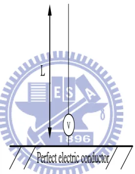
A monopole antenna is one half of a dipole antenna, always mounted above some sort of ground plane. The case of a monopole antenna of length L mounted above an infinite ground plane is shown in Figure 1.
Using image theory, the fields above the ground plane can be found by using the equivalent source (antenna) in free space as shown in Figure 2. This is simply a dipole antenna of twice the length. The fields above the ground plane in Figure 1 are identical to the fields in Figure 2, which are known and presented in the dipole section. The monopole antenna fields below the ground plane in Figure 1 are zero.
Using image theory, the fields above the ground plane can be found by using the equivalent source (antenna) in free space as shown in Figure 2. This is simply a dipole antenna of twice the length. The fields above the ground plane in Figure 1 are identical to the fields in Figure 2, which are known and presented in the dipole section. The monopole antenna fields
Monopole antennas are half the size of their dipole counterparts, and are attractive when a smaller antenna is needed. Antennas on older cell phones were typically monopole antennas, with an infinite ground plane approximated by a small metal plate below the antenna.
Figure 1: The monopole above a PEC
2.1.2 Theory of the Yagi-Uda Structure
Yagi-Uda Antenna is a parasitic linear array of parallel dipoles, see Figure 3, one of which is energized directly by a feed transmission line while the other act as parasitic radiator whose current is induced by mu-tual coupling. The basic antenna is composed of one reflector (in the rear), one driven element, and one or more directors (in the direction of transmis-sion/reception).The Yagi-Uda antenna has received exhaustive analytical and experimental investigations in the open literature and else where. The characteristics of a Yagi are affected by all of the geometric parameters of the array. Usually Yagi-Uda arrays have low input impedance and rela-tively narrow bandwidth.Improvements in both can achieved at the expense of others.
Yagi-Uda consists of a number of metal rods called elements arranged on a central support beam. The elements are a dipole, which is the only driven element arranged with a number of parasitic elements, of which there are a reflector and one or more directors. The function of the parasitic elements is to improve the radiation pattern in the forward direction. The reflector is placed behind the dipole, but having more than one reflector has little benefit. The directors are placed in front and slightly shorter in length than the dipole provide an additional 3dB of forward gain each.
2.2 Design of the Broadband and End-Fired
Milli-meter Wave On-Chip Monopole Antenna for
60GHz
The structure of the proposed broadband and end-fired millimeter wave on-chip cmos antenna is shown in Figure 4 and the layout of the proposed on-chip antenna is shown in Figure 6. The used process of this on-chip antenna is TSMC 0.18 CMOS process. The structure consists of two parts: monopole antenna, and Yagi-Uda antenna. The on-chip antenna size is about 0.7× 0.8mm2.
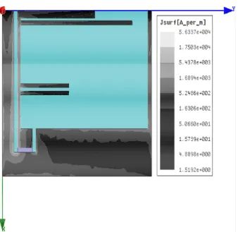
We design the resonant frequency of the antenna to 60GHz by using the theory of monopole antenna. Figure 7 shows the proposed structure of monopole antenna. The distribution of current is shown in Figure 8. Due to it be designed from monopole antenna, the resonant frequency is sensitive from the length of the antenna. So, finding the proposed length of the monopole antenna is the important thing. To reach broadband, we design the extra path to excite another current path. To reach the end-fired radiation pattern, we design it by using properties of Yagi-Uda antenna. There are two stubs which are close to the feeding pad of the antenna. It will work like reflector of Yagi-Uda antenna. On the other hand, we design the antenna structure from Figure 7 to Figure 11. Finally, we complete the antenna that shows in Figure 4.
Figure 4: Configuration of the proposed on-chip antenna
Here, the wavelength is the effective wavelength of the frequency cal-culated by the effective dielectric constant of the substrate [17] and [18].
Figure 6: The layout photo of the on-chip antenna
Figure 7: The structure of the monopole antenna
Figure 9: Add another path to monopole antenna of Figure 7
Figure 10: Before add the another path in the structure of Figure 12
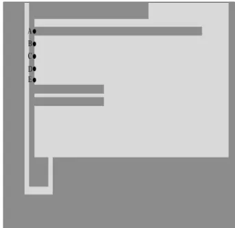
2.3 Simulated Result
First, we definite the point A for feeding point of the on-chip antenna. It is shown in Figure 12. The length of the monopole antenna is important. In this section we will find out the best location for broadband of the antenna. The location is marked from A to E, and it is shown in Figure 13. The different location has different antenna length. The corresponding S-parameter is shown in Figure 14. The result presents what resonant frequency is vary from feeding location. Due to the location also change the center frequency and radiation pattern, we will select the appropriate feeding point. That is point A. To reach broadband, we add the extra path to the proposed antenna, the construction is changed to Figure 12 from figure 10. The corresponding S-parameter is shown in Figure 15. The bandwidth of the proposed antenna will reach 25% from 56GHz to 71GHz.
For the end-fired radiation pattern, we use the Yagi-Uda construc-tion on the monopole antenna. Before using the Yagi-Uda construct, the antenna construct is like Figure 7. The corresponding radiation pattern shown in Figure 16. We can find the difference from front to back about to 1dB. It has not the end-fired performance. So, we add the reflector on the monopole antenna like Figure 12. The corresponding radiation pattern shown in Figure 18. The figure displays the difference from front to back about to 7dB. The simulated result summary is shown in Table 1.
Table 1: The simulated result summary
Simulated results Bandwidth F/B ratio Chip size 60GHz 25% 7dB 0.7× 0.8mm2
Figure 11: The current distribution of the proposed on-chip antenna
Figure 13: The feeding point from A to E
Figure 14: The S-parameter of the corresponding feeding point
Figure 15: The S-parameter of the corresponding construction
Figure 17: Add the reflector in the structure of Figure 7
Figure 18: The radiation pattern of the structure of Figure 11
2.4 Measurement Result
Figure 20 shows the chip micrograph of a fabricated 60 GHz CMOS RFIC on-chip antenna using the TSMC 0.18µm CMOS process. The chip size is 0.7× 0.8mm2. Figure 21 shows the on-wafer measured input VSWR of the antenna which is less than three from 55 to 65 GHz. Compare with the simulation and measurement result, and we show it in Fig.2.16. The simulated antenna radiation efficiency is about 9%. The loss may be due to the CMOS substrate loss.
The absolute power gain of the antenna has been measured on-wafer with the technique presented in [19]. As illustrated in Figure 23, two identical RFIC-on-chip antennas are placed side-by-side separated with a distance R. One antenna is used as a transmitting antenna and the other as a receiving antenna. It is noted that the separated distance R between two identical antennas should be satisfied with the far-field condition [19]. From the Friis power transmission formula, the maximum antenna power gain can be can be rewritten as:
Pr(dBm) = Pt(dBm)+Gt(dB)+Gr(dB)−20log(Rkm−fGHz)−92.4 (1)
where Gt and Gr is the gain of the transmitting and receiving antenna,
Pt is the power transmitted, and Pr is the power received. Since these
two antennas are identical, Gr=Gt=G. The power ratio of the transmitted
and received powers (Pr/Pt) equals to the square of direct transmission
coefficient (S21), which can be directly measured from the VNA. From
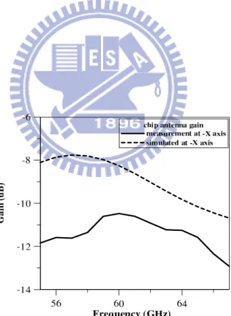
the measured S21 and equation(5), the measured maximum antenna power
gain at 60 GHz is about -10.5 dB, which is slightly less than the simulated result value about -8.8 dB. The figure 18 shows the measurement result of the proposed on-chip antenna about −x axis. The figure 19 shows the comparison gain of the proposed on-chip antenna between measurement and simulated. It has the difference about 1dB. We can regard the phe-nomenon as the loss about the enviroment. The developed CMOS on-chip
transceiver.
Figure 19: The measurement gain of the proposed on-chip antenna
Figure 20: The comparison gain of the proposed on-chip antenna between measurement and simulated
Figure 21: The photograph of the proposed on-chip antenna
Figure 22: The measurement VSWR of the proposed on-chip antenna
Figure 23: The measurement and simulated result of the proposed on-chip antenna
Figure 24: Illustration of the on-wafer measurement setup for the VSWR and power gain of the 60-GHz CMOS RFIC-on-chip monopole antenna
2.5 Conclusion
A 60GHz millimeter-wave on-chip monopole antenna is presented for a 60 GHz WPAN CMOS transceiver application. The CMOS antenna is fabricated with a 0.18µm standard CMOS process. The antenna chip size is 0.7× 0.8mm2. The on-wafer measurement is conducted to measure the input VSWR and the maximum antenna power gain of the on-chip antenna. The simulated antenna radiation efficiency is about 9%, which may be due to the CMOS substrate loss. The simulated antenna pattern performs an end-fire radiation characteristic, and the front-to-back ratio is about 7 dB. The measured input VSWR is less than three from 55 to 65 GHz, and the maximum antenna power gain at 60 GHz is about -10.5 dB. The designed on-chip monopole antenna is useful for the integrated design of the 60GHz CMOS single-chip RF transceiver.
Chapter3
A Novel Method of Beam-Steering Range Greatly for
Leaky-Wave Antenna
The most important property of leaky-wave antenna is beam-scanning while frequency changing. The original MWLA is shown in Figure 24. But it may have some difficulties to design such as matching impedance bandwidth, increasing beam-steering range, decreasing side lobe, minimiz-ing size. Recently there are more and more investigation to increasminimiz-ing beam-steering range. Some paper suggest us to add element for increasing scanning angle [20, 21]. In practical, we should avoid large side lobe level. When side lobe level is large, it will disperse energy from main lobe. If it is too large, it may interrupt signal of the direction in operating frequency. The result induces the gain of main beam to diminish. To deal with the problem, there is a method to provide feedback structure [22]. We also can use remainder power of leaky-wave antenna not only increase scanning range but also decrease side lobe level [23]. It supplies a new structure to reduce side lobe level [24]. In this paper, we proposed a method to reform the leaky-wave antenna. The proposed antenna can reach large frequency scanning region with matching impedance bandwidth and decreasing side lobe level.
3.1 Basic Theory
3.1.1 Theory of the MLKW structure
The microstrip leaky-wave antenna (MLKW) was first constructed by Menzel in 1979, which was based on exciting the first order mode (TE01, leaky mode) of the microstrip line to obtain a radiation characteristics. A simple traveling wave antenna as the microstrip line leaky wave antenna was investigated in [5]. The leaky phenomenon was detected subsequently by Oliner and Lee [6]; the traveling in a microstrip leaky wave antenna would leak power to air due to a small attenuation constant. Comparing to resonator antenna operated in fundamental mode, the microstrip leaky antenna has a larger bandwidth due to the traveling wave in the microstrip line. This leaky mode antenna also posses the advantages of having a low profile, less weight, simple construction, being simple to fabricate and ease of matching. In addition, narrow beam width and frequency scanning characteristics are the extraordinary properties of the microstrip leaky wave antenna’s physical behavior. Recently, this microstrip leaky wave antenna has attracted a lot of interests to investigate.
A major problem of microstrip leaky wave antenna is the length of the structure. The MLWA proposed by Menzel was mentioned in [25] that the length of the antenna requires about five wavelengths to radiate out power efficiently. A short length of the microstrip line would accompany with a large back lobe in radiation pattern. Recent research found that the back lobes could be suppressed by array topology [26] or a taper-loaded antenna end [22]. The array topology in [26] could suppress to 10.5 dB with the length of about 2f0. The back lobes were suppressed 10 dB at 10GHz and
8 dB at 10.5GHz by the radiating circuits in [27] and [28] respectively while the length was 2λ0. However, these designs mentioned above required a
large length (at least 2λ0) or a complicated structure.
3.2 Design of the Novel Method of Beam-Steering
Range Greatly for Leaky-Wave Antenna
The antenna is designed on the two-faced plane. The substrate is made by FR4. This is fabricated on the substrate with a dielectric con-stant of εr=4.4 and loss tangent of δ=0.02. The thickness of substrate is
1.6mm. The bandwidth is 0.55GHz. It is from 4.25GHz to 4.8GHz. To increase frequency scanning region, we add monopole on the proposed an-tenna. The position of monopole that we add is at the open-end of the proposed leaky-wave antenna. Due to the pattern of monopole is broad-side, it can utilize remainder power of the proposed leaky-wave to compose the pattern of conventional leaky-wave antenna. Therefore, the region of frequency scanning becomes wide. The composed pattern not only has prototype of conventional leaky-wave antenna but also has broadside of monopole. Since it utilizes the combination of radiation pattern, the per-formance is better when the monopole property is better. It is well known that the design of the ground plane is important for the monopole. In order to enhance performance of the monopole, therefore, we add vias to connect the ground of the top and bottom. It can increase effect of the ground plane, and can let the top and bottom ground be equivalent volt-age to increase performance of the proposed antenna. The position of the top ground is beside the proposed leaky-wave antenna, and the bottom ground is the shading part in Figure 26. Dimension of ground plane on the top plane is L1× W 1 ,and the ground plane on the bottom plane is
L1× (W 1 + W 2 + W 3 + W 4). Matching impedance bandwidth is
consid-ered for the proposed antenna. It is designed by made a slot on the bottom ground. Two slots are produced on the corpus of the proposed leaky-wave antenna. The dimensions of structure are listed in the Table 2.
Table 2: The dimensions of the proposed antenna W1 57 W10 18 L6 80 W2 1.5 W11 55.5 L7 95 W3 2 W12 5 L8 75 W4 13 W13 6 L9 18 W5 2 L1 100 L10 5 W6 2 L2 3 L1 3 W7 2 L3 15 L12 25 W8 11 L4 11.5 L13 5 W9 6 L5 60 Via radius 0.5 Unit:mm 29
Figure 25: Configuration of the conventional leaky wave antenna
Figure 27: The bottom view of the proposed antenna
3.3 Simulated and Measurement Results
The simulated radiation patterns of the proposed MLWA is shown in Figure 27. The original MLWA pattern of simulation is shown in Figure 28. The simulated results illustrate that the back lobes have been suppressed successfully, and the back lobes of the proposed LKW have been suppressed by about 10 dB at the scanning band from 4.25GHz to 4.8GHz compared to the original MLWA. The measurement radiation pattern of the proposed MLWA is shown in Figure 29. The gain difference between the main beam and back lobe is 10 dB. The back lobes of the proposed MLWA is suppressed indeed in experimental results.
It is noticeable to speak of the scanning angle of the main beams about the proposed MLWA and original MLWA. In simulated radiation pattern, the main beams of the proposed MLWA are slightly slanted to broadside direction compared to the original one. It is mainly due to the monopole of the proposed MLWA. Therefore the scanning region of the proposed MLWA is wider than the original MLWA. In simulated results, the scanning angle of main beam of the proposed MLWA is about 44°, and the original MLWA is about 20°. There is about 24° difference between the proposed MLWA and original MLWA. The measurement scanning region is shown in Figure 29.
Figure 28: The simulated radiation patterns of the proposed MLWA
Figure 29: The simulated radiation patterns of the conventional MLWA
3.4 Conclusion
Here, a novel Method of Beam-Steering Range Greatly for Leaky-Wave Antenna is introduced. We can design the open terminal of original MLKW to improve the performance. The monopole is used in this experiment. This method can effectively improve the performance from comparing the difference between Figure 27 and Figure 28. It not only decreases the back lobes, but increases the scanning region. After we design the proposed MLKW, we have to match the input matching. We design the slot under the feeding line of the proposed MLKW appropriately. Figure 30 shows the comparison about matching and without matching. Finally, we have completed the proposed antenna.
Chapter4
Design Of MIMO Antenna For Application In
2.4GHz
Future wireless communication systems should be capable of accom-modating higher data rates than the current systems owing to the advent of various multimedia services. The use of multielement antennas, such as multiple-input multiple-output (MIMO) antenna systems, is one of the effective ways for improving reliability and increasing the channel capacity. However, it is very difficult to integrate multiple antennas closely in a small and compact mobile handset while maintaining good isolation between an-tenna elements since the anan-tennas couple strongly to each other and to the ground plane by sharing the surface currents on them. For a M×N MIMO communication system, the data throughput can be pushed up to K times, K=min(M,N) that of a single-input single-output (SISO) system, as long as the communication channels linked between the transmitter and the receiver are uncorrelated [29–31]. The correlation between the chan-nels depends not only on the propagation environment, e.g., multipath effect due to the reflection and diffraction of outdoor buildings or indoor partitions, and also on the coupling between the N or M antennas. High antenna coupling (or low isolation) would introduce signal leakage from one antenna to another, thus increasing the signal correlation between the channels. It will also decrease the antenna radiation efficiency due to the loss of the power dissipated in the coupled antenna port. The signal cor-relation between two receiver antennas can be reduced by increasing the antenna spacing. However, this spacing is usually limited, especially for a mobile terminal which has very restricted volume for the antennas. The other way to diminish the correlation is using multiple antennas with dif-ferent radiation patterns. It is better to have the patterns complementary to each other in space, so as to receive multipath signals from various directions.
For a long time, many papers have been focused on diminishing the coupling of antennas. In[32], the relation of the isolation and the
ment of two nearby antennas with different operating bands in a cellular handset were studied. Itoh and the co-workers used the defected ground structure (DGS) to increase the port isolation of polarized and dual-frequency patch antennas[11]. The above tackled the isolation problems of antennas operating at different frequencies. For decoupling two nearby antennas with the same frequency, many efforts have been done by us-ing the electromagnetic band gap (EBG) structures. Mushroom-like EBG structures are the ones that are usually inserted between patch antennas to prevent the propagation of surface waves for higher isolation and better radiation patterns[33–35]. These EBG structures provide conspicuous de-coupling effect, but suffer from complicated structures and large structure area. Possible loss may also be induced in the resonant EBG structures. To reduce the coupling between two planar inverted F antennas (PIFAs), Diallo[12, 36–38] used a suspended metal strip linking the two antennas to cancel the reactive coupling between antennas. This neutralization tech-nique has been also extended to patch antennas by [39] and [40]. In[41], a decoupling circuit network was realized for two-element array by using external transmission lines. Although good isolation was achieved, only weak coupled antennas were tackled. The all-transmission-lines configura-tion also made the circuit bulky. A similar approach of connecting circuits between elements has also been used to improve the impedance matching of a phasedarray antenna over wide scan angles [42] since mutual coupling may vary the input impedance in different scanning angle. The mutual coupling of two closely packed antennas was reduced by etching slots on the ground plane [10]. The fish-bone like slots formed equivalent induc-tors and capaciinduc-tors on the ground plane, which prevented the flowing of the coupling ground current between the antennas. A large ground plane size was needed for sufficient isolation. In this paper, the MIMO antenna will be composed by quadrature hybrid and monopole. We will design the quadrature hybrid in 2.4GHz. It will have the important property of high isolation. On the other hand, it has low relation between signal port. This
system.
4.1Basic Theory of Quadrature Hybrid
Quadrature hybrid are 3dB directional couplers with a 90° phase dif-ference in the outputs of the trough and coupled arms. This type of hybrid is often made in microstrip or stripline form as shown in Figure 31. It is also known as a line hybrid. The basic operation of the branch-line coupler is as follows. With all ports matched, power entering port 1 is evenly divided between ports 2 and 3, with a 90° phase shift between these outputs. No power is coupled to port 4 (the isolated port). We will use this isolated property to apply on the MIMO antenna. The branch-line hybrid has a high degree of symmetry, as any port can be used as the input port. The output ports will always be on the opposite side of the junction from the input port, and the isolated port will be the remaining port on the same side as the input port. The [S] matrix of a reciprocal four-port network matched at all ports has the following form:
S = 0 S12 S13 S14 S12 0 S23 S24 S13 S23 0 S34 S14 S24 S34 0 (2)
If the network is lossless, we can get equation from the unitarity, or energy conservation. Let us consider the multiplication of row 1 and row 2, and the multiplication of row 4 and row 3:
S13∗ S12+ S14∗ S23 = 0 (3a) S14∗ S13+ S24∗ S23 = 0 (3b) Now multiply (7a) by S24∗ and (7b) by S13∗ , and subtract to obtain
S14∗ (|S13|2 − |S24|2) = 0 (4) Similarly, the multiplication of row 1 and row 3, and the multiplication of row 4 and row 2, gives
S12∗ S23+ S14∗ S34 = 0 (5a) S14∗ S12+ S34∗ S23 = 0 (5b)
Now multiply (9a) by S12 and (9b) by S34, and subtract to obtain
S23(|S12|2 − |S34|2) = 0 (6)
One way for (8) and (10) to be satisfied is if S14 = S23 = 0, which results
in a directional coupler. Then the self-products of the rows of the unitary [S] matrix of (6) yield the following equations:
|S12|2 +|S13|2 = 1, (7a) |S12|2
+|S24|2 = 1, (7b)
|S13|2 +|S34|2 = 1, (7c) |S24|2 +|S34|2 = 1 (7d)
which imply that|S13| = |S24|(using (11a) and (11b)), and that|S12| = |S34|(using (11c) and (11d)).
Further simplification can be made by choosing the phase references on three of the four ports. Thus, we choose S12 = S34 = α, S13 = βe(jθ),
and S24 = βe(jϕ), where α and β are real, and θ and ϕ are phase constants
to be determined (one of which we are still free to choose). The dot product of rows 2 and 3 gives
S12∗ S13+ S24∗ S34 = 0, (8)
which yields a relation between the remaining phase constants as
θ + ϕ = π± 2nπ. (9) If we ignore integer multiples of 2π, there are two particular choices that commonly occur in practice:
(1)The Symmetrical Coupler: θ = ϕ = π/2. The phases of the terms having amplitude β are chosen equal. Then the scattering matrix has the following form:
S = 0 S12 S13 S14 S12 0 S23 S24 S13 S23 0 S34 S14 S24 S34 0 (10)
(2) The Antisymmetrical Coupler: θ = 0, ϕ = π. The phases of the terms having amplitude β are chosen to be 180° apart. Then the scattering matrix has the following form:
S = 0 α β 0 α 0 0 −β β 0 0 α 0 −β α 0 (11)
Note that the two couplers differ only in the choice of reference planes. Also, the amplitudes α and β are not independent, as (11a) requires that:
α2 + β2 = 1 (12) We can find the S-parameter matrx from (13) and (14), and four ports are matching, the power supplied to port 1 is coupled to port 3 (the coupled port) with the coupling factor |S13|2 = β2, while the remainder of the
input power is delivered to port 2 (the through port) with the coefficient
|S12|2 = α2 = 1−β2. In an ideal directional coupler, no power is delivered to
ports 4 (the isolated port). Hybrid couplers are special cases of directional couplers, where the coupling factor is 3 dB, which implies that α = β = 1/√2. There are two types of hybrids:
(1)The quadrature hybrid has a 90°phase shift between ports 2 and 3 (θ = ϕ = π/2) when fed at port 1, and is an example of a symmetrical coupler. Its [S] matrix has the following form
S = 0 1 j 0 1 0 0 j j 0 0 1 0 j 1 0 (13)
(2)The magic-T hybrid or rat-race hybrid has a 180°phase difference be-tween ports 2 and 3 when fed at port 4, and is an example of an antisymmetrical coupler. Its [S] matrix has the following form:
S = √1 2 0 1 j 0 1 0 0 j j 0 0 1 0 j 1 0 (14) 43
4.2Design of the MIMO Antenna
For high isolation MIMO antenna, we select the isolated port of quadra-ture hybrid to design. Figure 32 shows the port name. To wireless com-munication device, we have to design the antenna radiation pattern to the omni-direction. So, monopole is used in the MIMO antenna. The other reason that we use monopole antenna is the omni-directional radiation pattern. The qudrature hybrid frequency is 2.4GHz. Figure 33 shown the coupler construction in 2.4GHz. The S-parameter of coupler is shown in Figure 34. Then, we add monopole on the coupler like Figure 35. This construction is called original MIMO antenna in the research. There is a problem in the original antenna, that is phase. The phase difference be-tween P3 and P4 is about 90°. P3 and P4 are fed from P1 simultaneously. It will lead to the power not the same about each monopole antenna. This have not good performance about MIMO antenna. To solve this problem, we design path on the coupler to assure that the power is the same on each monopole antenna. The coupler is shown in Figure 36 after the phase is solved. Then we select the approach monopole antenna to add on the cou-pler. Figure 37 shown the construction. To enhance the isolation, the strip resonator on the ground between two monopole antenna is designed. The method can decrease the relation between two antenna, and increase the isolation. Finally, we consider the matching about MIMO antenna that is composed by coupler and antenna. The complete MIMO antenna is shown in Figure 39.
Figure 33: The structure of quadrature hybrid coupler with port name
Figure 35: The S-parameter of the quadrature hybrid coupler
Figure 36: Add monopole to the quadrature hybrid coupler
Figure 37: Configuration that is without phase difference
Figure 39: The structure is to decouple the MIMO antenna
Figure 40: The structure is to match the S-parameter
4.3Simulated and Measurement Result
The antenna was designed and simulated using Ansoft’s HFSS full-wave simulator. Figure 40 shows the relation about the MIMO antenna construction of Figure 35. Because the phase of power to two antennas is out of phase, it does not have good performance of MIMO performance. In this research, good performance is like high isolation between two an-tennas and omni-directional radiation pattern. So, we modify the path from Figure 35 to Figure 37. It will have the same degree of phase to feed two antennas. To reach inphase of the power, we construct the coupler to Figure 36. For port1 to port3 and port1 to port4, we can find that the difference of degree is 0°. Figure 42 shows the difference of degree. In other words, they are inphase. Then, for port2 to port3 and port2 to port4, we can find that the difference of degree is about 180°. Figure 43 shows the difference of degree. Because the period of electromagnetic wave length is 180°, it is inphase too. The Figure 38 is the method of being inphase about two antennas. It has the relation about two antenna in Figure 41. It can decrease the relation about 2dB from the value of the difference of Figure 40 and Figure 41 in 2.4GHz. This construction can also improve the performance of the radiation pattern. Figure 44 shows the radiation pat-tern of the construction of Figure 37. The radiation patpat-tern become more omni-directional after the construction is modified. Figure 45 shows the radiation pattern. We can compare the radiation pattern between Figure 44 and Figure 45. The construction of Figure 37 can improve the radiation pattern to omni-direction. So, we can demonstrate that the method can improve the performance for MIMO antenna. To enhance the isolation, we add the strip resonator on the ground between two antennas. The con-struction is like as Figure 38. The isolation is shown in Figure 46 after we add the strip resonator. We can find that the isolation is decreasing about 3dB after the rod is added. The isolation is about -25dB in the Fig-ure 46. It is effective to decrease the relation by adding the rod between
research, the open stubs is used to match the input impedance. Figure 47 shows the input impedance before we use open stubs. It does not match in the bandwidth that we design. So, we design the construction to solve the problem. The construction is like as Figure 39. The input impedance is shown in Figure 48 after open stubs is designed. The input impedance is matched in the bandwidth that we design. It can reach less than -10dB in the bandwidth that we want. Figure 39 is the final construction of MIMO antenna. Figure 49 is the simulated S-parameter of the research for com-plete MIMO antenna. Figure 50 is the measurement S-parameter of the research for complete MIMO antenna. The simulated result is agreement with the measurement result about S-parameter. The measurement radia-tion pattern of the proposed MIMO antenna is shown in Figure 51. Figure 51 and Figure 52 displays the radiation pattern of the simulated and mea-surement result. The environment of meamea-surement result of Figure 51 is the proposed MIMO antenna to be fed in port 1, and to be terminated in port 2. Then the environment of measurement result of Figure 52 is the proposed MIMO antenna to be fed in port 2, and to be terminated in port 1.
Figure 41: The simulated S-parameter of the contribution of Figure 33
Figure 43: The difference of degree from port1 to port3 and port1 to port4 respectivly
Figure 44: The difference of degree from port2 to port3 and port2 to port4 respectivly
Figure 45: The radiation pattern for the structure of Figure35
Figure 47: The simulated relationship between two ports of Figure 36
Figure 48: The S-parameter before we add open stubs to match
Figure 49: The S-parameter after we add open stubs to match
Figure 51: The measurement S-parameter for the proposed MIMO antenna
Figure 52: The radiation pattern about simulated and measurement result
4.4Conclusion
Here, we have presented the MIMO antenna. This structure is com-posed by quadrature hybrid and monopole antenna. The quadrature hybrid can offer high isolation by its property. For handset device, we have to have omni-directional radiation pattern. So, the monopole antenna is selected. Quadrature hybrid and monopole antenna can provide good performance that we want in wireless communication. To enhance the isolation, we add the strip resonator between two antennas. It can guide the energy of antenna coupling each other to the ground. Hence, we have high isolation MIMO antenna.
We know what high isolation is equal to high S/N. From Shannon equation, high S/N can increase the channel capacity. So, the higher iso-lation the better performance for MIMO antenna.
Chapter5
Conclusion And Future Study
5.1Conclusion and Summary
Here, we will summarize the conclusions of three topics. The first topic, on-chip antenna, has been integrated in the MMIC or the RFIC. It can provide specifications that we want. Like as radiaion pattern and return loss. For radiation pattern, high F/B ratio is what we want to have. Due to the proposed on-chip antenna be designed to avoid the radiation pattern interfering with the back circuit, high F/B ratio is more important obviously. So we select the construction of Yagi-Uda to implement the effect.
Then, the second topic, a novel structure antenna for leaky-wave an-tenna, we have reached performance of the wide frequency sacnning range and the decreasing side lobe level. The proposed antenna of monopole at the open end of the leaky wave antenna is the mainly design.
For the third topic, high isolation MIMO antenna, we have provided the antenna of performance of high isolation about two antennas and the omni-directional radiation pattern. The isolation can reach about -25dB. It can increase the channel capacity and S/N ratio when the isolation of two antennas is high. It can also cancel the effect of antenna array to reach omni-directional radiation pattern for personal communication device in-directly. The other antenna characteristic is omni-directional radiation pattern. Because we have the proposed antenna to apply to personal com-munication device, the omni-directional radiation pattern is designed.
5.2Future Study
In the future, there still have some topics we can reasearch. For the on-chip antenna, the size decreasing, high radiation effeciency, and radiation pattern that we require. For the second topic, leaky wave antenna, side lobe level decreasing, frequency scanning region increasing, total size decreasing, and operating frequency increasing. It will have many ways to design the open end of the leaky wave antenna to enhance the performance. In our research, the monopole is added to enhance the frequency scanning range. We can use many ways to design the leaky wave antenna to reach not only increasing frequency scanning range but decreasing the size of the proposed antenna.
For MIMO antenna, increasing isolation between antennas is the most important. The number of antenna is more than 2. So, decreasing the relationship between antennas is more difficult. In MIMO antenna, the decoupling device is the important component. There are many ways to design the decoulping device, and good designing not only decouple an-tennas but match the impedance of every antenna. Decreasing the size of the decoupling device is another research. In the future, we can utilize the decoupling devive to combinate radiated antennas to reach the perfor-mance what we want. For instance, we want to generate circle polarization MIMO antenna. we will design the circle polarization antennas and de-coupling device to improve the antenna performance. It will be worthy to research the combination of decoupling device and radiated antennas.
Reference
[1] P. Smulders. “exploring the 60 ghz band for local wireless multime-dia access: Prospects and future directions,”. IEEE Commun, vol. 40(No.1):140–147, Jan 2002.
[2] C.H. Doan, S. Emami, A.M. Niknejad, and R.W. Brodersen. “design of cmos for 60ghz applications,”. In Solid-State Circuits Conference,
2004. Digest of Technical Papers. ISSCC. 2004 IEEE International,
pages 440–538. IEEE, 2004.
[3] Y.P. Zhang, M. Sun, and LH Guo. “on-chip antennas for 60-ghz ra-dios in silicon technology,”. Electron Devices, IEEE Transactions on, 52(7):1664–1668, 2005.
[4] S.S. Hsu, K.C. Wei, C.Y. Hsu, and H. Ru-Chuang. “a 60-ghz millimeter-wave cpw-fed yagi antenna fabricated by using 0.18µ cmos technology,”. Electron Device Letters, IEEE, 29(6):625–627, 2008. [5] W. Menzel. “a new travelling wave antenna in microstrip,”. In
Mi-crowave Conference, 1978. 8th European, pages 302–306. IEEE, 1979.
[6] A.A. Oliner and KS Lee. “the nature of the leakage from higher modes on microstrip line,”. In Microwave Symposium Digest, 1986 IEEE
MTT-S International, pages 57–60. IEEE, 1986.
[7] C.Y. Chiu, J.B. Yan, and R.D. Murch. “compact three-port orthogo-nally polarized mimo antennas,”. Antennas and Wireless Propagation
Letters, IEEE, 6:619–622, 2007.
[8] C.Y. Chiu, J.B. Yan, and R.D. Murch. “24-port and 36-port antenna cubes suitable for mimo wireless communications,”. Antennas and
Propagation, IEEE Transactions on, 56(4):1170–1176, 2008.
[9] S.C. Chen, Y.S. Wang, and S.J. Chung. “a decoupling technique for increasing the port isolation between two strongly coupled antennas,”.
[10] C.Y. Chiu, C.H. Cheng, R.D. Murch, and C.R. Rowell. “reduction of mutual coupling between closely-packed antenna elements,”. Antennas
and Propagation, IEEE Transactions on, 55(6):1732–1738, 2007.
[11] Y. Chung, S.S. Jeon, D. Ahn, J.I. Choi, and T. Itoh. “high isolation dual-polarized patch antenna using integrated defected ground struc-ture,”. Microwave and Wireless Components Letters, IEEE, 14(1):4–6, 2004.
[12] A. Diallo, C. Luxey, P. Le Thuc, R. Staraj, and G. Kossiavas. “en-hanced two-antenna structures for universal mobile telecommunica-tions system diversity terminals,”. Microwaves, Antennas and
Propa-gation, IET, 2(1):93–101, 2008.
[13] L. Inclan-Sanchez, J.L. Vazquez-Roy, and E. Rajo-Iglesias. “high iso-lation proximity coupled multilayer patch antenna for dual-frequency operation,”. Antennas and Propagation, IEEE Transactions on,
56(4):1180–1183, 2008.
[14] A.C.K. Mak, C.R. Rowell, and R.D. Murch. “isolation enhancement between two closely packed antennas,”. Antennas and Propagation,
IEEE Transactions on, 56(11):3411–3419, 2008.
[15] J. Guterman, A.A. Moreira, and C. Peixeiro. “integration of omnidi-rectional wrapped microstrip antennas into laptops,”. Antennas and
Wireless Propagation Letters, IEEE, 5(1):141–144, 2006.
[16] C.Y. Chiu and R.D. Murch. “compact four-port antenna suitable for portable mimo devices,”. Antennas and Wireless Propagation Letters,
IEEE, 7:142–144, 2008.
[17] H.R. Chuang and L.C. Kuo. “3-d fdtd design analysis of a 2.4-ghz polarization-diversity printed dipole antenna with integrated balun and polarization-switching circuit for wlan and wireless communica-tion applicacommunica-tions,”. Microwave Theory and Techniques, IEEE
Trans-actions on, 51(2):374–381, 2003.
[18] LC Kuo, H.R. Chuang, YC Kan, TC Huang, and CH Ko. “a study of planar printed dipole antennas for wireless communication applications,”. Journal of Electromagnetic Waves and Applications, 21(5):637–652, 2007.
[19] RN Simions and RQ Lee. “on-wafer characterization of millimeterwave antennas for wireless application,”. IEEE Trans. Microw. Theory Tech, 47(1):92–96, 1999.
[20] G. Augustin, SV Shynu, P. Mohanan, CK Aanandan, and K. Vasude-van. “a novel leaky wave antenna capable for electronic beam steer-ing,”. In Antennas and Propagation Society International Symposium
2006, IEEE, pages 4255–4258. IEEE.
[21] Y. Li, Q. Xue, E.K.N. Yung, and Y. Long. “quasi microstrip leaky-wave antenna with a two-dimensional beam-scanning capability,”.
An-tennas and Propagation, IEEE Transactions on, 57(2):347–354, 2009.
[22] Y.C. Shih, S.K. Chen, C.C. Hu, and CF Jou. “active feedback mi-crostrip leaky wave antenna-synthesiser design with suppressed back lobe radiation,”. Electronics Letters, 35(7):513–514, 1999.
[23] Y.L. Chiou, J.W. Wu, J.H. Huang, and C.F. Jou. “design of short mi-crostrip leaky-wave antenna with suppressed back lobe and increased frequency scanning region,”. Antennas and Propagation, IEEE
Trans-actions on, 57(10):3329–3333, 2009.
[24] J.W. Wu, C.J. Wang, and C.F. Jou. “method of suppressing the side lobe of a tapered short leaky wave antenna,”. Antennas and Wireless
Propagation Letters, IEEE, 8:1146–1149, 2009.
[25] A. Oliner and K. Lee. “microstrip leaky wave strip antennas,”. In
An-tennas and Propagation Society International Symposium, 1986,
vol-ume 24, pages 443–446. IEEE, 1986.
[26] C.J. Wang, C.F. Jou, J.J. Wu, and S.T. Peng. “radiation characteris-tics of active frequency-scanning leaky-mode antenna arrays,”. IEICE
transactions on electronics, 82(7):1223–1228, 1999.
[27] C.J. Wang, H.L. Guan, and C.F. Jou. “a novel method for short leaky-wave antennas to suppress the reflected wave,”. Microwave and
Optical Technology Letters, 36(2):129–131, 2003.
[28] I.Y. Chen, C.J. Wang, H.L. Guan, and C.F. Jou. “studies of sup-pression of the reflected wave and beam-scanning features of the an-tenna arrays,”. Anan-tennas and Propagation, IEEE Transactions on, 53(7):2220–2225, 2005.
[29] A.J. Paulraj, D.A. Gore, R.U. Nabar, and H. Bolcskei. “an overview of mimo communications-a key to gigabit wireless,”. Proceedings of
the IEEE, 92(2):198–218, 2004.
[31] T. Hult and A. Mohammed. “compact mimo antennas and hap diver-sity for enhanced data rate communications,”. In Vehicular
Technol-ogy Conference, 2007. VTC2007-Spring. IEEE 65th, pages 1385–1389.
IEEE.
[32] Z. Li and ” Rahmat-Samii, Y. “optimization of pifa-ifa combination in handset antenna designs. Antennas and Propagation, IEEE
Trans-actions on, 53(5):1770–1778, 2005.
[33] F. Yang and Y. Rahmat-Samii. “microstrip antennas integrated with electromagnetic band-gap (ebg) structures: A low mutual coupling de-sign for array applications,”. Antennas and Propagation, IEEE
Trans-actions on, 51(10):2936–2946, 2003.
[34] Z. Iluz, R. Shavit, and R. Bauer. “microstrip antenna phased array with electromagnetic bandgap substrate,”. Antennas and Propagation,
IEEE Transactions on, 52(6):1446–1453, 2004.
[35] L. Yang, M. Fan, F. Chen, J. She, and Z. Feng. “a novel compact electromagnetic-bandgap (ebg) structure and its applications for mi-crowave circuits,”. Mimi-crowave Theory and Techniques, IEEE
Trans-actions on, 53(1):183–190, 2005.
[36] A. Diallo, C. Luxey, P. Le Thuc, R. Staraj, and G. Kossiavas. “study and reduction of the mutual coupling between two mobile phone pifas operating in the dcs1800 and umts bands,”. Antennas and
Propaga-tion, IEEE Transactions on, 54(11):3063–3074, 2006.
[37] A. Diallo, C. Luxey, P. Le Thuc, R. Staraj, G. Kossiavas, M. Franzen, and P.S. Kildal. “mimo performance of enhanced umts four-antenna structures for mobile phones in the presence of the users head,”. In
An-tennas and Propagation Society International Symposium, 2007 IEEE,
pages 2853–2856. IEEE, 2007.
[38] A. Diallo and C. Luxey. “estimation of the diversity performance of several two-antenna systems in different propagation environments,”. In Antennas and Propagation Society International Symposium, 2007
IEEE, pages 2642–2645. IEEE.
[39] S. Ranvier, C. Luxey, P. Suvikunnas, R. Staraj, and P. Vainikainen. “capacity enhancement by increasing both mutual coupling and ef-ficiency: A novel approach,”. In Antennas and Propagation Society
International Symposium, 2007 IEEE, pages 3632–3635. IEEE, 2007.
[40] T.W. Kang and K.L. Wong. “isolation improvement of 2.4/5.2/5.8 ghz wlan internal laptop computer antennas using dual-band strip res-onator as a wavetrap,”. Microwave and Optical Technology Letters, 52(1):58–64, 2010.
[41] J. Andersen and H. Rasmussen. “decoupling and descattering networks for antennas,”. Antennas and Propagation, IEEE Transactions on, 24(6):841–846, 1976.
[42] P. Hannan, D. Lerner, and G. Knittel. “impedance matching a phased-array antenna over wide scan angles by connecting circuits,”. Antennas