國 立 交 通 大 學
電子工程學系 電子研究所碩士班
碩 士 論 文
隨機電報訊號量測法應用於前瞻CMOS元件應變技
術引致的汲極電流不穩定性之研究
The Observation of Strain Induced Drain Current
Instability in Advanced CMOS Devices
Using Random Telegraph Noise Analysis
研 究 生 :林米華
指導教授 :莊紹勳 博士
隨機電報訊號量測法應用於前瞻CMOS元件應變
技術引致的汲極電流不穩定性之研究
The Observation of Strain Induced Drain Current
Instability in Advanced CMOS Devices
Using Random Telegraph Noise Analysis
研 究 生 : 林米華 Student : Mi-Hua Lin
指導教授 : 莊紹勳 博士 Advisor : Dr. Steve S. Chung
國立交通大學
電子工程學系 電子研究所碩士班
碩士論文
A Thesis
Submitted to Department of Electronics Engineering & Institute
of Electronics College of Electrical Engineering and Computer
Science
National Chiao Tung University
in Partial Fulfillment of the Requirements
for the Degree of Master of Science
in Electronics Engineering
August 2009
Hsinchu, Taiwan, Republic of China.
隨機電報訊號量測法應用於前瞻CMOS元件應變
技術引致的汲極電流不穩定性之研究
學生:林米華 指導教授:莊紹勳博士
國立交通大學電子工程學系電子研究所碩士班
摘要
近年的可靠度研究中,施加應變會對CMOS元件造成的熱載子退
化。對於n型MOSFET元件,介電層覆蓋式(CESL)元件(為單軸應變)
有較佳的可靠度、性能表現和簡易的製程。而SiC在S/D 的結構提供
了高的驅動電流。在p型MOSFET 元件中,單軸的應變結構SiGe在S/D
及嵌入式擴散阻擋層(EDB),有著良好的可靠度和效能。
本論文中,我們利用汲極電流隨機電報訊號量測法,觀察在前瞻
應變矽元件,不同的應變技術所造成的缺陷以及可靠度的分析。首
先,在應變n型及p型MOSFET元件中,經熱載子加壓後,造成的電流
衰退,並在汲極端產生缺陷,此缺陷捕捉及釋放通道的載子,造成汲
極電流的不穩定性。藉由載子的捕捉和釋放時間進行統計分析,可以
獲得缺陷的特性。此外,透過單軸應變n型及p型MOSFETs 元件,我
們探討了不同方向的應變技術所引致的汲極電流不穩定性。
amplitude)進而觀察垂直應變和水平應變技術對於熱載子破壞所造成
的退化影響。相較於對於SiGe S/D結構,介電層覆蓋式(CESL)元件
中,此覆蓋層會在閘極介電層中額外的垂直應變結構,經熱載子破壞
後會引致額外的載子散射現象;而SiGe只提供在S/D方向的壓縮應
變,對於可靠度沒有額外的影響。最後,我們亦將此方法應用在SiC
S/D結構元件上,因SiC亦只提供S/D方向的張力應變,無額外的應變
在介電層中,此實驗結果可加以驗證之前的結果,與SiGe S/D結構類
似,亦即其通道的應變效應,對於可靠度沒有額外的影響。
The Observation of Strain Induced Drain Current
Instability in Advanced CMOS Devices
Using Random Telegraph Noise Analysis
Student:Mi-Hua Lin Advisor:Dr. Steve S. Chun
g
Department of Electronics Engineering & Institute of Electronics
National Chiao Tung University
ABSTRACT
Recent study on the reliability issues, the strained devices show a higher impact ionization rate, i.e., the device degradation is proportional to the current enhancement. For n-MOSFET devices, CESL (contact etching stop layer) strain (uniaxial) is much better in terms of reliability, performance, and process simplicity; SiC on source and drain structure shows high driving current ability. For p-MOSFET device, uniaxial structure with SiGe on source and drain with EDB (embedded diffusion barrier) seems to be promising in terms of its performance and reliability.
In this thesis, the hot-carrier stress induced oxide traps and its correlation with enhanced degradation in strained CMOS devices have been reported. First, the ID-RTN (Drain Current Random Telegraph Noise) has been employed to study the
stress induced slow traps in uniaxial strained n-MOSFETs and p-MOSFETs. The carrier trapping and detrapping effect in the gate dielectric can be observed. The drain current fluctuation is at low level when carrier is trapped and is at high level when
emission time, we can figure out the trap properties. Secondly, different process-induced strain effect for n-MOSFETs and p-MOSFETs has been observed respectively. By extracting the normalized drain current amplitude from the drain current spectra, experimental results show that the vertical compressive strain generates extra oxide defects and induces more scattering after HC stress in CESL device.
This vertical strain in CESL also contributes to a non-negligible amount of extra devices degradation. While, SiGe S/D on p-MOSFET device shows different behavior in that the compressive strain along the channel shows no impact on its reliability. The process induced strain among different strained techniques can be investigated by the ID-RTN measurement. Furthermore, the application to the study of the strained SiC on
S/D has also been demonstrated. Results also show that the uniaxial strain in such device exhibits less impact on the device reliability. Therefore, this strained SiC device is similar to the SiGe S/D device in terms of the ID-RTN characteristics.
Acknowledgements
碩士生活的兩年是短暫卻又充實的,交織著酸甜苦辣的實驗室日子。首先要 感謝我的指導教授莊紹勳老師,莊老師不僅在研究上給予許多指導建議,教我應 具有的研究精神跟態度,並在課業與生活上,也有許多的關懷,在此深表我對老 師的感謝。 感謝家銘學長在實驗研究上的細心教導,並且給予我許多的建議跟指導,感 謝建鴻、友良、易叡和文彥學長,給予學業跟實驗上的解答跟協助。還有感謝這 兩年研究生涯的夥伴安舜、健宏、振鵬,在日常的生活中,因為有你們,讓實驗 研究生活變得更加有趣,相信數年後再聚,定倍感溫馨。也感謝汪老師研究群的 志昌、達達、小馬、佑亮、元元學長,彥君、子華學姐、以及阿標和阿杜,雖然 在不同的研究群中,但實驗室有你們,使得乏味的實驗室生活更多采多姿。此外, 也感謝學弟元宏、政穎、永涵、士嵩,感謝你們對實驗室的付出,使得學長姐們 能專心於實驗研究上,真心的祝福你們明年可以順利畢業。總歸一句,感謝所有 的夥伴,因為有你們,使我這兩年研究生活豐富且精彩,即使艱辛,仍充滿歡笑。 另外,在此也要感謝聯華電子在測試元件和儀器上的協助,讓本研究才得以 順利完成。 最後要感謝我家人們,你們是我最大的精神支柱,有了你們的支持和鼓勵, 讓我能堅持到現在。 謹將這份榮耀獻給培育我多年的父母親。Contents
Chinese Abstract --- i
English Abstract --- iii
Acknowledgements --- v
Content --- vi
Figure Captions --- ix
Chapter 1 Introduction……….……….… 1
1.1 The Motivation of this Work………
…..
………….
11.2 Organization of the Thesis……….. 2
Chapter 2 Random Telegraph Noise Mechanism and Experimental Setup……...….. 3
2.1 Introduction……….………... 3
2.2 Experimental Setup………..……….………. 3
2.3 Theory of Drain Current Telegraph Noise…………..………... 5
Chapter 3 Random Telegraph Noise of Drain current in n-MOSFETs……… 10
3.1 Introduction……….…... 10
3.2 Device Preparation……….……… 11
3.3 The Analysis of Reliability in n-MOSFETs………... 11
3.3.1 Introduction………...………...…………... 11
3.3.2 Drain Current Degradation………...……... 12
3.4 The Analysis of ID-RTN in n-MOSFETs……….…….……….. 13
3.4.1 Drain Current Waveform………...………. 13
3.4.2 Capture and Emission time…..………...……… 13
3.5 Discussion………... 14
3.5.1 Trap Depth……….………. 15
Chapter 4 Random Telegraph Noise of Drain Current in p-MOSFETs………...
30
4.1 Introduction……… 30
4.2 Device Preparation………. 31
4.3 The Analysis of Reliability in p-MOSFETs………... 31
4.3.1 Introduction…………...……….…..………... 31
4.3.2 Drain Current Degradation……… 32
4.4 The Analysis of ID-RTN in p-MOSFETs……….………... 33
4.4.1 Drain Current Waveform………...……….……… 33
4.4.2 Capture and Emission time…..…...………...………. 33
4.5 Discussion………... 33
4.5.1 Trap Depth……….. 33
4.5.2 Normalized Drain Current Amplitude………...………. 34
4.6 Comparison Between n- and p-MOSFETs………..………...……… 34
4.6.1 Introduction…...………...………... 34
4.6.2 Normalized Drain Current Amplitude………...………. 35
4.6.2.1 Experimental Result……… 35
4.6.3 ID-RTN: Normalized Drain Current Amplitude………...…….. 35
4.6.4 Discussion………...…... 36
Chapter 5 Application to Strained SiC Devices ………...
515.1 Introduction……….... 51
5.2 Device Preparation………. 51
5.3 The Analysis of Reliability in SiC Devices….………... 52
5.3.1 Introduction……… 52
5.3.2 Drain Current Degradation………. 52
5.4 The Analysis of ID-RTN in SiC Devices….………... 53
5.5 Discussion……….……… 53
5.5.1 Trap Depth……….……… 53
5.5.2 Normalized Drain Current Amplitude………... 54
Chapter 6 Summary and Conclusion………...… 67
Figure Captions
Chapter 2
Fig. 2.1 The measurement setup using Analyzer HP 4156C to sampling as RTN processing. Notably
there is not switch equipment HP 5250 here.
Fig. 2.2 The terminals setup for sampling by Analyzer HP4156C.
Fig. 2.3 (a) Carrier trapping and detrapping by the slow trap near the drain side. (b) Illustration of
the three parameter of the RTN noise: capture time c, emission time e, and current fluctuation with amplitudeΔID.
Chapter 3
Fig. 3.1 The cross-section view of the experimental devices. (a) bulk-Si and (b) CESL (contact
etching stopping layer) devices (uniaxial-strained). Both of them are <100> channel on (100) substrate.
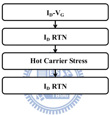
Fig. 3.2 The operating procedure of the following analysis for the devices.
Fig. 3.3 The comparison of ID-VD characteristic in n-MOSFET devices before and after the HC stress, (a) bulk-Si and (b) CESL devices.
Fig. 3.4 Drain current waveform of bulk-Si deviceat T= 25℃.
Fig. 3.5 Drain current waveform of CESL device at T= 25℃.
Fig. 3.6 Variation of capture time c, (filled symbol) and emission time e (open symbol) as gate voltage increases for bulk-Si device.
Fig. 3.7 Variation of capture time c, (filled symbol) and emission time e (open symbol) as gate voltage increases for CESL device.
Fig. 3.10 The effective depth location for the two traps in, (a) bulk-Si and (b) CESL devices.
Fig. 3.11 Normalized RTN amplitude (filled symbol) and normalized conductance change (open
symbol) versus gate voltage for bulk-Si device.
Fig. 3.12 Normalized RTN amplitude (filled symbol) and normalized conductance change (open
symbol) versus gate voltage for CESL device.
Chapter 4
Fig. 4.1 The cross-section view of the experimental devices, (a) bulk-Si, and (b) SiGe on S/D
device (biaxial-strained). Both of them are <110> channel on (100) substrate.
Fig. 4.2 The comparison of ID-VD characteristic in p-MOSFET devices before and after the HC stress, (a) bulk-Si and (b)SiGe S/D devices.
Fig. 4.3 Drain current waveform of bulk-Si device at T= 25℃. Fig. 4.4 Drain current waveform of SiGe S/D device at T= 25℃.
Fig. 4.5 Variation of capture time c (filled symbol) and emission time e (open symbol) as gate voltage increases for bulk-Si device.
Fig. 4.6 Variation of capture time c (filled symbol) and emission time e (open symbol) as gate voltage increases for SiGe on S/D device.
Fig. 4.7 Capture time over emission time versus gate voltage plots for p-MOSFETs.
Fig. 4.8 The effective depth location for the two traps in, (a) bulk-Si and (b) SiGe on S/D devices. Fig. 4.9 Normalized RTN amplitude (filled symbol) and normalized conductance change (open
symbol) versus gate voltage for bulk-Si device.
Fig. 4.10 Normalized RTN amplitude (filled symbol) and normalized conductance change (open
symbol) versus gate voltage for SiGe on S/D device.
Fig. 4.11 Illustration of the various strains for (a) CESL and (b) SiGe on S/D devices. Fig. 4.12 The comparison of CP current for bulk-Si and CESL devices.
Fig. 4.14 Normalized current amplitude versus overdrive voltage. (left) n-MOSFET (right)
p-MOSFET. Note that the huge drop for CESL is caused by the vertical strain in CESL n-MOSFET.
Chapter 5
Fig. 5.1 The cross-section view of the experimental devices, (a) bulk-Si and (b) SiC on S/D devices
(uniaxial-strained). Both of them are <100> channel on (100) substrate. The terminals setup using Analyzer HP 4156C to sampling.
Fig. 5.2 The comparisons of ID-VD characteristics in n-MOSFET devices before and after the HC stress, (a) bulk-Si and (b) SiC on S/D devices.
Fig. 5.3 Drain current waveform of bulk-Si device at T= 25℃. Fig. 5.4 Drain current waveform of SiC on S/D device at T= 25℃.
Fig. 5.5 Variation of capture time c (filled symbol) and emission time e (open symbol) as gate voltage increases for bulk-Si device.
Fig. 5.6 Variation of capture time c (filled symbol) and emission time e (open symbol) as gate voltage increases for SiC on S/D device.
Fig. 5.7 Capture time over emission time versus gate voltage plots for n-MOSFETs.
Fig. 5.8 The effective depth location for the two traps in, (a) bulk-Si and (b)SiC on S/D devices. Fig. 5.9 Normalized RTN amplitude (square symbol) and normalized conductance change (circle
symbol) versus gate voltage for bulk-Si device.
Fig. 5.10 Normalized RTN amplitude (square symbol) and normalized conductance change (circle
symbol) versus gate voltage for SiC on S/D device.
Fig. 5.11 Normalized current amplitude versus overdrive voltage for bulk-Si and SiC on S/D devices. Fig. 5.12 Illustration of the strain direction for SiC on S/D device.
Chapter 1
Introduction
1.1 The Motivation of this Work
Recent developments [1.1] in CMOS technology have highlighted the need in using the strain technique as a method to extend the scaling of CMOS device for high speed and low power logic applications. Several approaches among them, such as process-induced stress techniques, strained SiGe channel devices, substrate engineering, and hybrid substrate technology, have been utilized to improve device performance. Although the strained devices enhance the carrier mobility, their reliabilities become a serious issue as reported in [1.2] [1.3].
In the small area devices, carriers are trapped and detrapped stochastically by the traps in the gate dielectric would induce the drain current instability called ID-RTN (Drain Current Random Telegraph Noise). The performance of ultra-scaled devices is highly affected by the local phenomenon.
The ID-RTN method is believed to be one of the great techniques to study the generated oxide traps via carrier trapping and detrapping. So far, the trap-related reliability issues in strained CMOS devices have not been well understood yet.
For the first time, in this thesis, we apply the ID-RTN method to the observation of oxide traps in various n-MOSFETs and p-MOSFETs employing different process-induced strain. The impact of their strains on the device reliability will be investigated and
compared. Furthermore, the application to the SiC on S/D devices will be demonstrated.
1.2 Organization of the Thesis
The thesis is divided into six chapters. Chapter 1 is the introduction. Chapter 2 describes the experiment setups and the ID-RTN mechanism. In chapters 3 and 4, we will first utilize the ID-RTN method to observe the process-induced RTN behavior of strained n-MOSFETs and p-MOSFETs respectively. The hot carrier stress would be applied on the strained CMOS devices. Then, we will discuss the strain induced degradation for n-MOSFETs and p-MOSFETs with different strained techniques. In chapter 5, the application to the SiC S/D device will be studied. Finally, a summary and conclusion will be included in Chapter 6.
Chapter 2
Random Telegraph Noise Mechanism
and Experimental Setup
2.1 Introduction
Recent developments in strained technology have heightened the need for the high performance CMOS devices. The charge pumping measurement can be used to measure the fast trap properties [2.1]. However, the charge pumping current becomes very small in the small area devices that would influence the experimental results for reliability. In order to discriminate the relationship between performance and reliability properties of the small size strained CMOS devices, we utilize the Drain Current Random Telegraph Noise (ID-RTN) measurement technique in this work. In this chapter, the measurement setup and the physics of the drain instability will be described.
This chapter is divided into two sections. First, we will illustrate the fundamental experimental setup to characterizing strained CMOS devices. Second, the ID-RTN technique used in this thesis will be introduced, and its fundamental theory will be described.
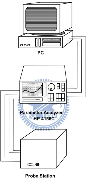
2.2 Experimental Setup
The experimental setup for the direct current I–V and the ID-RTN measurement of semiconductor devices is illustrated in Fig. 2.1 and Fig. 2.2, respectively. Through the PC controlled instrument environment, the complicated and long-term characterization
procedure for analyzing the intrinsic and degradation in MOSFETs can be easily verified. As shown in Fig. 2.1, the characterization equipment, including semiconductor parameter analyzer (HP4156C), and cascade guarded thermal probe station, provides an adequate capability for measuring the device characteristics. In this method, the pulse generator is not included that would decreases the influence from the noise. In addition, the PC program used to control all the measurement process is HT-basic. The parameter analyzer is connected to the probe station directly without passing through the switch equipment. At the room temperature, the sampling mode is chosen and the VGS, VDS bias is selected to make the trap’s energy level in the vicinity of the Fermi level. For the sampling rate, the minimum resolution is 1ms for the maximum 103 reading per second. If the interval time sets too larger than the capture and emission, the drain current fluctuation may not be observed. With sufficient fast sampling rates, we could detect the drain current fluctuation. Furthermore, ID-RTN happens only during local gate bias so it is better to detect varying tight gate voltage step while sampling. In addition, the RTN phenomenon would be detected easily as the devices scaling down but the magnitude of the drain current decreases.
In order to extract the capture time, emission time, and drain current amplitude, we use the program statistically to take a large amount data. For the two-level drain fluctuation, we select a current which lies in the middle of the high and low current state to discriminate trap capturing or emitting carriers automatically and sum up every period of the time which is then divided by the number of events. In this manner, we can get the mean capture time, emission time, and also drain current amplitude efficiently without wasting too much time. As a result, we can observe the trap properties.
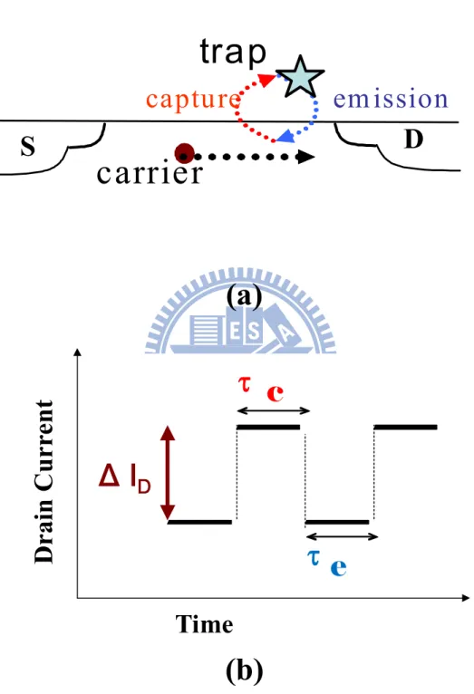
2.3 Theory of Drain Current Telegraph Noise
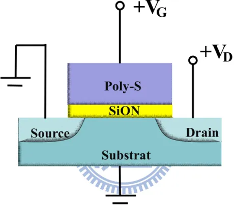
Figure 2.3(a) is the schematic showing the carrier trapping and detrapping through the oxide trap. In small devices, only trap energy within a few kT from the Fermi level would make current fluctuation where k and T are the Boltzmann constant and equilibrium temperature, respectively. So far, the drain current fluctuation is generally influenced by two effects: the number fluctuation of free channel carriers ΔNs, and the mobility fluctuation Δμ described by [2.2][2.3].
(2.1)
in the strong inversion. Here Ns is the channel carriers per unit area andα is the scattering coefficient while the sign in front of the mobility fluctuation is determined by the type of the trap (repulsive or attractive scattering center). For an acceptor type trap, the high level corresponds to the neutral state (no captured carrier) while the low level corresponds to the charged state. When the traps in the dielectric are empty and their energy level maintain at a level which is equal to that of the channel carriers or below, traps will capture carriers from the channel. When the carriers are trapped, they will increase the nearby potential and lower the current.
The three major parameters (capture time, emission time, and current amplitude) of the ID-RTN are defined in Fig. 2.3(b), capture time c is the average of the high time constants, emission time e is the average of the low time constant and current amplitude ΔID is the magnitude of the drain fluctuation. The current amplitude, capture and emission time are the critical parameters of random telegraph noise phenomenon which
] 1 [ 1 N L W N N I I d d
depend on the trap properties, such as trap depth into dielectrics, trap energy apart from conduction band (valance band if holes are captured and emitted).
Parameter Analyzer HP 4156C
PC
Probe Station
Fig. 2.1 The measurement setup using Analyzer HP 4156C to sampling as RTN
Fig. 2.2 The terminals setup for sampling by Analyzer HP4156C.
Poly-S
i
SiON
O
Source
Drain
Substrat
e
+V
G
+V
D
trap
em ission
captu re
S
D
carrier
(a)
(b)
Fig. 2.3 (a) Carrier trapping and detrapping by the slow trap near the drain
side. (b) Illustration of the three parameter of the RTN noise: capture time c, emission time e , and current amplitudeΔID.
D
ra
in
C
u
rr
en
t
Time
c
e
Δ I
D
Chapter 3
Random Telegraph Noise of Drain Current in
n-MOSFETs
3.1 Introduction
Recently, researches have shown an increasing interest in the strain technology. Strained silicon technology is essential for the continuation for the scaling of MOSFET devices, owing to its high impact on carrier mobility and thus on drive current improvement [3.1]. When applied to the direction of the channel, tensile strain improves the performance of n-MOSFET devices, while compressive strain is beneficial for p-MOSFET devices. The local strain, such as capping layer, SiGe on S/D, and SiC on S/D are induced by the process. They are usually uniaxial strain. Compared to the global strain usually biaxial strain, the local strain has less dislocation issues.
As the devices being scaled, there are plenty of reliability issues in the strained devices. Besides, trapping of a single carrier charge in traps and related local modulation in carrier density and mobility will have a profound influence in the carrier density and mobility on the drain current. The drain current fluctuation will cause serious drawbacks on the small geometry devices.
In this chapter, the ID-RTN “Drain Current Random Telegraph Noise” for the exploration of strain-induced slow trap properties is presented in strained n-MOSFETs. Single electron capture and emission could be observed. The analysis of the reliability will be introduced first in Section 3.3. Next, the analysis of drain current instability is
interpreted in Section 3.4. Based on the voltage dependence of single charge effect, the traps parameters are extracted and the strain process induced-effect will be also discussed.
3.2 Device Preparation
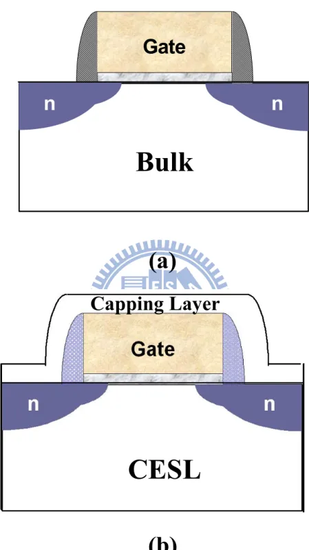
The devices were fabricated by the advanced 65nm CMOS technology at UMC. The schematic cross section diagram of n-MOSFET splits is shown in Fig. 3-1. In this figure, Fig. 3-1(a) is the bulk-Si device, and Fig. 3-1(b) is the CESL (contact etching stopping layer) capped device (uniaxial-strained). Both n-MOSFETs are <100> channel on (100) substrate. All these test devices have 14Å EOT gate oxide with SiON process and with the same dimension (W/L= 0.2/0.12um).
3.3 The Analysis of Reliability in n-MOSFETs
3.3.1 Introduction
The strain technologies can enlarge the mobility to achieve the significant driving current enhancement [3.2] [3.3] [3.4]. However, many technologies have been developed to boost the drive current; the reliability issues have been rarely studied. It is necessary to consider the effects for device characteristics involving uniaxial and biaxial strained effects for CMOS devices.
A large mobility enhancement would adversely affect the device reliability [3.5]. For n-MOSFETs, the CESL device becomes the most promising technology and the better reliability, especially with process simplicity. In 2006, S. S. Chung et al. [3.6] first
published a paper, in which they demonstrated for n-MOSFETs, tensile cap stressor device is much better in terms of reliability and performance. Based on the important results, we will further analyze the reliability issues of strain n-MOSFETs and investigate them by the ID-RTN method after hot carrier stress. They are described in two parts. The first part is to investigate hot carrier degradation and the second part is to analyze the drain current instability after HC stress in bulk-Si and CESL devices. For hot carrier degradation, threshold voltage shift, drain current degradation and transconductance degradation would be observed by electric measurement. These stresses generate the interface trap and fixed oxide charges. For the drain current instability, the stress-induced traps’ properties and the relationship between the strain and the ID-RTN results would be studied.
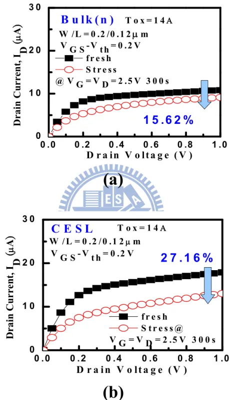
3.3.2 Drain Current Degradation
The procedure of following experiment is shown in Fig. 3.2. Firstly, in the ID-VG step, the purpose is to get the basic semiconductor parameters and make sure the devices can work successfully .Then, the devices are subjected to the ID-RTN analysis, to ensure that there is no current fluctuation in the fresh devices (i.e., no process induced traps). Then, we apply the hot carrier stress, to produce the oxide traps near the drain region which would show a two-level fluctuation of drain current. Subsequently, the ID-RTN measurement is applied to the stressed devices. Under hot carrier stress with injecting hot electrons to destruct gate dielectrics, we could prevent the effect of changing temperature and measure RTN at once. Traps generation for apparent two-level fluctuations is hard to say happening on specific time and its dependence with time on different stress voltage is also not regular. In our measurement, after HC stress (VGS= VDS= 2.5V for 300sec), we
obtain significant RTN appearance in the linear region and continued subsequent analysis. We show the ID-RTN measurement results for stressed devices and discussed the induced slow traps properties in the coming sections.
Figures 3.3 (a) and (b) show the drain current degradations before and after the HC stress. The drain current degradation in CESL device is 27.16% and in bulk is 15.62%. The CESL device shows large drain current degradation than bulk device, as result of its higher impact ionization rate (IB/ID) caused by the strain effect [3.7]. A large enhancement of the driving current will adversely degrade the device reliability.
3.4 The Analysis of I
D-RTN in n-MOSFETs
3.4.1 Drain Current WaveformThe stress induced slow oxide trap near the drain side which would cause the drain current instability (ID-RTN) through the trapping and detrapping of channel carriers. The ID-RTN measurements were performed in linear operation at a constant drain voltage VDS= 0.05V for gate voltages VGS between 0.3 - 1 V, in steps of 20mV using HP4156C. Fig. 3.4 and Fig. 3.5 show the different ID-RTN wave spectra for bulk-Si and CESL devices respectively. The drain current amplitude is about 50nA.
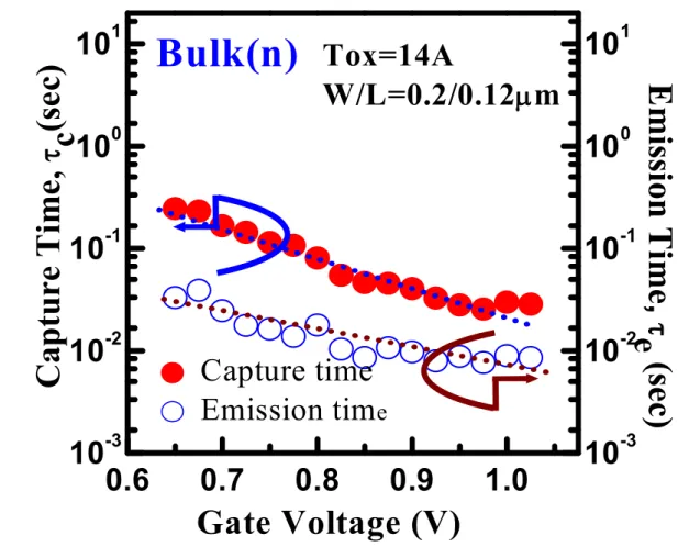
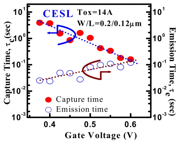
3.4.2 Capture and Emission Time
Fig. 3.6 and Fig. 3.7show the mean capture and emission time gathered statistics from Fig. 3.4 and Fig. 3.5. The decrease of c, as gate bias increases shows the acceptor type of the generated slow oxide trap [3.8]; and the capture time, c, of the slow oxide
kT
E
Bexp
0
trap in the CESL device is larger than bulk-Si device in Fig. 3.6, which implies that the trap is deeper in CESL device is larger than the bulk-Si device. The magnitudes of emission time e are both about 0.01~ 0.1 sec. While, the magnitudes of the emission time e do not show much difference. From the dependency of e, versus gate bias, the carrier in bulk-Si device detraps via Frenkel-Poole emission while carrier in CESL device detraps via trap-assisted-tunneling to the silicon substrate. Due to the thermal emission for the carrier in the bulk-silicon’s trap, the emission time decreases as gate voltage increasing in Fig. 3.6. This implies that the bulk device’s trap is near the Si/SiO2 interface. While the carrier detraps through thermally assist tunneling to the Si for CESL device, emission time increases as gate voltage increases in Fig. 3.7. Furthermore, the trapping and detrapping events happen more frequently in CESL devices so the capture time over the emission time increases more quickly in CESL than bulk device in Fig. 3.8. This also assures that the HC stress produces more damage at the Si/SiO2 for the CESL device and the trap is deeper in CESL device than bulk-Si device ones.
3.5 Discussion
According to the Shockley–Read–Hall statistics [3.9], the capture time c is sensitive to the channel carrier density n, the average carrier velocity v, and the capture cross-section as Eq. (3.1), where
(3.1) and (3.2)
nv
c1
Here, is the capture cross section. Here, 0 is the cross-section prefactor, and EB is the thermal activation energy for capture. T and v are usually taken to be the equilibrium lattice temperature and average thermal velocity vth. This approximation is invalid at large lateral electric field, and electron heating occurs and affects the electron capture time. As the gate bias increasing, the capture time would be decreased due to the increased carrier density in the channel. Emission time e is given as Eq. (3.3) [3.10],
(3.3)
where g is the degeneracy factor. The term (EF-ET) represents the trap energy with respect to the Fermi energy. kB is the Boltzmann constant.
3.5.1 Trap Depth
The relationship between the mean capture and emission times and trap parameters can be described as the following [3.11],
(3.4)
(3.5)
where ECd, EC, EF, and s are defined in Fig. 3.9. EOT is the effective oxide thickness
S FB G T S F C T Cd e c V V EOT q q E E E E kT 1 Z ln 0 EOT kT q dV d eff G e c Z ln
vn
g
T
k
E
E
F T B e
exp
/
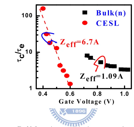
and VFB is the flat-band voltage. We can estimate Zeff, effective depth from substrate, from measurements of c/e by varying VG. The trap depth is extracted from the slope of
ln(c/e) versus VG as shown in Eq. 3.5. Zeff is 1.09A for bulk device and 6.70A for CESL device shown in Fig. 3.10. The trap in CESL is deeper than the trap in bulk-Si. The characterized depth of generated traps in Fig. 3.10 shows that CESL device will cause more fluctuations, Fig. 3.5. This also assures that HC stress produces more damage in the Si/SiO2 for the CESL and the trap location is deeper is deeper in CESL than in bulk-Si, Fig. 3.10.
3.5.2 Normalized Drain Current Amplitude
Fig. 3.11 and Fig. 3.12 show the drain current amplitude gathered statistics from Fig. 3.4 and Fig. 3.5 divided by the drain current and take plots as function of gate bias. At very low drain voltages in the strong inversion, the mobility fluctuations term Δμ/μ plays a more dominant role than the number fluctuations Δ Ns / N [3.11], i.e.,
(3.6)
Furthermore, the variation of the RTN amplitude ΔID/ID is proportional to the normalized transconductance change gm/ID ratio[3.12]
(3.7)
(i.e., ΔID/ID α gm/ID) in the bulk-Si device (Fig. 3.11); while the variation in CESL device changes rapidly (Fig. 3.12). The RTN is neither influenced by the change of
(1 ) g dID m q xT ID ID Weff eff oxL C tox 1 1 ( ) ID ID Weff Leff N
carrier fluctuation Δ Ns nor by the mobility Δμ[3.11]. Since a screened Coulomb scatter with very similarαvalues for comparable channel electron densities [3.11][3.13] , the ΔID/ID roll-off quickly in CESL device reveals that an extra carrier scattering is induced. This will give rise to an additional mobility degradation of the CESL device after the HC-stress.
Gate
n
n
(a)
(b)
Fig. 3.1 The cross-section view of the experimental devices. (a) bulk-Si and
(b) CESL (contact etching stopping layer) capped devices (uniaxial-strain). Both of them are <100> channel on (100) substrate.
Bulk
CESL
Procedure
Hot Carrier Stress
I
D-V
GI
DRTN
I
DRTN
0 . 0 0 .2 0 . 4 0 . 6 0 .8 1 . 0 0 1 0 2 0 3 0 W / L = 0 .2 / 0 . 1 2
m f r e s h S t r e s s @ V G = V D = 2 .5 V 3 0 0 s T o x = 1 4 VG S- Vt h= 0 . 2 V1 5 . 6 2 %
D
ra
in
C
u
rren
t,
I
D
(
A
)
D r a i n V o l t a g e ( V )
B u l k ( n )
0 . 0 0 . 2 0 . 4 0 .6 0 .8 1 .0 0 1 0 2 0 3 0D
ra
in
C
u
r
re
n
t,
I
D
(
A
)
D r a i n V o l t a g e ( V )
T o x = 1 4 W / L = 0 . 2 / 0 . 1 2m V G S- Vt h= 0 . 2 V f r e s h S t r e s s @ V G = V D = 2 .5 V 3 0 0 sC E S L
2 7 . 1 6 %
(a)
(b)
Fig. 3.3 The comparison of ID-VD characteristic in n-MOSFET devices
0.5 1.0 1.5 2.0 3.56 3.60 3.88 3.92 4.24 4.28 4.56 4.60 4.88 4.92 5.20 5.24 5.52 5.56 VG=0.725V VG=0.7V VG=0.75V VG=0.775V VG=0.8V D VG=0.825V VG=0.85V 5.73 5.76 5.79 VG=0.875V 6.12 6.16 VG=0.9V
Time (s)
D
rai
n
C
u
rr
en
t,
I
D
(
A
)
6.68 6.72 VG=0.95V 6.40 6.44 VG=0.925V0.5 1.0 1.5 2.0 0.82 0.84 0.86 1.08 1.10 1.12 1.38 1.40 1.42 1.72 1.74 1.76 2.08 2.10 2.12 2.48 2.50 2.52 2.90 2.92 2.94 3.36 3.38 3.40 3.82 3.84 3.86 4.32 4.34 4.36 4.82 4.84 4.86 VG=0.6V VG=0.625V VG=0.65V VG=0.675V VG=0.7V VG=0.5V VG=0.45V VG=0.475V VG=0.525V VG=0.55V VG=0.575V
D
ra
in
C
u
rr
en
t,
I
D
(
A
)
Time (s)
0.6
0.7
0.8
0.9
1.0
10
-310
-210
-110
010
1Gate Voltage (V)
C
a
p
tu
re
T
ime
,
c(
se
c)
10
-310
-210
-110
010
1E
mi
ss
io
n
T
ime
,
e
(s
ec
)
Tox=14A
W/L=0.2/0.12
m
Capture time
Emission tim
e
Bulk(n)
Fig. 3.6 Variation of capture time c (filled symbol) and emission time e (open symbol) as gate voltage increases for bulk-Si device.
0.4
0.5
0.6
10
-310
-210
-110
010
110
-310
-210
-110
010
1C
a
pt
u
r
e
T
im
e
,
c
(s
ec
)
Gate Voltage (V)
Tox=14A
W /L =0.2/0.12
m
Capture time
Emission time
C ESL
E
m
is
sio
n
T
im
e
,
e
(
se
c
)
Fig. 3.7 Variation of capture time c (filled symbol) and emission time e (open symbol) as gate voltage increases for CESL device.
0.4
0.6
0.8
1.0
1
10
100
c
/
e
G a te V o ltag e (V )
B u lk (n )
C E S L
Z eff=6.7A
Z eff=1.09A
Fig. 3.8 Capture time over emission time versus gate voltage plots for
Fig. 3.9 Energy band diagram at the trap position in the channel.
Ec
Ev
E
FE
Cd-
E
TZ
effE
Fg CgTrap
Channel
Dielectric
Gate
φ
0
q
Ψ
S(a)
(b)
Fig. 3.10 The effective depth location for the two traps in, (a) bulk-Si and (b)
CESL devices.
6.7Α
Trap
Channel
Dielectric
Gate
1.09Α
Trap
Channel
Dielectric
Gate
0.6
0.7
0.8
0.9
1.0
0.00
0.02
0.04
Tox=14A
W/L=0.2/0.12
m
VDS=0.05V
Bulk(n)
I D
/I
D
g
m/I
D I
D/I
DGate Voltage (V)
Fig. 3.11 Normalized RTN amplitude (filled symbol) and normalized
conductance change (open symbol) versus gate voltage for bulk-Si device.
0.4
0.5
0.6
0.7
gm/ID
I
D /I
DT ox=14A
W /L =0.2/0.12
m
V
DS=0.05V
C E SL
I D
/I
D
G ate V oltage (V )
Fig. 3.12 Normalized RTN amplitude (filled symbol) and normalized
conductance change (open symbol) versus gate voltage for bulk-Si device.
Chapter 4
Random Telegraph Noise of Drain Current in
p-MOSFETs
4.1 Introduction
Mobility enhancement is a method to improve the CMOS devices performance with the scaling of the device size. The increase of carrier mobility is necessary to realize the high-speed CMOS devices. Recently, various strain technology have been utilized to enhance the drive current. It is necessary to understand the introduced uniaxial and biaxial strains in n-MOSFET or p-MOSFET devices. Initially, the typical mobility enhancement of n-type strained-Si is much larger than that of p-type devices. Several techniques have been further developed to enhance the p-MOSFET performance, i.e., SiGe on S/D device [4.1]. Materials with same crystal structure but different lattice are good candidates for strain engineering. The SiGe has been successfully incorporated in the source and drain of p-MOSFET devices to strain the channel compressively and increase the hole mobility. Furthermore, trapping of a single carrier charge in traps and related local modulation in carrier density and mobility exhibit a profound influence in the carrier density and mobility on the drain current. The drain current fluctuation will cause serious drawbacks on the small geometry devices.
In this chapter, the ID-RTN “Drain Current Random Telegraph Noise” for the exploration of strain-induced slow trap properties is presented. Single electron capture and emission could be observed in strained p-MOSFETs. The analysis of the reliability will be introduced first in Section 4.3. Next, the analysis of drain current instability is
interpreted in Section 4.4. Based on the voltage dependence of single charge effect, the traps parameters are extracted and the strain process induced-effect will also be explained.
4.2 Device Preparation
The schematic cross sections of p-MOSFET splits are shown in Fig. 4-1. In this figure, Fig. 4-1(a) is the bulk-Si device, and Fig. 4-1(b) is the SiGe on source/drain device (uniaxial-strain) with EDB (Embedded Diffusion Barrier). Both p-MOSFETs are <110> channel on (100) substrate. All these test devices have 14Å EOT of SiON gate oxide and with the same dimensions, W/L = 0.2/0.12 μm. The ID-RTN was investigated in bulk and SiGe on S/D pMOSFET devices fabricated using a conventional CMOS process flow.
4.3 The Analysis of Reliability in p-MOSFETs
4.3.1 Introduction
For many strained approach to enhance the carrier mobility, the reliabilities are still a serious issue. The biaxial strained SiGe-channel device provides good drive current enhancement, it suffers from the Ge-outdiffusion such that exhibits worse reliability. The SiGe on S/D device is a promising structure for p-MOSFET design since it keeps at about the same reliability as the SiGe-channel ones while exhibits a much higher performance. In contrast, SiGe-channel has a major concern with lattice misfit [4.2]. Besides, for p-MOSFET devices, the SiGe on S/D device with EDB [4.3] is the most promising in terms of performance and reliability.
In this section, we analyze the reliabilities of strained p-MOSFET devices and investigate them by the ID-RTN method after hot carrier stress. We divide the contents into two main sections. The first part is to investigate hot carrier degradation and the second part is to analyze the drain current instability for p-MOSFETs. In hot carrier degradation, threshold voltage shift, drain current degradation, and transconductance degradation would be observed by electric measurement. These stresses generate the interface trap and fixed oxide charges. For the drain current instability, the stress-induced traps’ properties and the relationship between the strain and the ID-RTN results would be understood. Finally, the comparison for the strained n- and p-MOSFETs would be discussed according to the previous result.
4.3.2 Drain Current Degradation
Similar experimental procedures have been conducted for SiGe S/D device and bulk-Si p-MOSFET devices. After the hot carrier stress (VGS=VDS= -2.5V 300sec), Figs. 4.2 (a) and (b) show that the drain current degradation before and after the HC-stress. The drain current degradation in SiGe on S/D device is 16% and in bulk-Si device is 7.44%. The SiGe on S/D device shows large drain current degradation than bulk device, resulting from its higher impact ionization caused by the strain and the Ge out-diffusion [4.4]. The SiGe on S/D device has a larger impact ionization rate and Ge out-diffusion near the drain region which gives rise to larger drain current degradation than bulk device, caused by the impact ionization rate, the SiGe on S/D devices have a worse ID degradation, i.e., worse immunity for hot-carrier stress.
4.4 The Analysis of I
D-RTN in p-MOSFETs
4.4.1 Drain Current WaveformThe stress induced slow oxide trap near the drain side which would cause the drain current instability (ID-RTN) through trapping and detrapping the carriers in channel. The ID-RTN measurements were performed in linear operation at a constant drain voltage VDS= -0.05V for gate voltages |VGS| between 0.3 - 1 V, in steps of 20mV using HP4156. Fig. 4.3 and Fig. 4.4 show the different ID-RTN wave spectra for bulk-Si and SiGe on S/D device respectively. The drain current amplitude is about 50nA.
4.4.2 Capture and Emission Time
From Fig. 4.3 and Fig. 4.4, we analyzed the capture and emission time for the two devices. In Fig. 4.5 and Fig. 4.6, as the gate bias increases, the capture time, c decreased due to a larger carrier concentration in the channel. While the emission time, e decreased with increasing gate bias which means that the carrier detraps through thermally assist tunneling to the Si. The magnitudes of c and e are both about 0.01~0.1 sec.As a result, both devices show similar behavior of the capture and emission of holes.
4.5 Discussion
4.5.1 Trap Depth
The relationship between the mean capture and emission times and trap parameters can be described as Eq. 3.4. The trap depth is extracted from the slope of ln(c/e) versus VG as shown in Eq. 3.5. Zeff is 9.59A for bulk-Si device and 10.39A for SiGe on S/D
device shown in Fig. 4.7. Also, the depths of generated oxide traps location are about the same (~10A) in Fig. 4.8 for both devices so the capture time over the emission time take no difference in the two oxide traps (Fig. 4.7).
4.5.2 Normalized Drain Current Amplitude
The normalized change of the ID-RTN amplitude is proportional to the normalized conduction change for both devices (Fig. 4.9 and Fig. 4.10). This implies that the generated slow oxide trap in SiGe on S/D follows the same mechanism as that of bulk device.
4.6 The Comparison Between n- and p-MOSFETs
4.6.1 Introduction
The hot carrier degradation of the CMOS devices with various strain technologies were enhanced by high lateral acceleration and larger impact ionization current. The worst case of hot carrier degradation occurs at VGS= VDS condition and the degradation will follow the trend of impact ionization rate and effective mobility. In addition to the discussion on the reliabilities of uniaxial strained CMOS devices, for the first time, the ID-RTN for the strained-Si devices is analyzed. In order to identify the differences of previous experimental results, the strain effects in CESL device and SiGe on S/D devicecan be identified by Fig. 4.11. The capping layer in the n-MOSFET devices provides the tensile strain along the channel direction and also the compressive strain along the vertical direction [4.5]. The SiGe on S/D devices inducing the compressive strain along the channel region gives rise to the hole mobility enhancement.
4.6.2 Charge Pumping Measurement
The charge pumping (CP) measurement is efficient for the reliability characterization. However, the charge pumping measurement can’t be used reliably in the small size devices due to the small charge pumping current and the gate leakage current. Recently a low leakage IFCP measurement for COMS devices has been developed [4.6] to get more reliable results. In order to investigate the interface’s degradation information, we used the low leakage IFCP measurement for the stressed devices.
4.6.2.1 Experimental Results
We took charge pumping measurements which can be used to calculate the information of the degradation for the interface only. As a figure of merit, in Fig. 4.12, for the comparison the degradation caused by the interface 1.26 times larger in CESL device than in bulk-Si device, while the ID degradation shows a factor of 1.69 times larger for CESL device comparing to the bulk-Si device in Fig. 4.13 .
As a result, the difference of 1.69 and 1.26 will give a difference of 0.43 times of the total drain current degradation. This is the contribution from the strain in the vertical direction as show in Fig. 4.11.
4.6.3 ID-RTN: Normalized Drain Current Amplitude
(normalized current amplitude) should be proportional to the mobility [4.7]. From Fig. 4.14, the ΔID/ID roll-off more quickly in the CESL device compared to the bulk-Si device, while the SiGe on S/D device and bulk-Si device show comparable trend. Because of the extra vertical strains in the CESL device gate dielectric (Fig. 4.11), this would cause more scattering and degrade the Si/SiO2 interface quality after the HC stress.
4.6.4 Discussion
The vertical strain on the gate oxide causes higher mobility degradation in CESL device than bulk-Si device, in poly-Si gated devices. We believe that the drain current degradation between n-MOSFET and p-MOSFET could be due to the extra strain stress on the gate dielectric.
The vertical strain causes about 0.43 times of the total drain current degradation (~one-quarter of the total degradation). As a result: (1) the strain techniques can enhance the device performance while on the contrary they show poorer got carrier reliabilities, (2) more scattering is induced by the CESL strain (as observed in n-MOSFET) which can induce the mobility degradation and make worse the device reliability.
Gate
p
p
Gate
SiGe
SiGe
(a)
(b)
Fig. 4.1 The cross-section view of the experimental devices, (a) bulk-Si and
(b) SiGe on S/D device (biaxial-strain). Both of them are <110> channel on (100) substrate.
Bulk
0 .0
- 0 .2
- 0 .4
- 0 .6
-0 .8
- 1 .0
0
2
4
6
8
T o x = 1 4 A
B u l k ( P )
D
ra
in
C
ur
r
ent
,
I D
(
A
)
D r a i n V o lt a g e , V
D( V )
f r e s h
S t r e s s @
V
G= V
D= 2 . 5 V , 3 0 0 s
W /L = 0 . 2 / 0 . 1 2
m
V G S -V th = 0 .2 V
7 . 4 4 %
0 .0
-0 .5
-1 .0
0
4
8
T o x = 1 4 A
W /L = 0 .2 /0 .1 2
m
S iG e S /D
V
G S
- V
th
= 0 .2 V
fr e s h
S tr e s s @
V
G= V
D= -2 .5 V ,3 0 0 s e c
1 6 %
D
r
a
in
C
u
rr
en
t,
I
D
(
A
)
D r a in V o lt a g e , V
D( V )
(a)
(b)
Fig. 4.2 The comparison of ID-VD characteristic in p-MOSFET devices
4.2 4.4 4.6 4.8 5.0 5.2 1.12 1.16 1.71 1.74 2.40 2.44 3.20 3.24 4.12 4.16 5.08 5.12 VG=0.375V VG=0.4V VG=0.425V VG=0.45V VG=0.475V VG=0.5V
Time (s)
D
ra
in
C
u
rr
en
t,
I
D
(
A
)
1
0
3.00 3.05 3.10 3.85 3.90 3.95 4.75 4.80 4.85 5.70 5.75 5.80 6.70 6.75 VG=0.425V VG=0.45V VG=0.475V VG=0.5V VG=0.525V
Time (s)
D
r
a
in
C
u
r
re
n
t, I
D
(
A
)
1
0
3.0 3.2 3.4 3.6 3.8 4.0 2.25 2.30 2.35 VG=0.4V0.35
0.40
0.45
10
-310
-210
-110
0Gate Voltage, VG (-V)
C
a
p
tu
r
e
Ti
m
e
,
c(s
ec)
10
-310
-210
-110
0E
m
is
si
o
n
T
im
e
,
e
(s
ec
)
Tox=14A
W/L=0.2/0.12
m
Capture time
Emission time
Bulk(P)
Fig. 4.5 Variation of capture time c (filled symbol) and emission time e (open symbol) as gate voltage increases for bulk-Si device.
0.35
0.40
0.45
10
-310
-210
-110
0Capture time
Emission time
10
-310
-210
-110
0SiGe S/D
Tox=14A
W/L=0.2/0.12
m
E
mi
ss
io
n
T
ime
,
e(s
e
c)
10
10
10
10
C
a
pt
ur
e
T
im
e
,
c
(s
e
c
)
Fig. 4.6 Variation of capture time c (filled symbol) and emission time e (open symbol) as gate voltage increases for SiGe on S/D device.
0.36
0.40
0.44
0.48
0.1
1
10
c
/
e
Gate Voltage, V
G
(-V)
SiG e
Bulk
Zeff=9.59A
Z
eff
=10.39A
Fig. 4.7 Capture time over emission time versus gate voltage plots for
(a)
(b)
Fig. 4.8 The effective depth location for the two traps in, (a) bulk-Si and
(b) SiGe on S/D devices.
10.39Α
Trap
Channel
Dielectric
Gate
9.59Α
Trap
Channel
Dielectric
Gate
0.35
0.40
0.45
0.00
0.01
0.02
ID/ID
gm/ID
I
D
/I
D
Tox=14A
W /L=0.2/0.12
m
VDS=0.05mV
Gate Voltage, V
G
(-V)
Bulk(P)
Fig. 4.9 Normalized RTN amplitude (filled symbol) and normalized
conductance change (open symbol) versus gate voltage for bulk-Si device.
0.35
0.40
0.45
0.00
0.01
0.02
0.03
W/L=0.2/0.12
m
VDS=0.05mV
SiGe S/D
ID/ID
gm/ID
Tox=14A
Gate Voltage, V
G(-V)
I
D
/I
D
Fig. 4.10 Normalized RTN amplitude (filled symbol) and normalized
conductance change (open symbol) versus gate voltage for SiGe on S/D device.
tensile stress
compressive
stress
D
S
CESL
Capping layer
compressive stress
SiGe on S/D
D
S
(a) (b)Fig. 4.11 Illustration of the various strains for (a) CESL and (b) SiGe on S/D
-0.5
0.0
0.5
1.0
0.0
10.0p
20.0p
30.0p
I c
p
(
A
)
Gate Voltage,V
gh
(V)
Bulk_stress
Bulk_fresh
CESL_stress
CESL_fresh
1300%
1032%
1.26
Fig. 4.12 Comparison of charge pumping current for bulk-Si and CESL
0.0
0.2
0.4
0.6
0.8
1.0
0
5
10
15
20
D
rain
C
u
rr
e
n
t,
I
D
(
A
)
D ra in V o lta g e, V
D(V )
C E S L_ fresh
C E S L _ stress
B u lk_ fresh
B u lk_ stress
27%
16%
1.69
Fig. 4.13 Comparison of drain current degradation for bulk-Si and CESL
0.0
0.2
0.4
0.6
0.01
0.02
0.03
0.04
I
D
/I
D
|V
G-V
th|
Bulk(n)
CESL
-0.1
0.0
0.1
0.2
0.3
|V
G-V
th|
SiGe S/D
bulk(P)
Fig. 4.14 Normalized current amplitude versus overdrive voltage. (left)
n-MOSFETs (right) p-MOSFETs. Note that the huge drop for CESL device is caused by the vertical strain in CESL device.
Chapter 5
Application to Strained SiC Devices
5.1 Introduction
Strained silicon channel has become an essential component of modern high-performance CMOS technology. In order to overcome the MOSFET device scaling difficulties, various strained-Si schemes have become essential components for 45 nm and beyond. Recently, strained n-MOSFET with embedded Si:C on source and drain has received much interest owing to its good scalability for gate length small than 40nm [5.1]. With the same lattice constant that is smaller than Si, silicon carbon alloy (Si:C) embedded in the source and drain can provide tensile strain along the channel direction and enhance the electron mobility for n-MOSFET. The SiC on S/D is a superior stressor compared to SMT and shows better scalability for high performance thin-oxide short channel n-MOSFET [5.2] [5.3].
In this chapter, the application to the SiC device would be illustrated by the ID-RTN method. The experiment results would also be discussed and compared with the pervious chapters’ result.
.
5.2 Device Preparation
The devices were fabricated by the advanced 40nm technology. The schematic cross section diagram of n-MOSFET splits is shown in Fig. 5-1. In this figure, Fig. 5-1(a) is the bulk-Si device, and Fig. 5-1(b) is the SiC on S/D device (uniaxial-strain). Both