國立交通大學
電子工程學系 電子研究所碩士班
碩 士 論 文
以備用標準單元實現工程變更
之邏輯合成
Logic Resynthesis with Spare Cells for
ECO Consideration
研 究 生:洪煌筆
指導教授:江蕙如 博士
以備用標準單元實現工程變更之邏輯合成
Logic Resynthesis with Spare Cells for ECO Consideration
研究生:洪煌筆
Student: Huang-Bi Hong
指導教授:江蕙如 博士
Advisor: Dr. Iris Hui-Ru Jiang
國 立 交 通 大 學
電子工程學系電子研究所碩士班
碩 士 論 文
A Thesis
Submitted to Department of Electronics Engineering & Institute of Electronics College of Electrical and Computer Engineering
National Chiao Tung University in Partial Fulfillment of the Requirements
for the Degree of Master
in
Electronics Engineering July 2009
Hsinchu, Taiwan, Republic of China 中華民國 九十八年七月
iii
以備用標準單元實現工程變更之邏輯合成
研究生 : 洪煌筆 指導教授 : 江蕙如 博士
國立交通大學
電子工程學系 電子研究所
摘 要
Engineering Change Order (ECO)指的是在標準設計流程外對原始設計中元 件或規格做修正,為目前晶片設計產業面臨的重要議題。隨著晶片設計日益複雜, 晶片設計過程不時有修正設計的需求。同時,晶片設計產業的激烈競爭使得 time-to-market 的壓力更勝以往。為了節省時間,晶片設計者必需以手動的方式 修正錯誤或是規格的變更。然而,手動的修改效率低落而且修正的品質不佳。另 一方面,光罩的成本也隨著製程增加,就成本的考量,metal-only ECO 固定了 base layer,設計者只能修正 metal layer,可以大幅地降低修改光罩的成本。
本篇論文就 post-silicon 階段的 metal-only ECO 建立了一個自動化合成的系 統。給定一個包含實體資訊的設計以及需要執行 ECO 的清單,這個系統會根據 實體設計中所包含的 spare cells 所提供的 cell types 逐一替換 ECO list,同時最小 化替換過程中所增加的連線複雜度。本篇論文的特點在於這個系統融合了既有的 合成系統並且考慮了實體資訊,有效的自動化 ECO 的需求。
iv
Logic Resynthesis with Spare Cells for
ECO Consideration
Student: Huang-Bi Hong
Advisor: Dr. Iris Hui-Ru Jiang
Department of Electronics Engineering
Institute of Electronics
National Chiao Tung University
Abstract
ECO is the process of inserting a logic change directly into the netlist to fix functionality or timing violation. It is prevalent for saving either time or cost. Before the manufacture of masks, ECOs save time by avoiding re-building from scratch. On the other hand, metal-only ECO can save time and reduce the cost after the photomaks have been made. It implements incremental design changes using spare cells sprinkled at placement stage. Metal-only ECO realizes the last-minute design changes by revising the photomasks of metal layer only, the photomasks of base layer can be reuse in the next tape-out. ECO is desirable; however, there are rare automatic tools and engineers have to implement ECO manually.
In this thesis, we propose an ECO resynthesis methodology, named Guided ABC, that correctly implements the incremental design changes using the available spare cells as well as tries to reduce the prohibitive photomask cost at the same time. The experiments are conducted on five industrial testcases. Guided ABC uses less wirelength and/or fewer cells to complete design changes for all cases than the blind method that synthesizes the ECOs with available spare cell types directly.
v
Acknowledgements
I would like to express my heartfelt gratitude to my advisor, Prof. Iris Hui-Ru Jiang, for her guidance and spur throughout my graduate course. Then, I would like to be grateful to the members of my thesis committee, Dr. Evan Yu-Wen Tsai and Prof. Mango Chia-Tso Chao, for their precious suggestions and comments. Meanwhile, I deeply appreciate Liang-Gi, my best partner and members of IRIS Lab, Wan-Yu, Yen-Ting, Yu-Ming, Cheng-Chi and May. Also, I appreciate my friends from NCHU. For their kindly help and encouragements, I could break through my research bottlenecks and share my interesting life. Finally, I display my warmest appreciation to my mother for her love and consideration.
Huang-Bi Hong
National Chiao Tung University July 2009
vi
Table of Contents
Abstract (Chinese) i Abstract ii Acknowledgements iii List of Tables viList of Figures vii
Chapter 1 Introduction 1
1.1 Background ... 1
1.2 Previous Work ... 4
1.2.1 ECO Compiler ... 4
1.2.2 Spare Cells with Constant Insertion ... 5
1.2.3 Timing ECO ... 5
1.3 Contribution ... 7
1.4 Thesis Organization ... 8
Chapter 2 Preliminaries and Problem Formulation 9 2.1 Preliminaries ... 9
2.1.1 Binary Decision Diagram ... 9
2.1.2 And Inverter Graph ... 9
2.1.3 NPN-class ... 10
2.1.4 Technology Mapping ... 11
2.1.5 DFS Algorithm... 16
2.2 Problem Formulation ... 16
Chapter 3 Our Algorithm 17 3.1 Guided ABC... 18
3.1.1 Library Cells Grouping ... 18
vii
3.1.3 Cell Mapping ... 19 3.1.4 Mapping Strategy ... 22 3.2 Spare Cell Selection: Stable Matching ... 22
Chapter 4 Experimental Results 24
Chapter 5 Conclusion 28
5.1 Concluding Remarks ... 28
viii
List of Tables
4.1 Statistics on testcases and on ECO... 24 4.2 Comparison on total cost. ... 25
ix
List of Figures
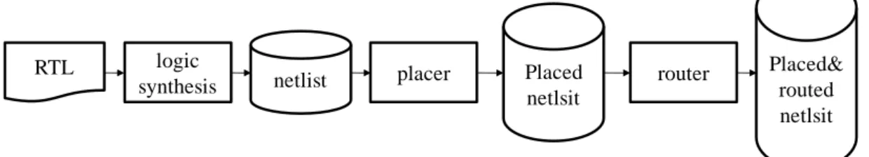
1.1 Typical ASIC flow ... 1
1.2 (a) Fucntional ECO. (b) Timing ECO ... 2
1.3 ECO compiler flow ... 4
1.4 Constant insertion for AOI21 cell ... 5
1.5 Timing ECO: (a) Timing violation. (b) Gate sizing. (c) Buffer insertion ... 6
2.1 F = B (A+C): (a)BDD implementation. (b) AIG implementation ... 10
2.2 Network covering: (a) Simple network. (b) Using one gate per vertex. (c) Network cover with library cells including 2-input and 3-input AND and OR gates. (d) Alternative network cover... 12
2.3 The DAGON approach ... 12
2.4 Pseudo-code of the technology mapping flow ... 14
2.5 Different AIG structure for function F = abc ... 15
2.6 Two cases of AIG rewriting of a node ... 15
3.1 The overview of ECOS ... 17
3.2 Detailed guided ABC ... 18
3.3 Example for ECO list partitioning ... 19
3.4 (a) Original design. (b) Bounding box including SPARE1. (c) Bounding box including SPARE2... 21
3.5 Mapping strategy ... 22
4.1 Placement of testcase4 ... 26
1
Chapter 1
Introduction
1.1
Background
隨著製程的進步,晶片需要處理的功能越來越多,使得晶片設計複雜度與日 俱增。然而在 Electronic Design Automation (EDA)的輔助下,晶片設計者得以致 力於晶片功能的研發。為了加速晶片設計的開發,已發展出一套標準流程,如 Figure 1.1(a)。 雖然有 EDA 工具的輔助,晶片設計的過程中還是會出現與規格相異的問題。 另一方面,在電子產品汰換迅速的時代,為了適應市場的需求,臨時的規格修改 亦是在所難免。在傳統的設計流程中,當原始的設計需要修正時,就必需回頭修 改硬體描述語言,並重新執行合成、測試及實體設計等步驟。 然而,在晶片設計業界的激烈競爭中,time-to-market 的壓力卻更勝以往。除了 標準設計流程中每個步驟,其中每個環節之間的驗証所需要的時間也隨著設計的 複雜度而增加。以上這些因素造就了 Engineering Change Order (ECO)的研究。 ECO 是指在標準設計流程外對原始設計做修正的程序,可以快速的修正設計以 符合設計規格。一旦設計遇到上面所描述的情形而需要修正,為了減輕上市時機 的壓力,晶片設計者會選擇從目前的階段直接修正,而不是重頭執行合成、實體 設計等環節。ECO 可以用在 function 以及 timing 的修正[8][9][10],如 Figure
Figure 1.1: Typical ASIC flow.
RTL Placed router
netlsit logic
synthesis netlist placer
Placed& routed netlsit
2
1.2(a),ECO1 (AND)替換 U3 (OR),完成 functional change;Figure 1.2(b),U3 與 out 形成 critical path,在中間插入一個 buffer 以修正 timing。在設計流程中的每 個階段都可以執行 ECO,但是在越後段執行,面臨的挑戰也會越大。
製程的進步提升了效能同時也提升了光罩(photomask)的成本,當製程進入到 奈米世代,完整的光罩組的成本也許超過一百萬美金[1]。如果在做完光罩或是 產品上市以後才發現到需要修正的錯誤或是規格的變更,重新製作光罩的成本將 會是沉重的負擔。Metal-only ECO 可以降低修正光罩的成本,藉由固定 base layer, 設計者只能修正設計中的繞線。由此,只有金屬層的光罩需要更新,將可大幅節 省成本。另一方面,由於 base layer 沒有改變,這個部分的光罩可以先行製作, 縮短設計的時間。 (a) (b)
Figure 1.2: (a) Fucntional ECO. (b) Timing ECO.
ECO1 in1 in2 U1 U2 U3 U4 in1 in2 net2 net3 net1 out2 out1 out1 SPARE3 SPARE1 out in1 in2 U1 U2 U3 in1 in2
3
想要有效的實現 metal-only ECO 需要有賴以下條件。
1. Sufficient and evenly sprinkled spare cells:為了讓 ECO 在晶片上的每個位 置都可以進行,當設計來到擺置(placement)的階段時,必頇在上面均勻地 埋入 spare cells。另外,為了避免訊號浮接,這些 spare cells 的輸入都會 接到邏輯壹或是邏輯零。接著,當 ECO 被執行時,適合的 spare cells 會 被選擇,其輸入與輸出也會被接到相對應的連線。
2. A good ECO-router:Metal-only ECO 會改變 nets 的連線狀態,重新繞線 時需要考慮以下問題。(a) timing violation:一條 net 所驅動的 cells 可能增 加,造成 delay 增加。(b) existing obstacles and various design rules:原始 設計中存在著運作正常的 nets,它們不能被更動。另外,還需要考慮訊 號傳遞時對其周圍的線路造成的影響。因此,ECO routing 所能使用的資 源相當有限[6][7]。
3. Powerful ECO synthesizer:ECO synthesizer 在實現 functionality/timing changes 的同時,必頇考慮實體資訊並正確的建立 spare cells 對於光罩 cost 的影響的模型,使得 cost 可以有效地被減少。
4
1.2
Previous Work
這個章節將會介紹前人所做的研究成果。ECO 的需求在設計環節中都可能 出現。以下將會介紹在不同階段的研究執行 ECO 的研究。1.2.1 ECO Compiler
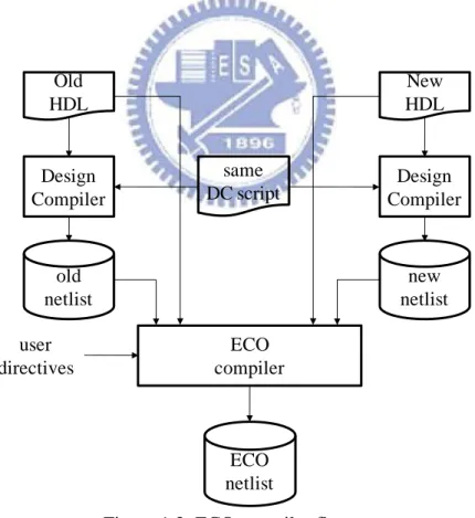
ECO compiler [3]提供 RTL 層級的修正功能,給定修正後的 RTL 程式碼,首 先要求 design compiler 以相同的參數合成出新的 netlist,接著 ECO compiler 會比 對原始與修正過的 netlists 之間的差異並寫成 ECO netlist。然而 ECO compiler 並 沒有將實體資訊納入考量,設計者仍需以手工的方式以 spare cells 完成 ECO list 或是重新擺置修正過的 netlist。使得 ECO compiler 未能確切符合產業界的需求, Figure 1.3。Figure 1.3: ECO compiler flow.
New HDL Old HDL Design Compiler Design Compiler new netlist old netlist ECO compiler ECO netlist same DC script user directives
5
1.2.2 Spare Cells with Constant Insertion
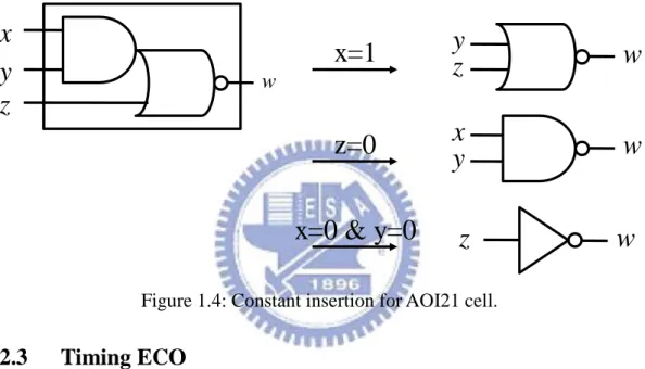
不同於標準流程的合成,spare cells 有數量及種類的限制。因此 Kuo [9]提出 constant insertion 的概念增加 spare cells 在使用上的彈性。當 ECO 無法找到相同 種類的 spare cells 時,藉由將 cells 的輸入固定至邏輯壹或邏輯零,便可由其它種 類的 spare cells 實現 ECO 的需求。如 Figure 1.4 所示,AOI21 可用來執行 NOR2、 NAND2 或是 INVERTER。接著根據 ECO 所需要的功能及 spare cells 建立 flow graph,再以 maximum flow minimum cost 找出適合的 spare cells 實現 ECO。
Figure 1.4: Constant insertion for AOI21 cell.
1.2.3 Timing ECO
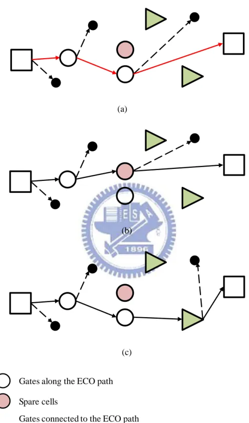
Timing violation 為 晶 片 設 計 上 常 見 之 問 題 , 常 見 的 解 決 方 法 為 buffer insertion 及 gate sizing。在 post-silicon 之後,Chen [8]提出以 spare cells 改善 timing 的演算法,將 static timing analysis (STA)所發現的 critical paths 逐一修正,Figure 1.5(a)。由於 spare cells 有數量的限制,ECOs 之間也有爭搶同一個 spare cell 的狀 況,這篇論文以動態規劃(dynamic programming)找出最適合的 buffers 以修正 timing。
y
y
z
x
wx
w
z
y
w
z
w
z=0
x=0 & y=0
x=1
6 (a)
(b)
(c)
Figure 1.5: Timing ECO: (a) Timing violation. (b) Gate sizing. (c) Buffer insertion. Gates along the ECO path
Spare cells
7
1.3
Contribution
本 篇 論 文 提 出 了 一 個 在 post-layout 的 階 段 , 考 慮 到 實 體 設 計 的 ECO resynthesizer。當 ECO 需要被執行時,根據擺置階段事先埋藏的 spare cells 替換 需要被修正的電路,並考慮 spare cells 在實體設計中的坐標,使得執行 ECO 所 額外增加的連線長度為最小。
本篇論文具有以下幾項特點:
1. Integrating physical information into resynthesis: 在整個 resynthesis 的過程
中,所有 cells 在擺置中的位置會被視為最佳化的重要參考。
2. Minimizing the photomask cost: ECO 的過程會考量所有 cells 在擺置上的位
置,避免 ECO 挑選到太遠的 spare cells,使得 ECO 可以達到最小的 cost, 進而減少修正光罩的成本。
3. Handling non-tree type spare cells and ECO functions: Non-tree type cell 像
是多工器(multiplexer)可以在這個系統被利用。
4. Considering constant value insertion for spare cells: Constant insertion 的概
念被用來增加 spare cells 使用的彈性。
5. Recycling free-up cells for subsequent ECO runs: ECO 所釋放出來的 cells 會
被回收,並且可以被後續的 ECO 當作 spare cells 使用。
6. Extending to timing ECO: 當使用者知道修正 timing 需要插入多少個 buffer
或是以其它 spare cells 取代時,將這些資訊寫入 ECO list,便可以利用這個 系統完成 timing 的修正。
我們以 5 個 benchmarks 做為實驗的對象。相較於 direct 只考慮 spare cell types, ECOS 考慮了 spare cell 的坐標及數量,ECOS 所產生的結果,在搭配了 stable matching 後,cost 只有 direct 的 95%;half-perimeter bounding box (HPBB)只有 direct 的 53%。程式的執行時間仍然相當短。
8
1.4
Thesis Organization
本篇論文將在第二章介紹預備知識以及描述問題的定義;第三章詳述本篇 論文的演算法;第四章將會分析實驗結果; 第五章會總結此論文以及未來研究方 向。
9
Chapter 2
Preliminaries and Problem Formulation
2.1
Preliminaries
這個章節將會介紹本篇論文所研究的研究知識,以及相關的問題定義。
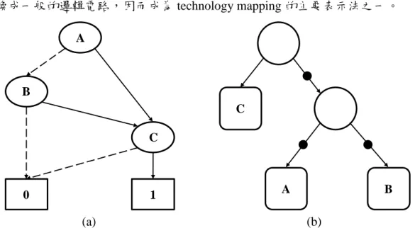
2.1.1 Binary Decision Diagram
Binary decision diagram (BDD) [19]是 boolean function 的表示法之一,是一種 directed acyclic graph (DAG) 。 包 含 decision nodes 及 terminal nodes: 0-terminal/1-terminal。每個 Decision nodes 代表一個變數,並有兩個 child nodes: low/high child,Figure 2.1(a)。一條 edge 從 node 指向其 low (high) child,代表 node 的值為 0 (1)。Figure 2.1(a),node A 經由虛線指向 node B,表示 node B 為 node A 之 low child;node A 經由實線指向 node C,表示 node C 是 node A 的 high child。 從 root 到 terminal 所經過的路線會反應變數的組合,舉例來說,Figure 2.1(a)中 node A 經由虛線到 node B (A = 0),node B 再經由實線到 node C (B = 1),node C 再由實線到 1-terminal (C = 1),代表(A, B ,C) = (1, 0, 1)會使得 F = B (A+C)為 1。 BDD 變數的順序會影響 node 的數目,node 數量越少需要的資源越少。BDD 可 以直接將其中的 node 以多工器取代,但是要轉換成一般的邏輯電路,需要額外 的計算。以下將介紹另一個架構簡單而且有效率的表示法。
2.1.2 And Inverter Graph
And-inverter graph (AIG) [18]也是一種 DAG,同樣是 boolean function 的表示 法之一,其中的節點可能有零或兩個輸入。如果一個節點沒有輸入,此節點就是 primary input;如果節點有兩個輸入,此節點即代表一個 two-input AND。Inverter 的特性由 edge 呈現,當 edge 標示為反向時,代表經由這個 edge 的訊號會遇到 一個 inverter,Figure 2.1(b)。相較於 BDD,AIG 可以透過 De Morgan's laws 直接
10
轉換成一般的邏輯電路,因而成為 technology mapping 的主要表示法之一。
(a) (b)
Figure 2.1: F = B (A+C). (a)BDD implementation. (b) AIG implementation.
2.1.3 NPN-class
兩個 boolean function F、G。如果經由反轉(Negating)並交換(Permuting)F 的 輸入然後再反轉(Negating)輸出,可以得到與 G 相同的結果,F、G 即屬於相同 NPN-class。舉例來說,F = ab + c、G = ac + b,交換 b c 可使得 F = G,F、G 即 屬於相同 NPN-class。 A B C 0 1 A B C
11
2.1.4 Technology Mapping
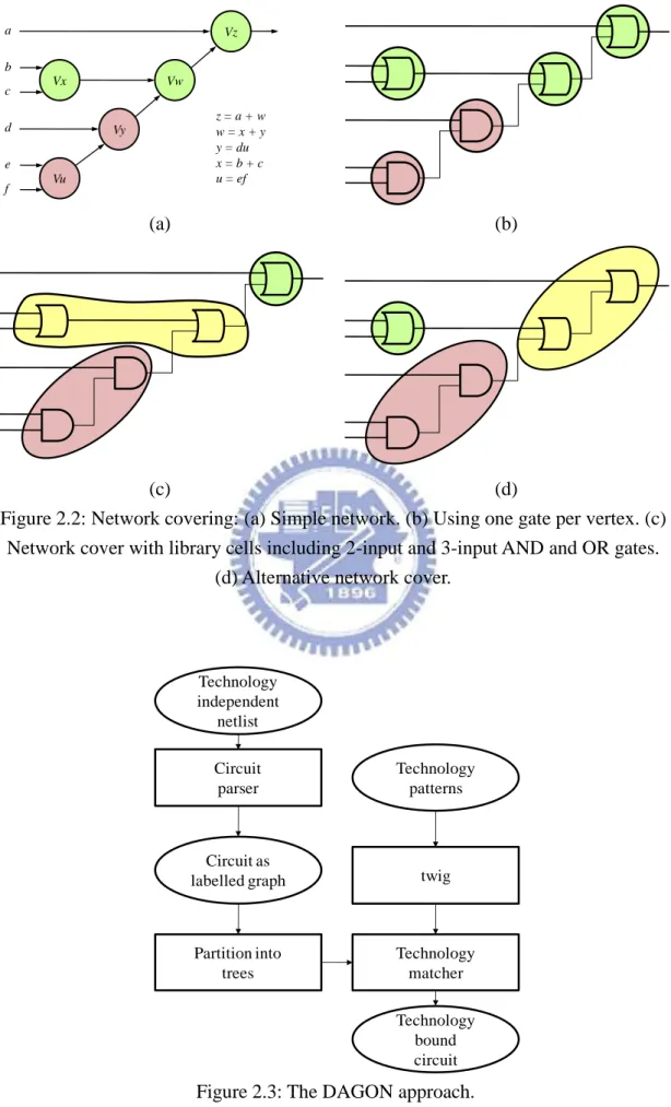
標準的 ASIC 晶片設計流程大致可分為前段與後段兩大部分。前段的主要內 容為硬體語言描寫,邏輯合成(logic synthesis)及驗證等步驟;後段則包含擺置、 繞線及之後的流程。邏輯合成將晶片設計從 RTL 層級轉換到邏輯閘層級,同時 也要驗證轉換前後的設計是否相同。邏輯合成的結果大致決定了晶片的面積、效 能,甚至決定這個設計能否達到量產的階段,過於緊湊的 slack 可能使得設計在 佈局及繞線的階段無法被實現。邏輯合成常見的做法為 network covering [2]:給 定一個 library,包含邏輯合成可使用的基本邏輯閘,在面積或是時序的條件下, 將邏輯設計以 library cells 替換,Figure 2.2。I. DAGON
Kurt [11]提出一個建立在 DAG 的方法。其演算法如 Figure 2.3 所示。首先, 電路會從 multiple fanout 的點被截成許多 subtrees。接著根據 library 內可用的 cells 建立 patterns。然後再以上一步所建立的 patterns 完成每個 subtrees,並以動態規 劃找出最小 cost 的組合。DAGON 是一個相當有效率的合成器,其複雜度為線性; DAGON 保證第一步所分割的每個 tree 都會有最佳解,但是這個方法並沒有全面 的考量電路的架構,最後的合成的結果可能受限於區域最佳化而錯失最佳解。
12
(a) (b)
(c) (d)
Figure 2.2: Network covering: (a) Simple network. (b) Using one gate per vertex. (c) Network cover with library cells including 2-input and 3-input AND and OR gates.
(d) Alternative network cover.
Figure 2.3: The DAGON approach.
Vx Vz Vw Vy Vu b c d e f a z = a + w w = x + y y = du x = b + c u = ef Technology independent netlist Circuit parser Circuit as labelled graph Partition into trees Technology patterns twig Technology matcher Technology bound circuit
13
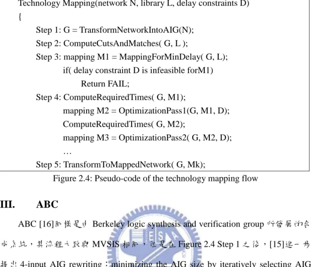
II. MVSIS
MVSIS [13][14]是由 Berkeley logic synthesis and verification group 所發展,是 一個多重目標最佳化的合成器。其主要合成步驟如 Figure 2.4。步驟一會先將電 路設計轉換成 AIG,由 2-pinput And 及 Inverter 所組成的電路,其中的每個節點 代表 2-input AND。步驟二根據 library 中所提供的 cells,計算每個節點可能的 match。接著步驟三在最小 delay 的考量下,將適合的 match 指定到節點。如果給 定的 delay 可以符合,步驟四會進一步做最佳化。來到步驟五,經過最佳化的電 路會逐一被轉換實際的電路。
另外要特別介紹的是 area recovery,這個部分會被下一段所介紹的 ABC 所 延用,同時也是這篇論文的利用的重點之一。MVSIS 結合兩個 heuristic approaches 以縮減面積。第一步,每個 node n 在不違反 required time 的前提下挑選最佳的 area flow,AF(n) = [Area(n) + i AF(Leafi(n))]/NumFanout(n)
Area(n): the area of the best match at n.
Leafi(n): the i-th leaf of the cut of the best match at n.
NumFanout(n): the number of fanouts of n.
Area flow 考慮了兩個 logic cones 重疊的程度,為 technology mapping 提供更為廣 泛的視野,避免在同一個 logic cone 來回多次。
接著,再探訪每個 node,以區域化的角度選擇最適合的 match,此時 match 是以其 maximum fanout-free cone (MFFC)內所有 gate area 總和為面積。
14
Technology Mapping(network N, library L, delay constraints D) {
Step 1: G = TransformNetworkIntoAIG(N); Step 2: ComputeCutsAndMatches( G, L );
Step 3: mapping M1 = MappingForMinDelay( G, L); if( delay constraint D is infeasible forM1)
Return FAIL; Step 4: ComputeRequiredTimes( G, M1); mapping M2 = OptimizationPass1(G, M1, D); ComputeRequiredTimes( G, M2); mapping M3 = OptimizationPass2( G, M2, D); … Step 5: TransformToMappedNetwork( G, Mk);
Figure 2.4: Pseudo-code of the technology mapping flow
III.
ABC
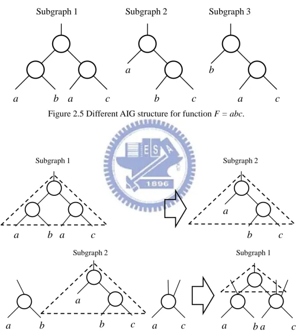
ABC [16]同樣是由 Berkeley logic synthesis and verification group 所發展的合 成系統,其流程大致與 MVSIS 相同,但是在 Figure 2.4 Step 1 之後,[15]進一步 提出 4-input AIG rewriting:minimizing the AIG size by iteratively selecting AIG subgraphs rooted at a node and replacing them with smaller pre-computed subgraphs 。 藉由移除 redundant AIG subgraph 以減少轉換成一般邏輯電路所需要的資源。首 先 ABC 會先以 topological 順序找出所有 4-input(包含以下)的 AIG subgraphs,接 著根據 subgraph root 的 function 及其 NPN-class 從 pre-computed subgraphs array 中出具有相同 function 的 subgraphs,然後從上一步找出的 subgraphs 中找出適合 的 subgraph 以減少 nodes 的數量。Figure 2.5 列出 F = abc 不同結構的 AIG subgraphs,subgraph1 有三個 nodes,subgraph2\subgraph3 都只有兩個 nodes。一 般來說,當既有的 AIG 存在 subgraph1 的情況下,會以 subgraph2/subgraph3 取代, 如 Figure 2.6 上半部所示;然而 Figure 2.6 在下半部所呈現的情形,以 subgraph1 取代 subgraph2 卻能額外減少一個 node。
15
就建立 basic subgraphs array,使得 AIG rewriting 能夠有效的降低 AIG node 的個 數,而且相當有效率。另外,ABC 在這個系統中也加入 BDD 的功能,當 library cells 中沒有 AND/NOT gate,讓電路可以被轉換成 BDD, 使得多工器可以直接 替換 BDD 中的 nodes。
Figure 2.5 Different AIG structure for function F = abc.
Figure 2.6 Two cases of AIG rewriting of a node.
a
b
c
a
b
c
a
a
c
b
Subgraph 2 Subgraph 3 Subgraph 1b
c
a
a
b
c
a
Subgraph 2 Subgraph 1a
c
a
b
b
c
a
a
b
a
c
Subgraph 1 Subgraph 216
2.1.5 DFS Algorithm
根據需要執行 ECO 的清單建立一個 DAG,從每個 PO 往 PI 尋找有連線關係 的 ECOs,並將其視為同一個群組。2.2
Problem Formulation
本篇論文所要解決的問題在於以最少的 cost 下的條件下,以預先埋入的 spare cells 完成 ECO 所需要修正的 function。標準流程的 technology mapping,所有的元件其使用數量沒有受到限制,而 且擺放的位置並未決定;然而當晶片設計來到實體設計的階段,ECO resynthesis 所能夠使用的 spare cells 卻有數量的限制,而且這些 spare cells 都有其固定的坐 標。另外需要在意的是設計上其它正常的擺置及繞線不能被破壞,因此, resynthesis 需要考慮後續繞線的複雜度。
給定一個原始的實體設計,可用的 spare cell 資訊及需要修正的 function list, 這個問題有兩點需要被考慮:
1. 如何正確的以 spare cells 所提供的 cell types 完成 ECO。
17
Chapter 3 Our Algorithm
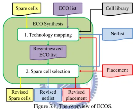
這個章節將會介紹我們在處理 ECO 所提出的演算法及複雜度分析。如章節 2.2 所介紹,Metal-only ECO 需要考慮 resynthesis 的正確性,同時要降低後續繞 線的複雜度,因此我們提出兩階段的流程來處理 ECO 的問題。Figure 3.1 描述 ECOS 的主要流程。
Figure 3.1: The overview of ECOS.
1. ECO technology mapping:根據 spare cells 所提供的 cell types 重新合成 ECO list。更詳細的介紹將會在後續的章節呈現。
2. Spare cell selection:根據第一個步驟所得到的 resynthesized ECO list,當 ECO 之間存在競爭時,考慮 spare cells 的坐標,挑選適合的 spare cells 使得繞線 的複雜度最小。
Netlist Spare cells ECO list
Placement Cell library ECO Synthesis
2. Spare cell selection Resynthesized ECO list 1. Technology mapping Revised placement Revised netlist Revised Spare cells
18
3.1
Guided ABC
Figure 3.2 詳細列出 Guided ABC 之流程。主要分為三個步驟:(a) Library cell grouping (b)ECO list partitioning (c) cell mapping。
Figure 3.2: Detailed guided ABC.
3.1.1 Library Cells Grouping
Library 中包含各式各樣的 cells,可能有相同的 function 但是名稱不相同。 為了有效的利用資源,需要根據 cell function 先行分析。因此,我們將每個 cell 轉換成 AIG,並計算 NPN-class。屬於同一個 NPN-class 的 cells 可執行相同的 function。
3.1.2 ECO List Partitioning
ECO 的需求可能來自 timing/function 的修正,或是規格的變更。前者在實際 的擺置情況可能是較為分散且細微,但是規格的變更造成的影響可能較為集中且 連續,我們對這兩種情形分開處理。Figure 3.3 為 ECO list 中可能的出現的電路, ECO1 會把 U3 換成一個 OR gate,ECO2 把 U2 換成一個 AND gate。如果 ECO1、 ECO2 彼此獨立,在 cell mapping 的階段,每個 ECO 會從其周圍挑選 cost 最小的
Technology mapping Guided ABC Cell library ECO list Library cells grouping ECO list partitioning Cell mapping Resynthesized ECO list
19
cell type:U2 會還擇 SPARE1(AND),U3 會選擇 SPARE2(OR)。如果需要修正的 電路有直接的連線關係,相關的 ECO 會一起被重新合成,最佳化目標為以最少 量的 spare cells 來實現, 因此所有的 spare cells 都會被考慮。Figure 3.3 中的 ECO list 只需要一個 spare cell SPARE3(AOI21)即可完成,不僅可以節省 spare cells 同 時可降低繞線的複雜度。
Figure 3.3: Example for ECO list partitioning.
3.1.3 Cell Mapping
ECO list partitioning 將初始的 ECO list 依據彼此的相依性被切割成多個 ECO lists。這個階段會逐一的 mapping 每個 ECO list。然而將會面對兩個問題:(1) physical information consideration,(2) equivalence checking。
我們以 COSTtype = HPBBleast-inc
反應 spare cells 的實際位置對於 resynthesis 的影響。Spare cell cost 的計算為 half-perimeter bounding box (HPBB),首先與 ECO 直接相連的所有 cells 會形成一 個 bounding box,當 spare cell 被 ECO 選用,會使得 bounding box 改變,其 half-perimeter 的最小差異即為 HPBBleast-inc。為一調整參數使得 COSTtype 的值
不超過 100。以下將以一則範例說明不同 cell type 之 cost 計算。
如 Figure 3.4(a)所示,ECO1 要求 U3 以 AND gate 替換,設計中有三個 spare cells SPARE3 SPARE2 SPARE1 out1 in1 in2 U1 U2 U3 U4 in1 in2 net1 net2 net3 out2 out1 (0, 0) (5000, 5000) out1 in1 in2 U1 U2 U4 U3 SPARE2 SPARE1 SPARE3 out2 ECO list:
ECO1: net3 = NOR(net1, net2) ECO2: net2 = AND(in1, in2)
20
可 供 使 用 。 一 開 始 與 ECO1 相 連 的 所 有 cells 所 形 成 的 bounding box 其 half-perimeter 為 6000。接著要計算每個 spare cells 的 cost,;SPARE1 座落在原 始的 bounding box 外,當 SPARE1 被 ECO1 選用時,會改變 bounding box, half-perimeter 增加 1000,cost(SPARE1) = 1000,Figure 3.4(b);而 SPARE2 位在 原始的 bounding box 內,當 SPARE2 被 ECO1 還用時,並不會增加 half-perimeter, cost(SPARE2) = 0,Figure 3.4(b)。SPARE3 同樣會使得 half-perimter 增加 1000, cost(SPARE3) = 1000。接著計算 cell types cost,SPARE1 與 SPARE2 同樣是 AND gate,我們會選最小的 cost 即 HPBBleast-inc,做為 cell types cost,因此在這個範例
中,COSTAND = 0;COSTNOT = 1000。
ECOS 內部融合既有的 synthesizer 執行 technology mapping,我們以 2.1.3 所 介紹的 ABC 做為 resynthesis 的核心,同時解決 equivalence checking 的問題。ABC 合成過程的主要考量是 delay 的限制,接著 area recovery 在不影響 delay 的前提 下嘗試以面積較小的 library cells 替換原有的 netlist。在使用上,我們將 spare cells 所提供的 cell types 改寫成 ABC 所使用的 library,library 中 cells 的 delay 被設定
為零,COSTtype會被設定成 ABC 中面積的參數,使得 area recovery 能有效的反
21 (a)
(b)
(c)
Figure 3.4: (a) Original design. (b) Bounding box including SPARE1. (c) Bounding box including SPARE2.
SPARE3 SPARE2 SPARE1 out1 in1 in2 U1 U2 U3 U4 in1 in2 net1 net2 net3 out2 out1 (0, 0) (5000, 5000) out1 in1 in2 U1 U2 U4 U3 SPARE2 SPARE1 SPARE3 out2 ECO list:
ECO1: net3 = AND(net1, net2)
SPARE3 SPARE2 SPARE1 out1 in1 in2 U1 U2 U3 U4 in1 in2 net1 net2 net3 out2 out1 (0, 0) (5000, 5000) out1 in1 in2 U1 U2 U4 U3 SPARE2 SPARE1 SPARE3 out2 SPARE3 SPARE2 SPARE1 out1 in1 in2 U1 U2 U3 U4 in1 in2 net1 net2 net3 out2 out1 (0, 0) (5000, 5000) out1 in1 in2 U1 U2 U4 U3 SPARE2 SPARE1 SPARE3 out2
22
3.1.4 Mapping Strategy
Figure 3.5: Mapping strategy.
ABC 是以 AIG 做為基本架構,因此合成時最基本需求是 AND gate 及 NOT gate,缺乏其中一種都會造成 ABC 中斷。因此 Guided ABC 需要事先檢視 cell types,當 library 中存在 AND gate 及 NOT gate,Guided ABC 會執行 general mapping;然而當 AND/NOT gate 缺乏其中一種,例如 testcase4 中的 library 沒 有 AND gate,只有 MUX 和 NOT,Guided ABC 就會建立 BDD,再以 MUX 跟 NOT 替換,如 Figure。
3.2
Spare Cell Selection: Stable Matching
guided ABC 決定修正 ECO 需要的 spare cell types 之後,在沒有競爭的情況 下,ECO resynthesis 已經完成。然而在 ECO 分佈過於靠近或是 spare cells 資源 太少的情況下,ECO 之間可能對於 spare cells 有競爭的狀況發生。雖然 guided ABC 考慮了實體資訊,卻無法處理 ECO 之間對 spare cell 的競爭。同一個 spare cell 可能同時是多個 ECO 的最佳選擇,guided ABC 會複製這個 spare cell 給多個 ECO。
Library
consists of
NOT &
AND?!
General mapping
ROBDD
construction
ECO list
Mapping with
MUX/NOT
No
Yes
23
然而實際上每個 spare cell 都是獨一無二的,當它被某一個 ECO 選定後,其它的 ECO 便無法再使用,必需另外找出具有同樣 function 的 spare cell。stable matching algorithm[17]可以解決這樣的窘境,經由 stable matching,每個 ECO 都會找到其 所需的 spare cells,同時也會是其最佳的選擇。
24
Chapter 4 Experimental Results
本篇論文之演算法以 C++程式語言實現。程式之執行環境為 2.0GHz CPU、 4GB 記憶體。
以下將呈現在 5 個 industrial testcases 執行的數據,前三個 testcases 使用一般 的 library cells 實現 ECO;最後兩個 testcases 提供的 spare cells 只有多工器及 inverter。Table 1 的左半部列出每個 testcases 的 pin 數目、cell 數目、net 數目及 spare cells 數目。原始設計的檔案是以 DEF 格式呈現,然而 ECO list 是 VERILOG 的檔案格式。Table 1 的右半部是 ECO 的數目、free-up cells 數目,並列出 Blind ABC 和 Guided ABC 所使用的 spare cells 數量。Blind ABC 沒有考慮實體資訊,僅是 將手工的方式改成自動化。相較於 Blind ABC,Guided ABC 總是能以較少的 spare cells 完成 ECO。
Table 4.1: Statistics on testcases and on ECO.
Statistics #ECOs
Case #Pin #Cell #Net #Spare #Req #FR Blind ABC Guided ABC
testcase1 483 28,591 28,705 350 7 7 16 11
testcase2 483 28,591 28,705 2,300 49 51 295 153
testcase3 483 28,591 28,705 2,300 94 121 313 162
testcase4 33 198 181 40 4 3 5 4
25
Table 2 列 出 cost 的 比 較 及 CPU time 。 經 由 Guided ABC 合 成 出 的 resyntheisized ECO list,再以 stable matching 處理競爭關係,總是能夠有效的改 善 cost。另外就 CPU time 的角度來看,我們的方法相當的有效率。
Figure 4.1 是 testcase4 的實際情況,Table 是相關資訊,有 3 個 ECO、40 個 spare cells。其中的長方形外框是 ECO 的 bounding box,藍色空心格子是 spare cells, 實心格子是被選用的 spare cells。在這個例子中,每個 ECO 都已找到其最佳解。 Figure 4.1 是 testcse3 之實際分佈,ECOs 集中在左半部,造成許多競爭關係,增 加 cost。
Table 4.2: Comparison on total cost.
Total cost
Before ECO Direct Guided ABC CPU time Ratio
testcase1 4,049,536,290 4,062,343,750 4,051,207,450 0 0.997 testcase2 4,142,631,960 4,414,703,560 4,349,716,160 1 0.985 testcase3 4,142,631,960 4,640,619,480 4,562,885,920 2 0.983
testcase4 2,310,270 2,652,430 2,323,150 0 0.876
26
27
28
Chapter 5 Conclusion
5.1 Concluding Remarks
在本篇論文中,我們就 Metal-only ECO 的問題建立了一個系統,ECOS,有 效 的 實 現 functional/timing ECO 。 有 效 地 降 低 修 改 光 罩 的 成 本 , 並 抒 解 time-to-market 的壓力。
這個系統主要分為兩個部分:第一部分為 ECO resynthesis;第二部分為 spare cell selection 。 本 篇 論文 在 第 一 個階 段 發 展出 guided ABC 。 不同 於 標 準 的 synthesizer,不需要考慮資源的限制,ECO resyntheiszer 必需利用有限的 spare cells 完成 ECO list。guided ABC 根據 spare cells 的種類、個數及實體資訊合成出 ECO list 所需要的 cells,同時避免距離太遠或是個數太少的 spare cells 被使用,有效 的降低 spare cell selection 的負擔。當競爭關係出現時,我們採用 stable matching algorithm 選出最佳的 spare cells 使得 cost 為最小。
29
Bibliography
[1] International technology roadmap for semiconductors (ITRS), 2007. http://www.itrs.net/.
[2] G. De Micheli. Synthesis and optimization of Digital Circuit. McGraw-Hill, 1994.
[3] Synopsys, Inc. http://www.synopsys.com/.
[4] Cadence Design System. http://www.cadence.com/. [5] Magma Design Automation. http://www.magma-da.com/.
[6] J.-Y. Li and Y.-L. Li. An efficient tile-based ECO router with routing graph reduction and enhanced global routing flow. In Proc. OF International Symposium on Physical Design, pages 7-13, 2005.
[7] C.-P. Lu, M. C.-T. Chao, C.-H. Lo, and C.-W. Chang. A metal-only-ECO solver for input slew and output loading violations. In Proc. OF International Symposium on Physical Design, pages 191-198, 2009.
[8] Y.-P. Chen, J.-W. Fang and Y.-W. Chang. ECO timing optimization using spare cells and technology remapping. In Proc. Of International Conference on Computer-Aided Design, pages 530-535, 2007.
[9] Y.-M. Kuo, Y.-T. Chang, S.-C. Chang and M. Marek-Sadowska. Engineering change using spare cells with constant insertion. In Proc. Of International Conference on Computer-Aided Design, pages 544-547, 2007.
[10] Y.-R. Wu, S.-Y. Chen, K.-Y. Lee, and T.-C. Wang. On Using Spare Cells for Functional Changes with Wirelength Consideration. In Proc. SASIMI, 2009. [11] K. Keuter. DAGON: Technology binding and local optimizations by DAG
matching. In Proc. of Design Automation Conference, pages 617-623, 1987. [12] SIS: A system for sequential circuit synthesis.
30
http://www.eecs.berkeley.edu/Pubs/TechRpts/1992/2010.html/.
[13] S. Chatterjee, A. Mishchenko, R. Brayton, T. Kam and X. Wang. Reducing Structural Bias in Technology Mapping. In IEEE Transaction on Computer-Aided Design, vol 26, no. 2, Dec. 2006, pages 2894-2903.
[14] MVSIS: Logic Synthesis and Verification.
http://embedded.eecs.berkeley.edu/Respep/Research/mvsis/index.html.
[15] A. Mishchenko, S. Chatterjee and R. Brayton. DAG-aware AIG rewriting a fresh look at combinational logic synthesis. In proc. of Design Automation Conference, Pages 532–535, 2006.
[16] ABC: A system for sequential synthesis and verification. http://www.eecs.berkeley.edu/~alanmi/abc/.
[17] D. Gale and L. S. Shapley. College admissions and the stability of marriage. American Mathematical Monthly, vol. 69, pages 9-14, 1962.
[18] A. Kuehlmann, V. Paruthi, F. Krohm, and M. K. Ganai. Robust boolean reasoning for equivalence checking and functional property verification. IEEE TCAD, vol. 21, no. 12, Dec. 2002, pages 1377–1394.
[19] S.B. Akers. Binary Decision Diagrams. IEEE Transactions on Computers, vol. 27, no. 6, June 1978, pages 509-516.