國 立 交 通 大 學
電子工程學系 電子研究所碩士班
碩 士 論 文
以複晶矽薄膜電晶體製作新穎高速電荷儲存式
記憶體之研究
Study on the Novel High Speed Charge
Trapping Memory Devices with Poly-Si TFTs
研 究 生:劉晏廷 Yen-Ting Liu
指導教授:鄭晃忠博士 Dr. Huang-Chung Cheng
以複晶矽薄膜電晶體製作新穎高速電荷儲存式
記憶體之研究
Study on the Novel High Speed Charge
Trapping Memory Devices with Poly-Si TFTs
研 究 生:劉晏廷 Student: Yen-Ting Liu
指導教授:鄭晃忠博士 Advisor: Dr. Huang-Chung Cheng
國立交通大學
電子工程學系 電子研究所碩士班
碩士論文
A Thesis
Submitted to Department of Electronics Engineering
& Institute of Electronics
College of Electrical & Computer Engineering
National Chiao Tung University
In Partial Fulfillment of the Requirements
for the degree of master
in
Electronics Engineering
2010
Hsinchu, Taiwan, Republic of China
i
以複晶矽薄膜電晶體製作新穎高速電荷儲存式記憶體
之研究
研究生:劉晏廷 指導教授:鄭晃忠 博士
國立交通大學
電子工程學系 電子研究所碩士班
摘要
由於傳統的電荷儲存式記憶體在寫入和抹除的速度上,比起懸浮閘極式記憶 體有一段差距,因此,近年來許多人致力於進行改善電荷儲存式記憶體寫入和抹 除速度的研究。然而,大多數能改善寫入和抹除速度的方法,同時也造成了一些 可靠度不佳的問題。在這篇論文,我們分成兩個主題進行研究。第一個,在 SONOS 之電荷儲存式記憶體架構上,以 FinFET、Omega Gate 與 GAA 之結構探討其角隅效應。利用角隅這種尖銳的幾何結構能提升在穿隧層 的電場並降低在阻擋層的電場,進而大大地加快寫入速度。因此,以 GAA 結構 設計的 SONOS 記憶體展現出最高的寫入效率,也進一步證明了有越多角隅的 SONOS 記憶體擁有越快的寫入效率。
ii
第二個,在 SONOS 之架構上,以真空取代穿隧氧化層,並以高介電常數介
電質作為阻擋層,設計成新穎的 TANVAS 和 THNVAS 記憶體元件。採用 Al2O3 或
HfO2 作為阻擋層,或使用真空作為穿隧層,皆能增加在穿隧層的電場並降低在
阻擋層的電場,進而促使寫入和抹除速度能顯著的提升。因此,TANVAS 和 THNVAS 比起 TANOS 和 THNOS 有較高的寫入和抹除效率。對使用 oxide 作為 穿隧層的記憶體元件來說,在經過幾個寫入/抹除週期後,oxide 穿隧層很容易受 到外力的傷害而產生缺陷,使用真空作為穿隧層則能克服這項問題,所以 TANVAS 記憶體元件展現出良好的元件耐久度特性。在電荷保存能力方面,由於
oxide 穿隧層中的 traps 和 HfO2阻擋層的低能障高度皆有助於載子的流動,容易
形成漏電路徑,因此 THNVAS 和 TANOS 無法長時間將載子保存於電荷儲存層 內。TANVAS 避開了這些問題,所以展現出良好的資料保存性。
在經過對電性的探討和分析後,我們得到一些令人滿意的結果。我們的研究 能顯著地提升寫入和抹除的速度,同時還能維持良好的元件耐久度和資料保存性。 這在未來的高密度電路和系統面板具有相當大的發展潛力。
iii
Study on the Novel High Speed Charge Trapping
Memory Devices with Poly-Si TFTs
Student: Yen-Ting Liu Advisor: Dr. Huang-Chung Cheng
Department of Electronics Engineering & Institute of Electronics
National Chiao Tung University
ABSTRACT
In recent years, many researchers have drawn attention to improve the program/erase efficiency of charge trapping memory devices owing to the program/erase efficiency of conventional charge trapping memory devices is lower than that of floating gate memory devices. However, most methods of improving the program/erase efficiency resulted in poor reliability issues. In this thesis, our investigation has been classified into two topics.
At first, for Poly-Si TFT SONOS memory devices, we have proposed a FinFET structure, an omega gate structure, and a GAA structure to investigate the corner effect. Since the sharp corner geometric will increase electric field in the tunneling layer and decrease electric field in the blocking layer, the program speed can be enhanced greatly. Consequently, the SONOS memory device with a GAA structure
iv
exhibits the highest program efficiency and it proves that SONOS memory devices with more corners will enhance program efficiency.
On the other hand, we have proposed novel high speed Poly-Si TFT TANVAS and THNVAS memory devices with high-k blocking layer and vacuum tunneling layer. Utilizing high-k materials, such as Al2O3 and HfO2, as blocking layer or using
low-k materials, like vacuum, as tunneling layer can increase electric field in the tunneling layer and decrease electric field in the blocking layer. Based on this field enhanced scheme, the proposed memory devices reveal excellent memory performance. It is shown obviously that the TANVAS and THNVAS memory devices have higher program/erase efficiency than the TANOS and THNOS memory devices. Furthermore, the conventional SiO2 tunneling layer is always suffered from damage
after program/erase cycles. Using vacuum tunneling layer can overcome this obstacle so that the TANVAS memory device exhibits better endurance characteristics. Due to the traps in oxide tunneling layer and lower conduction band offset in HfO2 blocking
layer will provide leakage paths for charges, the TANOS and THNVAS memory devices are not able to preserve stored charges for a long time. The TANVAS memory device can avoid these problems and presents great retention characteristics.
Through investigating and analyzing the electrical characteristics, we obtain some satisfying results. The program/erase efficiency of proposed memory device is enhanced remarkably, and exhibits great endurance and retention characteristics. They are very promising for future applications in high density circuits and SOP.
v
誌謝
非常感謝指導教授鄭晃忠博士在我碩士班這兩年對我的諄諄教誨,讓我無論 在知識學習或做人處世上都有顯著的成長。 也非常感謝俊諭學長在實驗和研究上對我的指導,在我遇到問題時總是無怨 無悔的和我討論,幫助我突破難關,順利完成研究。 感謝大傳學長、明華學長、聖凱學長、邦祐學長和伯鈞學弟在實驗和生活上 的幫忙,沒有你們的協助,可能很多時候我會忙不過來。 最後我要感謝父母的養育之恩,無論我遇到什麼困難,總是在背後支持著我, 讓我總是能從挫折中站起來,邁開步伐大步向前行。vi
Contents
Abstract (in Chinese)………...i
Abstract (in English)……….iii
Acknowledgements ………...v
Contents……….……vi
Table Lists…...………viii
Figure Captions……….ix
Chapter 1 - Introduction
1-1. Overview of the Low Temperature Poly-crystalline Silicon Thin-Film Transistors……….……….11-2. Introduction of the SONOS Nonvolatile Memory Devices………...……….2
1-2-1. Floating Gate and SONOS Non-volatile Memory Devices………...2
1-2-2. Program/Erase Mechanisms of SONOS Non-volatile Memory Devices………...4
1-2-3. Reliability of SONOS Non-volatile Memory Devices…...7
1-3. Motivation………...………8
1-4. Thesis Organization………....9
Chapter 2 - Corner Effect of Poly-Si TFT SONOS Memory Devices
with FinFET, Omega Gate, and Gate-All-Around structures
2-1. Introduction……….………..112-2. Device Fabrication of Poly-Si TFT SONOS with FinFET, Omega Gate, and Gate-All-Around structures………….……….12
vii
2-4. Results and Discussion……….16
2-4-1. Simulation Result…...16
2-4-2. Program efficiencies of the three structures………...17
2-4-3. Subthreshold swing shifts of the three structures...18
2-5. Summary………...………19
Chapter 3 - Poly-Si TFT TANVAS and THNVAS Memory Devices
with a FinFET Structure
3-1. Introduction………...………203-2. Device Fabrication of Poly-Si TFT TANVAS and THNVAS with a FinFET structure………...….22
3-3. Materials Analysis………...……….23
3-4. Results and Discussion……….24
3-4-1. Read Disturbance………25
3-4-2. Program/Erase Efficiencies of FinFET TANOS and CP TANOS...25
3-4-3. Program/Erase Efficiencies of FinFET TANVAS and FinFET TANOS...26
3-4-4. Program/Erase Efficiencies of FinFET THNVAS and FinFET THNOS……...28
3-4-5. Endurance Characteristics of TANVAS, TANOS, and THNVAS…...30
3-4-6. Retention Characteristics of TANVAS, TANOS, and THNVAS...32
3-5. Summary………...………33
Chapter 4 - Summary and Conclusions
………...………34References
………...36viii
Table Lists
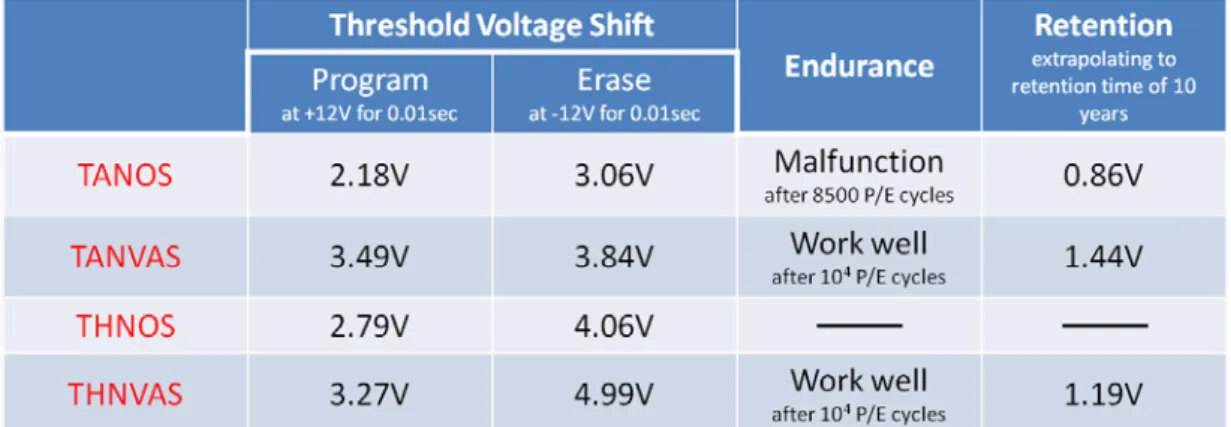
Table 3-1 The electrical characteristics of the FinFET TANOS, TANVAS, THNOS, and THNVAS memory devices………..………..42
ix
Figure Captions
Chapter 1
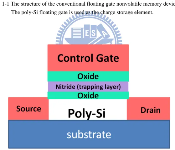
Fig. 1-1 The structure of the conventional floating gate nonvolatile memory device. The poly-Si floating gate is used as the charge storage element………43
Fig. 1-2 The structure of the SONOS nonvolatile memory device. The nitride layer is used as the charge-trapping element………..43
Fig. 1-3 Proposed trajectory of an emitted channel electron. An energetic electron is redirected toward the interface by an acoustic phonon scattering…………..44
Fig. 1-4 (a) Direct tunneling is associated with transversal of a trapezoidal barrier. (b) Fowler-Nordheim Tunneling is associated with transversal of a triangular barrier………...44
Fig. 1-5 Illustration of Band to band tunneling. (a) Electron-hole pairs appear in the deep-depletion region layer in the n+ drain. (b) The path of electron-hole pair in energy band diagram………..45
Fig. 1-6 Band diagram of trapped charges loss path in SONOS: trap-to-band tunneling (T-B), trap-to-trap tunneling (T-T), band-to-trap tunneling (B-T), thermal excitation (TE) and Frenkel-Poole emission (PF)……….45
Chapter 2
Fig. 2-1 The cross-section view step of the strip formation for the FinFET structure.46
Fig. 2-2 The cross-section view step of the a-Si spacers formation for the FinFET structure………..46
Fig. 2-3 The cross-section view step of the nanowire-channel formation for the FinFET structure………....47
x
Fig. 2-4 The cross-section view step of the gate formation for the FinFET structure.47
Fig. 2-5 The cross-section view step of the strip formation for the omega gate
structure and the GAA structure……….48
Fig. 2-6 The cross-section view step of the a-Si spacers formation for the omega gate structure………..48
Fig. 2-7 The cross-section view step of the nanowire-channel formation for the omega gate structure………...49
Fig. 2-8 The cross-section view step of the gate formation for the omega gate
structure………..49
Fig. 2-9 The cross-section view step of the nanowire-channel formation for the GAA structure………50
Fig. 2-10 The cross-section view step of the gate formation for the GAA structure...50
Fig. 2-11 The cross-section TEM image after patterning gate for the omega gate structure………51
Fig. 2-12 The magnifying cross-section TEM image after patterning gate for the omega gate structure……….51
Fig. 2-13 The distribution of electrical field across the stacked ONO dielectrics for the
omega gate structure at VGS = 18 V………..52
Fig. 2-14 The distribution of electrical field across the stacked ONO dielectrics for the
GAA structure at VGS = 18 V………...52
Fig. 2-15 The distribution of electrical field across the stacked ONO dielectrics for the first corner in the omega gate structure at VGS = 18 V……….53
Fig. 2-16 The distribution of electrical field across the stacked ONO dielectrics for the second corner in the omega gate structure at VGS = 18 V………53
xi
Fig. 2-17 The transfer characteristics of the FinFET structure memory device with
various programming times at VGS= 18 V………...54
Fig. 2-18 The transfer characteristics of the omega gate structure memory device with
various programming times at VGS= 18 V………...54
Fig. 2-19 The transfer characteristics of the GAA structure memory device with
various programming times at VGS= 18 V………...55
Fig. 2-20 The comparison of threshold voltage shifts between the FinFET structure, the omega gate structure, and the GAA structure memory devices after programming operation………55
Fig. 2-21 The comparison of subthreshold swing shifts between the SONOS memory devices with a FinFET structure, an omega gate structure, and a GAA structure………56
Chapter 3
Fig. 3-1 The cross-section view step of the gate formation before etching oxide for the TANVAS memory device………..57
Fig. 3-2 The cross-section view step of the gate formation after etching oxide for the TANVAS memory device………..57
Fig.3-3 The cross-section schematic image after patterning gate and ion
implantation………...…….58
Fig.3-4 The cross-section schematic image after nitride spacers formed………58
Fig. 3-5 The cross-section schematic image after etching tunneling oxide with 1:10 diluted BOE………59
Fig. 3-6 The cross-section schematic image after depositing passivation oxide……..59
xii
Fig. 3-8 The tiled view SEM image of multiple nanowire channels for the TANVAS memory device………...60
Fig. 3-9 The top view SEM image for the TANVAS memory device……….61
Fig. 3-10 The designed mask patterns for the TANVAS memory device…………...61
Fig. 3-11 The magnifying tiled-view SEM image for the TANVAS memory device.62
Fig. 3-12 The transfer characteristics of TANVAS memory device when the program
bias is set as VGS= 6 V………..62
Fig. 3-13 The transfer characteristics of the FinFET TANOS device with various
programming times at VGS= 12 V………63
Fig. 3-14 The transfer characteristics of the FinFET TANOS device with various
erasing times at VGS= -12 V……….63
Fig. 3-15 The transfer characteristics of the CP TANOS device with various
programming times at VGS= 12 V………64
Fig. 3-16 The transfer characteristics of the CP TANOS device with various erasing
times at VGS= -12 V………..64
Fig. 3-17 The comparisons of threshold voltage shifts between the FinFET TANOS device and the CP TANOS device after program operation………65
Fig. 3-18 The comparisons of threshold voltage shifts between the FinFET TANOS device and the CP TANOS device after erase operation………..65
Fig. 3-19 The transfer characteristics of the FinFET TANVAS device with various
programming times at VGS= 12 V………66
Fig. 3-20 The transfer characteristics of the FinFET TANVAS device with various
erasing times at VGS= -12 V……….66
Fig. 3-21 The comparisons of threshold voltage shifts between the FinFET TANVAS device and the FinFET TANOS device after program operation………….67
xiii
Fig. 3-22 The comparisons of threshold voltage shifts between the FinFET TANVAS device and the FinFET TANOS device after erasing operation…………...67
Fig. 3-23 The comparisons of threshold voltage shifts of the FinFET TANVAS device between various program biases………...68
Fig. 3-24 The comparisons of threshold voltage shifts of the FinFET TANVAS device between various erase biases………68
Fig. 3-25 The comparisons of threshold voltage shifts of the FinFET TANOS device between various program biases………...69
Fig. 3-26 The comparisons of threshold voltage shifts of the FinFET TANOS device between various erase biases………69
Fig. 3-27 The transfer characteristics of the FinFET THNVAS device with various
programming times at VGS= 12 V………70
Fig. 3-28 The transfer characteristics of the FinFET THNVAS device with various
erasing times at VGS= -12 V……….70
Fig. 3-29 The transfer characteristics of the FinFET THNOS device with various
programming times at VGS= 12 V………71
Fig. 3-30 The transfer characteristics of the FinFET THNOS device with various
erasing times at VGS= -12 V……….71
Fig. 3-31 The comparisons of threshold voltage shifts between the FinFET THNVAS device and the FinFET THNOS device after program operation………….72
Fig. 3-32 The comparisons of threshold voltage shifts between the FinFET THNVAS device and the FinFET THNOS device after erase operation………..72
Fig. 3-33 The comparisons of threshold voltage shifts between the FinFET TANVAS device and the FinFET THNVAS device after program operation………..73
Fig. 3-34 The comparisons of threshold voltage shifts between the FinFET TANVAS device and the FinFET THNVAS device after erase operation…………...73
xiv
Fig. 3-35 The transfer characteristics of the FinFET TANVAS device with various
programming times at VGS= 9 V………..74
Fig. 3-36 The transfer characteristics of the FinFET TANVAS device with various erasing times at VGS= -9 V………...74
Fig. 3-37 The threshold voltage shifts of the FinFET TANVAS device with various programming/erasing times after programming and erasing operation…...75
Fig. 3-38 The endurance characteristics of FinFET TANVAS device………75
Fig. 3-39 The endurance characteristics of FinFET TANOS device………...76
Fig. 3-40 The endurance characteristics of FinFET THNVAS device………76
Fig. 3-41 The retention characteristics of FinFET TANVAS device………...77
Fig. 3-42 The retention characteristics of FinFET TANOS device……….77
Fig. 3-43 The comparison of the retention characteristics between FinFET TANVAS device and FinFET TANOS device………..78
Fig. 3-44 The retention characteristics of FinFET THNVAS device………...78
Fig. 3-45 The comparison of the retention characteristics between FinFET TANVAS device and FinFET THNVAS device………...79
1
Chapter 1
Introduction
1-1. Overview of the Low Temperature
Poly-crystalline Silicon Thin-Film Transistors
Many researchers have made much focus on low temperature poly-crystalline silicon thin film transistors (LTPS TFTs) in recent years due to the applications of LTPS TFTs in active matrix liquid crystal displays (AMLCDs) [1] and active matrix organic light emitting displays (AMOLCDs) [2]. The advantages of LTPS TFTs, such as higher field-effect mobility and better compatibility with different substrates, are the reasons why LTPS TFTs have been increasingly used in active matrix displays.
Hydrogenated amorphous silicon thin film transistors (a-Si:H TFTs) were introduced at the beginning of the AMLCD industry. Amorphous silicon TFTs exhibit low leakage current owing to the high off-state resistivity. Furthermore, they are compatible with large-area glass substrate for low processing temperature. Nevertheless, the low field-effect mobility (typically less than 1 cm2/V-s) of a-Si:H TFTs is not adequate to drive peripheral circuits.
Thanks to the field-effect mobility of LTPS TFTs is normally higher than that of a-Si:H TFTs by two orders of magnitude, the peripheral circuits can be driven with sufficiently high currents in LTPS TFTs [3]. Therefore, the pixel arrays and the peripheral circuits can be integrated on the same substrate [4]-[6], even on a single
2
panel, which is an advanced technology called system on panel (SOP) [7]. Meanwhile, LTPS TFTs have potential to be applied in three-dimension integrated circuits (3-D ICs) [8].
1-2. Introduction of the SONOS Nonvolatile
Memory Devices
1-2-1. Floating Gate and SONOS Non-volatile Memory Devices
Non-volatile memory devices are widely used for data storage in modern electronic systems. Recently, non-volatile flash memory devices have become the mainstream in the semiconductor memory industry due to the mass data storage requirements in electronic products. There are two different types of non-volatile flash memory devices which are famous in the world, that is, floating gate (FG) and charge trapping non-volatile flash memory devices.
The major difference between floating gate and charge trapping non-volatile flash memory devices is the material of the charge storage layer. The floating gate devices (shown in Fig. 1-1) utilize poly-Si film as charge storage layer and charge trapping devices take nitride film as it. One of the typical charge trapping devices is known as silicon-oxide-nitride-oxide-silicon (SONOS) memory device (shown in Fig. 1-2).
Since the floating gate is made of conducting material, the stored charges are capable of flowing freely inside the floating gate without any restriction. It means,
3
even if electrons only can jump to charge storage layer by flowing through a specific position of tunneling layer, electrons can keep flowing and flowing from channel into charge storage layer until the charge storage layer is full of electrons and has no more position to save any charge. As a result, floating gate memory devices have great program/erase speed.
However, there are some concerns regarding the capability to scale down the tunneling dielectric thickness [9]. If the tunneling oxide is not thick enough, the stored charges in the floating gate might leak out and lose easily through the defects which are inside the tunneling oxide. After many program/erase cycles, there will be more and more defects inside the tunneling oxide [10]. These kinds of stress induce leakage current (SILC) phenomena lead to poor reliability characteristics.
On the contrary, the charge storage layer of SONOS memory devices, the nitride film, stores charges into the discrete deep-level traps. The stored charges in the nitride film will not leak out so easily jsut like those in the floating gate [11]. The SONOS memory devices improve the phenomenon of SILC and show the better reliability characteristics.
In addition, the floating gate memory devices have the issue of gate coupling between adjacent cells. The interference between adjacent cells will change the electrical characteristics of floating gate memory devices, and cause memory devices lack stability and uniformity. Moreover, it will raise the difficulty to scale down the whole devices. In contrast, the SONOS memory devices avoid the issue of gate coupling. As a consequence, they have great ability to scale down and enhance the electrical characteristics vitally.
4
1-2-2. Program/Erase Mechanisms of SONOS Non-volatile
Memory Devices
Program and erase speed are the crucial factors to estimate performance of SONOS Non-volatile memory devices. Nowadays, there are three main program/erase mechanisms. The three program/erase mechanisms are channel hot electron injection (CHEI), Fowler-Nordheim tunneling (FN tunneling) and band to band tunneling (BTBT).
Channel Hot Electron Injection
When drain voltage (Vds) is larger than saturation drain voltage (Vds,sat), a
pinch-off region will occur near the drain side in the channel and there will be a high lateral electric field inside the pinch-off region. When electrons flows from source to drain, they will be accelerated and gain much energy in the pinch-off region. Some electrons have high enough energy are called “hot electrons” (shown in Fig. 1-3). At the same time, gate bias provides vertical electric field to help those hot carriers inject into charge trapping region. Then, some hot electrons will overcome the barrier of conduction band, inject into charge trapping region, and store in there. It is known as “lucky-electron model” [12].
Due to the effective mass of holes is heavier than that of electrons, and the barrier height of the valence band is higher than that of the conduction band, it is really hard for holes to overcome the barrier and inject into the charge trapping region.
5
It follows that hot-hole injection is rarely employed in non-volatile memory operation.
Fowler-Nordheim Tunneling
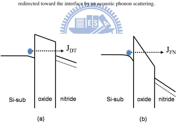
According to the strength of electric field across the tunneling oxide and the thickness of tunneling oxide, the tunneling mechanism can be classified into two different types, direct tunneling and Fowler-Nordheim (FN) tunneling (shown in Fig. 1-4).
(1) Direct tunneling:
If the electric field strength across the tunneling oxide (Eox) is smaller than
𝑞𝜙𝑜𝑥
𝑡𝑜𝑥 , where 𝜙𝑜𝑥 is the barrier height of conduction band between tunneling oxide
and silicon channel, the carriers will tunnel into charge trapping layer by direct tunneling.
The formula of direct tunneling is expressed as:
𝐽 ∝ 𝑒
−𝛼𝑡𝑜𝑥where
𝛼 =
2�2𝑞𝑚𝜙𝑜𝑥ℏ
(2) Fowler-Nordheim tunneling:
If the electric field strength across the tunneling oxide (Eox) is larger than 𝑞𝜙𝑜𝑥
𝑡𝑜𝑥 ,
6
[14].
The formula of Fowler-Nordheim tunneling is expressed as:
𝐽 = 𝐴𝐸
𝑜𝑥2𝑒
− 𝐵𝐸𝑜𝑥 where𝐴 =
𝑞 2 16𝜋2ℏ𝜙𝑜𝑥 and𝐵 =
4√2𝑚(𝑞𝜙𝑜𝑥 )32 3ℏ𝑞Band to Band Tunneling
If a negative gate voltage and a positive drain voltage are provided for a N-type SONOS memory device, and the strength of electric field across the junction is high enough to form a deep-depletion region, then band to band tunneling will occur in the overlap region of gate and drain, and electron hole pairs will be generated by band to band tunneling (shown in Fig. 1-5).
In the mean time, electrons will tunnel across the energy band gap from valence band to conduction band at the drain region. Holes will be generated in the deep-depletion region and then will be attracted by the negative gate bias to tunnel into the charge trapping layer. By the phenomenon of tunneling of holes into the charge trapping layer, band to band tunneling is a new method which is used for erasing in some SONOS memory devices [15].
7
1-2-3. Reliability of SONOS Non-volatile Memory Devices
Retention
Ideally, the amount of storage charges in the charge storage layer would remain in a fixed value after the procedure of program or ease, but it is impossible in the real life. In fact, the stored charges would keep losing and losing until the electrical characteristics of the whole SONOS memory device achieve a steady balance [16] [17]. Therefore, retention is a critical measurement to realize the relationship between charge loss and time, and to estimate whether a SONOS non-volatile memory device could retain sufficient charges in the charge trapping layer.
There are three major mechanisms of charge loss which is pertinent to time, one is thermal excitation (TE), another is Frenkel-Poole emission (FP), and the other one is tunneling through tunneling oxide (shown in Fig. 1-6). The stored electrons in charge trapping layer would tunnel back to the conduction band of the silicon substrate by trap-to-band tunneling (T-B), or to the interface traps between tunneling oxide and silicon channel by trap-to-trap tunneling (T-T). Furthermore, holes from the valence band of the silicon substrate would tunnel into the traps in the charge trapping layer by band-to-trap tunneling (B-T).
8
After numerous cycles of programming and erasing, some charges will be trapped in the tunneling oxide by external stress and high electric field, and the defects will result in the raise of leakage current and degrade the quality of tunneling oxide [18]. If there are more and more trapped charges and defects in the tunneling oxide, the SONOS memory devices will break down and malfunction very easily. As a result, endurance is an essential measurement to assist us to evaluate if SONOS memory devices are capable of tolerating the damage of external stress, working normally and maintaining great electrical characteristics after many cycles of programming and erasing [19].
1-3. Motivation
Poly-crystalline silicon thin film transistors (Poly-Si TFTs) have attracted much attention because of their prosperous applications in active matrix displays [20]-[23], and potential for development in system on panel (SOP) and three-dimension integrated circuits (3-D ICs). Recently, Poly-Si TFTs are prevalent to be employed for data storage, especially for non-volatile flash memory devices [24]. In addition, Poly-Si TFT SONOS memory devices become more promising than Poly-Si TFT floating-gate memory devices since the Poly-Si TFT SONOS memory devices have better capability to scale down and better compatibility with CMOS process.
In order to improve and upgrade the electrical characteristics of Poly-Si TFT SONOS memory devices, we propose some novel SONOS memory devices and discuss some effects and phenomena in the thesis. It will be classified into two distinct topics. It is well-known that multiple-gate structures exhibit superior
9
gate-control ability and enhance the performance of SONOS memory devices [29]-[32]. However, a few of researches are studied for finding out the crucial factors in improving the performance of SONOS memory devices. The first topic is to discuss the corner effect of SONOS memory devices, and we tried to fabricate three kinds of Poly-Si TFT SONOS memory devices with a FinFET structure, an omega gate structure, and a GAA structure to make sure the relationship between the corner and the performance of SONOS memory devices.
Using High-k material as blocking layer is a very popular method of improving program/erase speed nowadays [37]-[39]. In the second topic, we present two novel high speed charge trapping memory devices, TiN-Al2O3-Nitride-Vacuum-Silicon
(TANVAS) and TiN-HfO2-Nitride-Vacuum-Silicon (THNVAS), which combine
high-k blocking layer (Al2O3 and HfO2) with low-k tunneling layer (vacuum). From
an electrostatics consideration, the use of vacuum tunneling layer will cause a larger voltage drop across the tunneling layer and smaller voltage drop across high-k blocking layer. As compared to the TiN-Al2O3-Nitride-Oxide-Silicon (TANOS) and
TiN-HfO2-Nitride-Oxide-Silicon (THNOS) memory devices, the proposed structures
have the advantage of high program/erase speed as well as the good charge-retention time. Therefore, such TANVAS and THNVAS memories are very promising for the future applications in high density circuits and SOP.
1-4. Thesis Organization
In chapter 1, there are concise introductions of low temperature poly-crystalline silicon thin film transistors (LTPS TFTs) and SONOS non-volatile flash memory
10
devices. Subsequently, the motivations of the thesis are explored to introduce the thesis.
In chapter 2, the fabrication processes of SONOS memory devices with various corners are described. The most important components of device structures are analyzed by transmission electron microscope (TEM). Moreover, the electrical characteristics are investigated and reviewed.
In chapter 3, the fabrication processes of TANVAS memory devices with high-k blocking layer, metal gate, and vacuum tunneling layer are described. The most important components of device structures are analyzed by scanning electron microscope (SEM) and transmission electron microscope (TEM). Furthermore, the electrical characteristics of TANVAS memory devices are discussed in detail.
11
Chapter 2
Corner Effect of Poly-Si TFT SONOS
Memory Devices with FinFET, Omega
Gate, and Gate-All-Around structures
2-1. Introduction
In recent years, a MOSFET with a multiple gates structure is a very popular research subject. Many different kinds of multiple gates structures have been proposed in present semiconductor industry, such as double gates [25], triple gates [26], FinFET [27] and gate-all-around (GAA) [28]. Multiple gates structures exhibit superior gate control ability and high electrical performance [29]-[32]. Meanwhile, the short channel effects can be suppressed efficiently as well. Multiple gates structures are also applied to non-volatile flash memory devices nowadays. They are employed to enhance programming/erasing efficiency and to scale down the memory devices [33]-[36].
For multiple gates structures, the electrical characteristics are varied in different positions of channel. For example, the electrical characteristics in corner and in planar parts are totally dissimilar. We fabricated three distinct SONOS memory devices with three types of multiple gates structures, those are, a FinFET structure with one corner, an omega gate structure with two corners, and a GAA structure with three corners. In this chapter, we will investigate corner effect of those memory devices and find out
12
the relationship between corners and device performance characteristics.
2-2. Device Fabrication of Poly-Si TFT SONOS
with
FinFET, Omega Gate, and Gate-All-Around
structures
We fabricated three kinds of poly-crystalline silicon thin film transistor Silicon-Oxide-Nitride-Oxide-Silicon (Poly-Si TFT SONOS) memory devices with a FinFET structure, an omega gate structure, and a GAA structure, respectively. The fabrication processes are listed below.
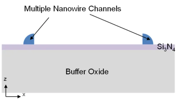
Poly-Si TFT SONOS with a FinFET structure
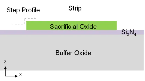
At first, a 1000-nm-thick wet-oxide was thermally grown on 6-inch silicon wafers. Then, a 50-nm-thick Si3N4 film was deposited on wet-oxide by low pressure
chemical vapor deposition (LPCVD) system at 780 °C as an etch-stop layer and a 100-nm-thick tetra-ethyl-ortho-silicate (TEOS) SiO2 film was deposited on etch-stop
nitride by LPCVD system at 700 °C to be a sacrificial layer. It was patterned with a lithography step and the TEOS SiO2 film was etched by reactive ion etch (RIE) to
form several strips with step height of 100-nm (shown in Fig. 2-1). Subsequently, a 100-nm-thick amorphous silicon film was deposited by LPCVD system at 560 °C.
13
After that, it was patterned with a source/drain-pad mask, the amorphous silicon film was etched by RIE to form amorphous silicon spacers, and the amorphous silicon spacers were connected to the source/drain pads which were formed to be the device active region (shown in Fig. 2-2). Next, a solid phase crystallization (SPC) at 600 °C in N2 ambient for 24 hours was performed to transform amorphous silicon into
poly-crystalline silicon.
FinFET structure was formed after etching the 100-nm-thick TEOS SiO2 strips
with 3:50 diluted HF (shown in Fig. 2-3), and the etch-stop layer would stop the 3:50 diluted HF etching the buried oxide. Then, a 6.5-nm-thick TEOS SiO2 film, a
10-nm-thick Si3N4 film, a 12.5-nm-thick TEOS SiO2 film, and a 200-nm-thick
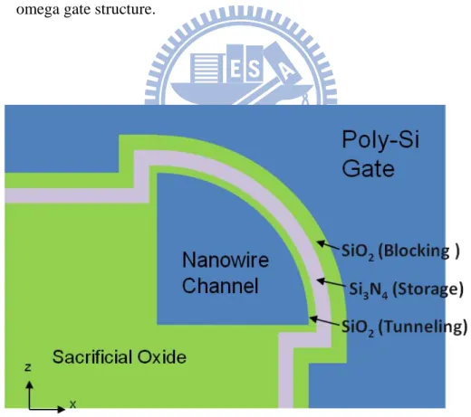
phosphorous in-situ doped poly-Si film were deposited sequentially by LPCVD to be the tunneling layer, the charge trapping layer, the blocking layer and the gate, accordingly (shown in Fig. 2-4).
Following the gate patterning, the poly gate, SiO2 blocking layer, Si3N4 trapping
layer and SiO2 tunneling layer were etched by RIE. Then, a phosphorous ion
implantation was performed with the dosage of 5×1015 cm-2 and the energy of 30 keV. Next, a 350-nm-thick passivation oxide was deposited by LPCVD system and then the source/drain activation at 950 °C in N2 ambient for 30 seconds was performed.
Afterward, contact holes were patterned and the passivation oxide was etched by 1:15 diluted BOE. A 500-nm-thick Al film was deposited by FSE - cluster - PVD subsequently. Finally, metal electrodes were patterned and then the Al metal film was etched to complete the fabrication.
14
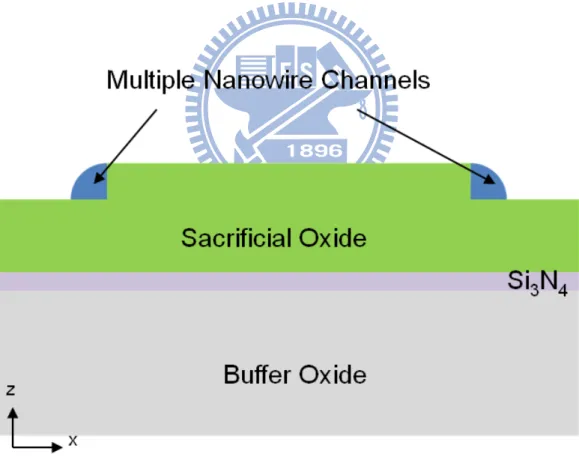
For the Poly-Si TFT SONOS memory devices with an omega gate structure (shown in Fig. 2-8) and a GAA structure (shown in Fig. 2-10) formation, we will only list different fabrication processes below.
A 300-nm-thick tetra-ethyl-ortho-silicate (TEOS) SiO2 film was deposited on
etch-stop nitride by LPCVD system at 700 °C to be a sacrificial layer. It was patterned with a lithography step and the TEOS SiO2 film was etched by reactive ion
etch (RIE) to form several strips with step height of 100-nm (shown in Fig. 2-5). Subsequently, a 100-nm-thick amorphous silicon film was deposited by LPCVD system at 560 °C. After that, it was patterned with a source/drain-pad mask, and the amorphous silicon film was etched by RIE to form amorphous silicon spacers. The amorphous silicon spacers were connected to the source/drain pads which were formed to be the device active region (shown in Fig. 2-6). Next, the solid phase crystallization (SPC) at 600 °C in N2 ambient for 24 hours was performed to
transform amorphous silicon into poly-crystalline silicon. An omega gate structure was formed after etching the TEOS SiO2 film with 3:50 diluted HF in a specific time
(shown in Fig. 2-7).
Poly-Si TFT SONOS with a GAA structure
A 300-nm-thick tetra-ethyl-ortho-silicate (TEOS) SiO2 film was deposited on
etch-stop nitride by LPCVD system at 700 °C to be a sacrificial layer. It was patterned with a lithography step and the TEOS SiO2 film was etched by reactive ion
15
etch (RIE) to form several strips with step height of 100-nm. Subsequently, a 100-nm-thick amorphous silicon film was deposited by LPCVD system at 560 °C. After that, it was patterned with a source/drain-pad mask, the amorphous silicon film was etched by RIE to form amorphous silicon spacers, and the amorphous silicon spacers were connected to the source/drain pads which were formed to be the device active region. Next, the solid phase crystallization (SPC) at 600 °C in N2 ambient for
24 hours was performed to transform amorphous silicon into poly-crystalline silicon. A GAA structure was formed after etching the 300-nm-thick TEOS SiO2 film with
3:50 diluted HF, and the etch-stop layer would stop the 3:50 diluted HF etching the buried oxide (shown in Fig. 2-9).
2-3. Materials Analysis
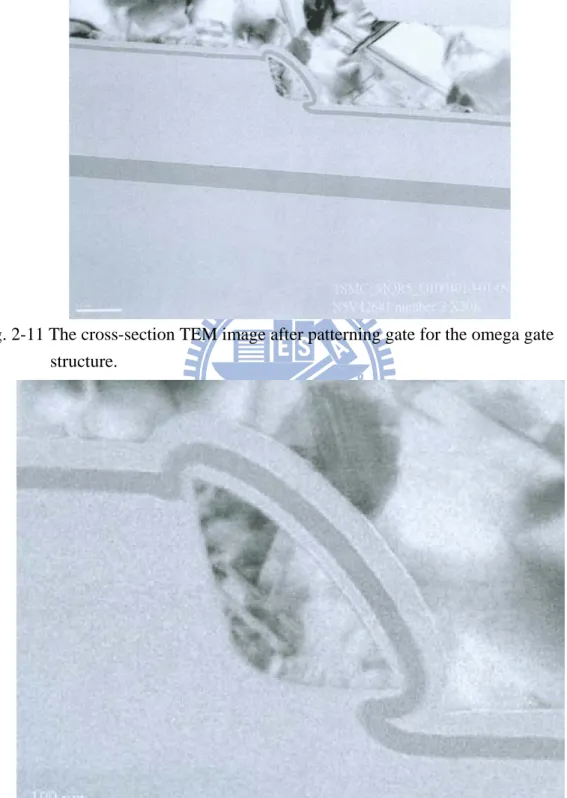
After fabricating SONOS memory devices, materials analysis is essential to check if the finished products accord with the original designs. In this section, transmission electron microscope (TEM) is used to analyze the key fabrication processes and structures of the SONOS memory devices.
Figure 2-11 and figure 2-12 show the cross-section TEM images of the omega gate structure. It is obvious that the omega gate structure is in accordance with the original design by controlling precisely the wet-etching time. In addition, from the TEM images, we can make sure the thicknesses of the oxide tunneling layer, the nitride trapping layer, and the oxide blocking layer are 6.5 nm, 10 nm, and 12.5 nm, respectively.
16
2-4. Results and Discussion
We fabricated three kinds of poly-crystalline silicon thin film transistor Silicon-Oxide-Nitride-Oxide-Silicon (Poly-Si TFT SONOS) memory devices with a FinFET structure, an omega gate structure, and a GAA structure, respectively. The corner effect of those three structures is discussed from the device simulation, program efficiency, and the subthreshold swing shift.
2-4-1. Simulation Result
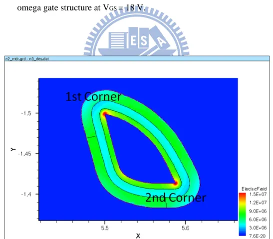
In order to demonstrate the electric field distribution of the omega gate structure and the GAA structure, a numerical simulation was carried using ISE-TCAD. Figure 2-13 and figure 2-14 show the electric field distribution of those two structures at a gate bias of 18 V. It is observed that electric field of tunneling layer in the corner is higher than that in the planar part, and electric field of blocking layer in the corner is lower than that in the planar part. Due to fabrication always has some discrepancy, the shape of the structures are not standard quarter circles. Therefore, the radius of curvature for each corner is not the same. Figure 2-15 and figure 2-16 show the distribution of electric field across the ONO stack for the two corners in the GAA structure. Since the first corner is sharper than second corner, the first corner exhibits higher electric field in the tunneling layer and lower electric field in the blocking layer. It proves that sharp geometric structures make electric field concentrate on tunneling layer.
17
2-4-2. Program efficiencies of the three structures
The Fowler-Nordheim (FN) tunneling mechanism is employed in this thesis for the FinFET structure, the omega gate structure, and the GAA structure. Figure 2-17, figure 2-18, and figure 2-19 show the transfer characteristics of the FinFET structure, the omega gate structure, and the GAA structure memory devices with various programming times at VGS= 18 V, respectively. Figure 2-20 shows the comparison of
threshold voltage shifts between those memory devices after programming operation. The FinFET structure SONOS memory device exhibits a Vth shift of 1.57 V in 10 ms,
the omega gate structure exhibits a Vth shift of 2.98 V and the GAA structure exhibits
a Vth shift of 3.52 V. It is obvious that the GAA structure device has highest program
efficiency, the omega gate structure device comes second, and the FinFET structure device is the third.
According to the simulation results, it is quite clear that the electric field across the tunneling layer can be enhanced owing to the sharp corner geometry. Higher electric field in the tunneling layer increases the probability of carriers injecting into the charge trapping layer, and lower electric field in the blocking layer suppresses the back tunneling effect. Therefore, the program efficiency would be enhanced greatly. A GAA structure has most corners and that is the reason why the SONOS memory device with a GAA structure exhibits highest program efficiency.
18
2-4-3. Subthreshold swing shifts of the three structures
In our experiments, subthreshold swing would alter owing to two possible reasons, local charge effect and interface states.
At first, since the program speed in the corner region is faster than that in the planar part, the amount of nitride trapped charges in the corner are more than that in the planar part in a specific programming time. The electrical characteristics in the corner and in the planar part will be different, and that is called local charge effect. More nitride trapped charges in the corner would raise the subthreshold swing shift. Therefore, we can realize program efficiency by observing subthreshold swing shift. Figure 2-21 shows the comparison of subthreshold swing shifts between the SONOS memory devices with a FinFET structure, an omega gate structure, and a GAA structure. The subthreshold swing shift of the SONOS memory device with a GAA structure is the largest, the shift of the SONOS memory device with an omega gate structure comes second, and the shift of the SONOS memory device with a FinFET structure is the least. The largest subthreshold swing shift means most charges inject into nitride trapping layer in the corners. Therefore, the SONOS memory device with a GAA structure has the most charges injection in the nitride trapping layer, and it exhibits the highest program efficiency at the same programming time.
On the other hand, we have already known that electric field of tunneling layer in the corner is higher than that in the planar part. Higher electric field in the tunneling layer increases the probability of carriers injecting into the charge trapping layer, but also increases the probability of damaging the channel/dielectric interface at the same time. More dangling bonds and interface traps will raise the subthreshold swing shift. Therefore, the SONOS memory device with a GAA structure seems to have the most
19
dangling bonds and interface traps, and exhibits the largest subthreshold swing shift.
2-5. Summary
We have demonstrated three kinds of poly-crystalline silicon thin film transistor Silicon-Oxide-Nitride-Oxide-Silicon (Poly-Si TFT SONOS) memory devices with a FinFET structure, an omega gate structure, and a GAA structure, respectively. From simulation results, the sharp geometry of corner enhances the electric field at the Si/tunneling oxide interface and depresses the electric field in the blocking oxide. Higher electric field in the tunneling layer and lower electric field in the blocking layer enhance the program speed greatly. Moreover, a GAA structure has most corners. Consequently, the SONOS memory device with a GAA structure exhibits highest program efficiency.
20
Chapter 3
Poly-Si TFT TANVAS and THNVAS
Memory Devices with a FinFET
Structure
3-1. Introduction
Oxide is the most typical material which is applied to tunneling layer and blocking layer of the conventional SONOS memory devices. However, the performance of the conventional SONOS memory devices is considered to be not good enough. In recent years, many researchers put much effort in studying some prominent methods to enhance the performance of SONOS memory devices. One of the prominent methods is to exploit high-k material to replace oxide as blocking layer [37]-[39].
If high-k material is used as blocking layer, voltage drop in the blocking layer would become lower and that in the tunneling layer would become higher. Likewise, electric field would concentrate on tunneling region [40]. The higher electric field would increase the speed of programming and erasing at the same time. In addition, lower electric field in the blocking layer would hinder the flow of carriers either from gate to nitride or from nitride to gate. Back tunneling effect would be reduced [41][42], then SONOS memory devices would exhibit better performance and larger window.
21
Higher electric field improves the speed of programming and erasing, but it will result in some charges trapped easily in the tunneling oxide and degrade the quality of tunneling oxide [43]-[44]. Then, the phenomenon of stress induces leakage current (SILC) will become more obvious. In terms of retention, more defects in tunneling oxide make more leakage paths exist, and the stored charges will flow across the tunneling layer very easily even no external force is exerted on the memory device. It will present a bad consequence in retention. For endurance, trapped charges will be accumulated in the tunneling oxide after program/erase cycles, and it will lead to the threshold voltages of programmed and erased states move upward more rapidly. If the threshold voltage shift is too large, the memory devices will break down in a short period. Therefore, higher electric field has the chance to diminish the life time of memory devices, and reveal unfavorable effects in endurance.
In order to ameliorate the reliability characteristics, we propose a novel poly-crystalline silicon thin film transistor TiN-Al2O3-Nitride-Vacuum-Silicon
(Poly-Si TFT TANVAS) memory device structure which the tunneling oxide is replaced with vacuum. It is difficult for charges to be trapped in the vacuum tunneling layer, so the leakage current and the defects will be suppressed at the same time. It follows that the TANVAS memory device will exhibit better reliability characteristics of retention and endurance. Furthermore, vacuum is a low-k material, and utilizing low-k material as tunneling layer also has the effect of increasing the voltage drop and electric field in the tunneling layer. It means that vacuum tunneling layer is capable of enhancing the efficiency of programming and erasing.
22
3-2. Device Fabrication of Poly-Si TFT TANVAS and
THNVAS with a FinFET structure
We fabricated novel poly-crystalline silicon thin film transistor
TiN-Al2O3-Nitride-Vacuum-Silicon (Poly-Si TFT TANVAS) and
TiN-HfO2-Nitride-Vacuum-Silicon (Poly-Si TFT THNVAS) memory devices with a
FinFET structure and the fabrication processes will be listed below.
At first, a 1000-nm-thick wet-oxide was thermally grown on 6-inch silicon wafers. Then, a 50-nm-thick Si3N4 film was deposited on wet-oxide by low pressure
chemical vapor deposition (LPCVD) system at 780 °C as an etch-stop layer and a 100-nm-thick tetra-ethyl-ortho-silicate (TEOS) SiO2 film was deposited on etch-stop
nitride by LPCVD system at 700 °C to be a sacrificial layer. It was patterned with a lithography step and the TEOS SiO2 film was etched by reactive ion etch (RIE) to
form several strips with step height of 100-nm. Subsequently, a 100-nm-thick amorphous silicon film was deposited by LPCVD system at 560 °C. After that, it was patterned with a source/drain-pad mask, the amorphous silicon film was etched by RIE to form amorphous silicon spacers, and the amorphous silicon spacers were connected to the source/drain pads which were formed to be the device active region. Next, a solid phase crystallization (SPC) at 600 °C in N2 ambient for 24 hours was
performed to transform amorphous silicon into poly-crystalline silicon.
FinFET structure was formed after etching the 100-nm-thick TEOS SiO2 strips
with 3:50 diluted HF, and the etch-stop layer would stop the 3:50 diluted HF etching the buried oxide. Then, a 4-nm-thick TEOS SiO2 film and a 10-nm-thick Si3N4 film
were deposited sequentially by LPCVD to be the tunneling layer and the charge trapping layer, respectively. Afterward, a 10-nm-thick Al2O3 film (or HfO2 film) was
23
deposited by metal organic chemical vapor deposition (MOCVD) system at 550 °C to be the blocking layer. Behind the deposition of the ANO stack, a 300-nm-thick TiN film was deposited by FSE - cluster - physical vapor deposition (PVD) to be the metal gate (shown in Fig. 3-1).
Following the gate patterning, the TiN gate, Al2O3 blocking layer and Si3N4
trapping layer were etched by RIE, but the 4-nm-thick TEOS SiO2 film was still
remained on the wafer. Then, a phosphorous ion implantation was performed with a dosage of 5×1015 cm-2 and an energy of 40 keV. Afterwards, a 300-nm-thick Si3N4
was deposited and it was etched back by RIE to form Si3N4 spacers. Because the
Si3N4 spacers wrapped around the Al2O3 blocking layer, they were capable of
preventing Al2O3 blocking layer from being etched by the following wet-etching. The
tunneling oxide was side-etched for 500-nm with 1:10 diluted BOE to form a vacuum tunneling layer (shown in Fig. 3-2 ~ Fig. 3-6).
Next, a 400-nm-thick passivation oxide was deposited by SiH4-based PECVD
system and then the source/drain activation at 950 °C in N2 ambient for 30 seconds
was performed. Afterward, contact holes were patterned and the passivation oxide was etched by 1:10 diluted BOE. A 500-nm-thick Al film was deposited by FSE - cluster - PVD subsequently. Finally, metal electrodes were patterned and then the Al metal film was etched to complete the fabrication.
3-3. Materials Analysis
After fabricating TANVAS memory devices, materials analysis is essential to check if the finished products accord with the original designs. In this section,
24
scanning electron microscope (SEM) is used to analyze the key fabrication processes and structures of the TANVAS memory devices.
Figure 3-7 and figure 3-8 show the tiled-view SEM images of the TANVAS memory device. Gate, source, drain, and multiple nanowire channels are shown clearly in the SEM images. Figure 3-9 shows the top-view SEM image and figure 3-10 shows the designed mask patterns of the TANVAS memory device. In order to etch all the deposited oxide in the tunneling layer to form a vacuum tunneling layer and ensure the entire device would not collapse after etching, we designed a jagged gate pattern. From the top-view SEM image and the image of designed mask patterns, we can see the jagged gate is completely the same as our design. Figure 3-11 shows the magnifying tiled-view SEM images of the TANVAS memory device. The vacuum tunneling layer on the nanowire channel is shown distinctly in the magnifying SEM image.
3-4. Results and Discussion
In this section, the memory performances of two novel poly-crystalline silicon thin film transistor, TiN-Al2O3-Nitride-Vacuum-Silicon (Poly-Si TFT TANVAS) and
TiN-HfO2-Nitride-Vacuum-Silicon (Poly-Si TFT THNVAS), with a FinFET structure
are discussed. The crucial part of the research subject is to combine a high-k blocking layer with a vacuum tunneling layer for a new charge trapping memory device structure.
25
3-4-1. Read Disturbance
In order to measure the correct threshold shift of programming and erasing, it is necessary to make sure the measurement will not be interfered by other external elements. One of the typical interference is that the gate bias is too large during the ID-VG measurement, which will cause additional charges injection across the
tunneling oxide. Therefore, we need to find out the suitable bias condition of read measurement. Figure 3-12 shows the transfer characteristics of TANVAS memory device when the program bias is set at VGS= 6 V. The transfer characteristics are
almost equal within 10-2 second. It proves that read disturbance could be neglected while the gate bias of ID-VG measurement is smaller than 6 V.
3-4-2. Program/Erase Efficiencies of FinFET TANOS and CP
TANOS
For all the memory operations in this chapter, no matter TANOS, TANVAS or THNVAS, they are programmed and erased by Fowler-Nordheim (FN) tunneling mechanism.
Continuing the discussion from chapter 2, the corner effect of TiN-Al2O3-Nitride-Oxide-Silicon (TANOS) memory devices are discussed first. We
fabricated the FinFET TANOS device with one corner and the conventional planar (CP) TANOS device with no corner. Figure 3-13 and figure 3-14 show the transfer characteristics of the FinFET TANOS device with various programming/erasing times
26
at VGS= 12 V and VGS= -12 V, respectively. Figure 3-15 and figure 3-16 show the
transfer characteristics of the CP TANOS device with various programming/erasing times at VGS= 12 V and VGS= -12 V, accordingly. It is obvious that both the
programming and erasing efficiency of the FinFET TANOS device are much better than the CP TANOS device. Figure 3-17 and figure 3-18 display the comparisons of threshold voltage shifts between the FinFET TANOS device and the CP TANOS device after programming and erasing operation correspondingly. In the programming characteristics, the FinFET TANOS device exhibits a large Vth shift of 2.18 V in 10
ms at a gate pulse of 12 V, while the Vth shift of CP TANOS device is only 1.27 V. In
the erasing characteristics, the FinFET TANOS device exhibits a Vth shift of 3.06 V in
10 ms at a gate pulse of -12 V, and the Vth shift of CP TANOS device is 2.82 V It
certifies that TANOS memory devices with more corners will enhance the programming and erasing efficiency, and the corner effects in charge trapping memory devices will enlarge the memory window no matter the usage of blocking layer material.
3-4-3. Program/Erase Efficiencies of FinFET TANVAS and
FinFET TANOS
We fabricated a novel FinFET TANVAS (one corner) memory device using vacuum tunneling layer. Figure 3-19 and figure 3-20 present the transfer characteristics of the FinFET TANVAS device with various programming/erasing times at VGS= 12 V and VGS= -12 V, respectively. Figure 3-21 and figure 3-22 present
27
the FinFET TANOS device after programming and erasing operation, accordingly. In the programming characteristics, the FinFET TANVAS device exhibits a large Vth
shift of 3.49 V in 10 ms at a gate pulse of 12 V, while the Vth shift of FinFET TANOS
device is only 2.18 V. In the erasing characteristics, the FinFET TANVAS device exhibits a Vth shift of 3.84 V in 10 ms at a gate pulse of -12 V, the Vth shift of FinFET
TANOS device is 3.06 V. It is obvious that both the programming and erasing efficiency of the FinFET TANVAS device are much better than the FinFET TANOS device. The improvement on programming and erasing efficiency can be attributed to the utilization of vacuum tunneling layer. Vacuum is a low-k material, and utilizing low-k material as tunneling layer would further increase the voltage drop and electric field in the tunneling layer. In addition, voltage drop and electric field would be decreased in the blocking layer and thereby suppress the electron back tunneling effect. Consequently, the programming and the erasing speed would be increased effectively. These results verify that using vacuum tunneling layer is capable of enhancing the efficiency of programming and erasing.
Figure 3-23 and figure 3-24 show the comparisons of threshold voltage shifts of the FinFET TANVAS device with various programming/erasing biases. Figure 3-25 and figure 3-26 show the comparisons of threshold voltage shifts of the FinFET TANOS device with various programming/erasing biases. It is observed that the FinFET TANVAS device always exhibits better programming and erasing efficiency than the FinFET TANOS device even in different programming/erasing bias conditions.
Figure 3-35 and figure 3-36 show the transfer characteristics of the FinFET TANVAS device with various programming/erasing times at VGS= 9 V and VGS= -9
V, respectively. Figure 3-37 shows the threshold voltage shifts of the FinFET TANVAS device with various programming/erasing times after programming and
28
erasing operation. In the programming characteristics, the FinFET TANVAS device exhibits a Vth shift of 2.02 V in 10 ms at a gate pulse of 9 V. In the erasing
characteristics, the FinFET TANVAS device exhibits a Vth shift of 2.09 V in 10 ms at
a gate pulse of -9 V. Even if the programming and erasing biases are only 9 V, the FinFET TANVAS device is still capable of injecting charges across the tunneling layer and producing a 2-V window of threshold voltage shift in 10 ms. It proves that the FinFET TANVAS device which combines high-k blocking layer with vacuum tunneling layer can work well in low voltage operations, and this kind of low power consumption device is very promising in memory industry.
3-4-4. Program/Erase Efficiencies of FinFET THNVAS and
FinFET THNOS
We fabricated a FinFET THNVAS memory device and replaced blocking oxide with HfO2. Figure 3-27 and figure 3-28 show the transfer characteristics of the
FinFET THNVAS device with various programming/erasing times at VGS= 12 V and
VGS= -12 V, accordingly. Figure 3-29 and figure 3-30 show the transfer
characteristics of the FinFET THNOS device with various programming/erasing times at VGS= 12 V and VGS= -12 V, correspondingly. Figure 3-31 and figure 3-32 show the
comparisons of threshold voltage shifts between the FinFET THNVAS device and the FinFET THNOS device after programming and erasing operation, respectively. In the programming characteristics, the FinFET THNVAS device exhibits a large Vth shift
of 3.27 V in 10 ms at a gate pulse of 12 V, while the Vth shift of FinFET THNOS
29
exhibits a Vth shift of 4.99 V in 10 ms at a gate pulse of -12 V, and the Vth shift of
FinFET THNOS device is 4.06 V. It is obvious that both the programming and erasing efficiency of the FinFET THNVAS device is much better than the FinFET THNOS device. The improvement on programming and erasing efficiency can also be attributed to the utilization of vacuum tunneling layer. No matter the high-k blocking layer is Al2O3 or HfO2; the vacuum tunneling layers are capable of enhancing the
efficiency of programming and erasing.
Figure 3-33 and figure 3-34 show the comparisons of threshold voltage shifts between the FinFET TANVAS device and the FinFET THNVAS device after programming and erasing operation, accordingly. In the programming characteristics, the FinFET THNVAS device exhibits larger Vth shifts than the FinFET TANVAS
device before 1 ms programming time. On the contrary, the FinFET THNVAS device presents smaller memory window than the FinFET TANVAS device after 1 ms programming time. The reason why the FinFET THNVAS device exhibits larger windows before 1 ms is that the dielectric constant (k) of HfO2 is larger than that of
Al2O3. Utilizing a higher dielectric constant material as a blocking layer will
enormously increase the electric field in the tunneling layer and thereby enhance the probability of carrier injection across the tunneling layer. Therefore, the FinFET THNVAS device has faster programming speed and it exhibits larger windows of Vth
shifts before 1 ms programming time. When the dielectric constant of materials becomes higher, the energy band gap will become smaller. Due to the lower conduction band level of HfO2, the nitride storage charges will easily tunnel across
the HfO2 layer. Charges inject across tunneling layer from channel and charges inject
across blocking layer from nitride layer will reach a dynamic balance in a shorter period. Consequently, the curve of threshold voltage shifts of the FinFET THNVAS device will achieve saturation more rapidly than that of the FinFET TANVAS device
30
Therefore, the FinFET THNVAS device exhibits smaller windows of Vth shifts after 1
ms programming time. In the erasing characteristics, the FinFET THNVAS device exhibits a Vth shift of 4.99 V in 10 ms at a gate pulse of -12 V, and the Vth shift of
FinFET TANVAS device is 3.84 V. It is obvious that the erasing efficiency of the FinFET THNVAS device is much better than the FinFET TANVAS device.
3-4-5. Endurance Characteristics of TANVAS, TANOS, and
THNVAS
For memory devices, there should be a reference voltage to distinguish between programming state and erasing state. Differential sense amplifiers will determine the state by judging the relationship between threshold voltage and reference voltage. In N-channel devices, if the threshold voltage is higher than the reference voltage, differential sense amplifiers will determine it’s a programming state. On the contrary, if the threshold voltage is lower than the reference voltage, differential sense amplifiers will determine it’s an erasing state. For fresh memory devices, the reference voltage can be set as the intermediate value between threshold voltages of programming and erasing states, and it will be much easier for differential sense amplifiers to determine the state.
In the endurance measurement, if the threshold voltage of programming state is lower than reference voltage, or the threshold voltage of erasing state is higher than reference voltage, differential sense amplifiers cannot determine the correct states and memory devices will malfunction. Therefore, memory devices which can work well after much more programming/erasing cycles have better endurance characteristics.
31
Figure 3-38 and figure 3-39 show the endurance characteristics of FinFET TANVAS device and FinFET TANOS device, respectively. The memory window is 3.12 V in the fresh FinFET TANVAS device and it keeps a 2.7-V window after 104 P/E cycles. In the FinFET TANOS device, the initial memory window is 2.96 V and it keeps a 2.38-V window after 104P/E cycles. The FinFET TANVAS device has less window loss and maintains the memory window well after 104P/E cycles. There will be a higher chance for the FinFET TANVAS device to endure external stress for a long time.
According to the endurance measurements of FinFET TANVAS device and FinFET TANOS device, the curves of threshold voltages go upward gradually. It is worth to mention that the memory devices will lose function when the threshold voltage of erasing state transcends the reference voltage. There are two reasons to explain why the curves of threshold voltages would go upward gradually. The first reason is the stored charges in deep-level traps of nitride trapping layer are hard to be erased. The second reason is that the charges which are trapped in the tunneling layer and the poly-Si/SiO2 interface by external stress, thus degrading the performances of
memory devices. Those trapped charges would make the curves go upward more rapidly, and memory devices would malfunction after cycles. For the FinFET TANVAS device, it still works well after 104 P/E cycles. However, differential sense amplifiers in the FinFET TANOS device cannot determine the state after 8500 P/E cycles. It indicates that FinFET TANVAS devices have better endurance characteristics than FinFET TANOS devices. During P/E cycles, less dangling bonds and trapped charges are generated in the vacuum tunneling layer, so the FinFET TANVAS device can work well for a long time and have better endurance characteristics.
32
The memory window is 4.43 V in the fresh FinFET THNVAS device and it keeps a 3.85-V window after 104P/E cycles. The window loss of the FinFET THNVAS device is just little so that the memory window is maintained very well after 104P/E cycles. In addition, just like the FinFET TANVAS device, the FinFET THNVAS device still works well after 104 P/E cycles. It proves that charge trapping memory devices with vacuum tunneling layer can improve endurance characteristics efficiently.
3-4-6. Retention Characteristics of TANVAS, TANOS, and
THNVAS
Figure 3-41 and figure 3-42 show the retention characteristics of FinFET TANVAS device and FinFET TANOS device, accordingly. Figure 3-43 shows the comparison of the retention characteristics between FinFET TANVAS device and FinFET TANOS device. The memory window of the FinFET TANVAS device is 1.44 V after extrapolating to retention time of 10 years. The memory window of the FinFET TANOS device is only 0.86 V after extrapolating to retention time of 10 years. Due to the more traps and defects in oxide tunneling layer, it is much easier for charges to flow across tunneling layer by these traps and defects. Therefore, FinFET TANVAS devices have larger retention windows and better retention characteristics. Figure 3-44 shows the retention characteristics of FinFET THNVAS device. Figure 3-45 shows the comparison of the retention characteristics between FinFET TANVAS device and FinFET THNVAS device. The memory window of the FinFET THNVAS device is 1.19 V after extrapolating to retention time of 10 years. Although
33
the FinFET THNVAS device has a larger initial window, it has a smaller 10-year retention window than that of FinFET TANVAS device. This is because HfO2
blocking layer has smaller energy band gap. The conduction band level of HfO2 is
lower than that of Al2O3. It is much easier for charges to flow across HfO2 blocking
layer than to flow across Al2O3 blocking layer. As a result, FinFET THNVAS devices
have smaller 10-year retention windows as compared with FinFET TANVAS devices.
3-5. Summary
We have demonstrated Poly-Si TFT TANVAS, TANOS, THNVAS, and THNOS memory devices (The electrical characteristics are shown in Table 3-1). Utilizing high-k materials, such as Al2O3 and HfO2, as blocking layer or using low-k materials,
like vacuum, as tunneling layer can increase electric field in the tunneling layer and decrease electric field in the blocking layer. Therefore, program/erase efficiency would be enhanced remarkably. For TANOS and THNOS, SiO2/Si interface and SiO2
tunneling layer are liable to be damaged after some program/erase cycles. Using vacuum as tunneling layer can overcome this obstacle and exhibit better endurance characteristics. Traps in oxide tunneling layer and lower barrier of HfO2 blocking
layer would provide leakage paths for charges. As a result, the TANVAS memory devices are able to preserve stored charges for a long time and present great retention characteristics.
34
Chapter 4
Summary and Conclusions
In this thesis, we have dedicated to explore and investigate some new methods of promoting electrical characteristics for charge trapping memory devices. It has been classified into two topics. First, the corner effect of SONOS memory devices, and second, charge trapping memory devices with high-k blocking layer and vacuum tunneling layer.
In order to discuss corner effect of SONOS memory devices, we have fabricated three kinds of Poly-Si TFT SONOS memory devices with a FinFET structure, an omega gate structure, and a GAA structure. Due to the sharp corner geometry, the local electric field of channel/tunneling oxide interface can be enhanced greatly and thereby improve the program efficiency. Additionally, the electric field in the blocking oxide is deservedly diminished accompanying the suppression of electron back-tunneling. The Poly-Si TFT SONOS memory devices with a FinFET structure, an omega gate structure and a GAA structure exhibit a threshold voltage shift of 1.58V, 2.98 V and 3.52 V for FN programming at VGS = +18V in 10 ms. The SONOS
memory device with a GAA structure exhibits the highest program speed and it proves that SONOS memory devices with more corners will enhance program efficiency.
We have proposed Poly-Si TFT TANVAS, TANOS, THNVAS, and THNOS memory devices. Utilizing high-k materials, such as Al2O3 and HfO2, as blocking