Pseudo-Clock Controlled Load-dependent Frequency
Wei-Chung Chen, Student Member, IEEE, Da-Long Ming, Yi-Ping Su, Yu-Huei Lee, and
Ke-Horng Chen, Senior Member, IEEE
Abstract—A high efficiency 3.3 V-to-1 V switched-capacitor (SC)
step-down DC-DC converter with load-dependent frequency con-trol (LFC) and deep-green mode (DGM) operation is proposed for system-on-a-chip (SoC) application. According to output loading current, the LFC technique can immediately and dynamically ad-just the switching frequency through the use of pseudo-clock gen-erator (PCG) and lead-lag detector (LLD) circuit to obtain high power conversion efficiency and small output voltage ripple over a wide loading current range. Therefore, adequate loading cur-rent supplying function and output voltage regulation can be guar-anteed. Moreover, the DGM operation, similar to pulse skipping mode, can mask the switching clock to reduce power loss at ultra-light loads for further improving power efficiency. The test chip fabricated in 55 nm CMOS process demonstrates that the pro-posed fast transient converter can deliver wide load range from 10 mA to 250 mA with two small flying capacitors (
F) and one output capacitor ( F). The peak conversion efficiency is 89% compared to the ideal value of 91% . In other words, the peak normalized efficiency is equal to 98%. The overall normalized efficiency is always kept higher than 90% while the output voltage ripple is guaranteed smaller than 30 mV.
Index Terms—Deep-green mode (DGM), lead-lag detector
(LLD), load-dependent frequency control (LFC), pseudo-clock generator (PCG), switched-capacitor (SC), system-on-a-chip (SoC).
I. INTRODUCTION
I
N RECENT years, power management units are widely used in portable devices such as smart phones, notebooks, PDAs, cameras, etc. The characteristic of high power conver-sion efficiency and fully integration in system-on-chip (SoC) for a compact size is the main design goal in power management module. To provide the supply current over a wide load range, the inductor-based switching DC-DC converter is commonly used in SoC applications [1]. However, due to large occupation of print-circuit-board (PCB) area and high cost resulted from the usage of inductor, it is hard to further reduce the size of power management module especially for SoC system applica-tions. Furthermore, electromagnetic interference (EMI), which is easily derived when using the magnetic components, often becomes the thorny issue in the SoC applications.SC DC-DC converter has the features of small size, simple control scheme, and the moderate power conversion efficiency Manuscript received March 18, 2013; revised May 30, 2013; accepted August 10, 2013. Date of publication October 28, 2013; date of current version February 21, 2014. This paper was recommended by Associate Editor S. Chattopadhyay. The authors are with the Institute of Electrical Control Engineering, National Chiao Tung University, Hsinchu 30010, Taiwan.
Color versions of one or more of the figures in this paper are available online at http://ieeexplore.ieee.org.
Digital Object Identifier 10.1109/TCSI.2013.2284182
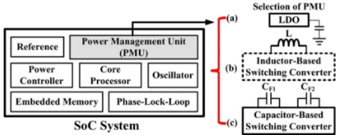
Fig. 1. Illustration of the power management in SoC applications.
[2]–[6]. Fig. 1 shows the SoC application with power man-agement unit. Owing to the advantages of small size and low cost in SC DC-DC converter, the capacitor-based switching converter is a good candidate of power management compared to the inductor-based power management. Both step-down and step-up operations can be realized through the combination of different energy delivery paths along with the distinct connec-tions of the flying capacitors [7]–[9]. In addition, to achieve the supply function in SoC applications, the closed-loop operation of the SC DC-DC converter must be activated to derive a well-regulated output voltage [10], [11]. To replace conventional inductor-based switching regulator by the SC converter, the driving capability and power conversion effi-ciency are important design issues because the power supplies are necessary to provide the SoC over a wide load range. Many control schemes have been provided to improve the overall efficiency of DC-DC converters [12]–[16]. However, prior arts are realized with large inductors or flying capacitors.
Furthermore, fully integrated SC converter with on-chip flying and output capacitors, which can be the replacement of low-dropout (LDO) regulator in some applications, has limited load current range within several mili-amperes [17]. Besides, on-chip capacitance suffers from serious parasitic capacitances and limited silicon area since the cost for the on-chip capac-itance is very high in advanced process. Moreover, if small flying capacitors and output capacitor are used, the operating frequency should be increased to ensure the driving capability. In other words, the disadvantages of on-chip capacitance are large switching loss and low flexibility.
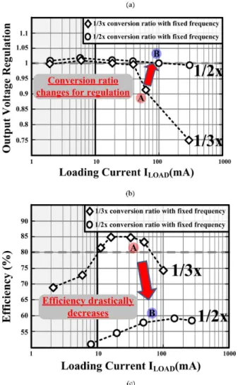
For the designs fabricated in nanometer advanced process, it’s necessary to provide core devices a regulated 1V supply voltage [17], [18]. If the input voltage ranges from 3.3 V–3.6 V and the output voltage is 1 V, the conversion ratio can be de-signed as 1/2x or 1/3x without considering any no-ideal loss. Conventional SC DC-DC architecture is shown in Fig. 2(a) to drive wide loading current range with small flying capacitors at a fixed switching frequency [19]. As illustrated in Fig. 2(b), the output voltage almost looses the regulation at the point A 1549-8328 © 2013 IEEE. Personal use is permitted, but republication/redistribution requires IEEE permission.
Fig. 2. (a) Conversional SC architecture. (b) Output voltage regulation vs. loading current. (c) Efficiency vs. loading current.
because of the insufficient current driving capability at heavy loads if 1/3x conversion ratio is utilized. To achieve high cur-rent driving capability and to regulate the output voltage, the controller can change the conversion ratio from 1/3x to 1/2x. That is, the operation point is moved from point A to point B. Although the output voltage remains regulated at heavy loads, the power efficiency will be largely reduced to an unacceptable value because 1/2x conversion ratio suffers much extra power loss compared to the 1/3x operation as illustrated in Fig. 2(c).
Consequently, one alternative way is to increase the switching frequency in the proposed design for supplying large output power and maintaining output regulation. As illustrated in Fig.
Fig. 3. Design target of power conversion efficiency in (a) and the output voltage ripple in (b) of the proposed SC DC-DC converter.
3(a), the lower switching frequencies used in SC DC-DC con-verter contributes lower power loss and thus benefits higher power conversion efficiency. However, energy supplementation is limited by low switching frequencies. That is to say, load range is restricted because of insufficient energy to output at heavy loads. In contrast, the output voltage ripple will be re-duced by increasing the frequency as shown in Fig. 3(b) and the output regulation can be guaranteed. Therefore, the load-de-pendent frequency control (LFC) technique with the deep-green mode (DGM) operation are realized in the proposed SC DC-DC converter to derive an adequate power conversion efficiency and obtain a satisfactory output voltage ripple over a wide load range. According to specific load condition, the proposed LFC technique, which contains pseudo-clock generator (PCG) and lead-lag detector (LLD) circuit, can modulate the switching fre-quency to obtain an optimum energy supply distribution. Fur-thermore, the LFC technique can gradually adjust the switching frequency in order to avoid large drop in power conversion ef-ficiency.
In order to further improve efficiency at ultra-light loads, the DGM operation takes over the operation by deeply reducing the switching frequency at the sacrifice of the output ripple. By monitoring the output energy, the controller is activated to transfer energy to the output once it requires energy and conse-quently reduces power loss. In other words, the controller stays at idle stage for saving energy and the trade-off between effi-ciency and output ripple happens in the DGM operation. As
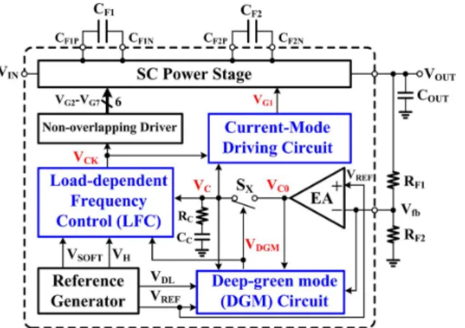
Fig. 4. Proposed SC DC-DC converter with the LFC technique and the DGM circuit.
a result, the performance of both power efficiency and output voltage ripple can be simultaneously guaranteed within a satis-factory range at distinct output load conditions for SoC applica-tions.
The proposed SC DC-DC converter structure is illustrated in Section II. Circuit implementations are described in Section III. Experimental results are shown in Section IV. Finally, a conclu-sion is made in Section V.
II. PROPOSEDSC DC-DC CONVERTERSTRUCTURE AND STABILITYANALYSIS
Fig. 4 shows the proposed SC DC-DC converter structure with two small off-chip flying capacitors, and , to de-liver the energy from the input to the output . To reg-ulate the and to ensure supplying quality for the other cir-cuits in SoC, the voltage divider, composed of and , is used to feedback the output information. Feedback signal compares with the reference voltage by the error amplifier (EA) to generate the pre-error signal . Through the closed-loop operation in normal operation, the error signal con-necting to with the switch can decide the charging time of the flying capacitor and the level of the analog signal to define the driving capability of SC power stage. Therefore, loading current dependent energy control scheme in SC power stage can be realized [20]. The closed-loop control simply uses the proportional-integral (PI) compensation composed of and to generate a low-frequency pole-zero pair to increase system stability.
Due to the loading information contained by the in normal operation, the proposed LFC technique can monitor the trend of loading current during load transient response. Besides, the slope of represents the trend of load condition and is used to generate the system clock for controlling the switching frequency , which represents the switching frequency. The system performance is improved by a trade-off between switching power loss and output voltage ripple.
In other words, the proposed pseudo-clock controlled LFC technique dynamically adjusts the switching frequency ac-cording to the trend of different load condition. When the loading current increases toward heavy condition, the LFC technique gradually increases the to provide high current driving capability and to ensure regulation performance. More-over, the output ripple can be reduced by meanings of increasing . On the other hand, when the loading current suddenly decreases, the LFC technique will accordingly decrease the
Fig. 5. Implementation of SC power stage.
for high efficiency because of reduced switching power loss. Besides, the switching frequency changing between the four operating frequencies (0.5, 1, 2, and 4 MHz) can instantly provide driving current to the output for good load transient performance. It also brings the advantage of reduced EMI to meet the requirement of the SoC. Moreover, the LFC technique uses the reference voltage and the , derived from the reference generator, to calibrate the switching frequency in normal operation and to provide soft-start operation for high reliability in startup period.
On the other hand, the DGM operation is activated at ultra-light loads to effectively enhance power conversion energy if the is smaller than the signal reference voltage . In the meanwhile, the DGM circuit triggers the signal , which masks the switching clock until the output demands for energy replenishment. The also turns off the and clamps the to prevent the cross interference between the normal operation and the DGM operation. In other words, the controller works as a ripple-based control by monitoring output voltage. Furthermore, power conversion efficiency is also guaranteed by the non-overlapping driver, which generates the six-bit signals - to have enough current driving capability and to avoid the shoot through current.
A. SC Power Stage
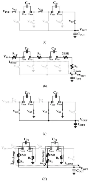
Fig. 5 illustrates the SC power stage, which contains seven power switches to realize 1/3x conversion ratio. The transistor is used as a current source to control the charging current to the flying capacitors while the other transistors work as the power switched. Here, the duty of switching period is fixed as 50%. Basically, the ideal power conversion efficiency is shown as (1).
(1) Due to the step-down operation in the proposed SC converter, the power conversion efficiency is mainly decided by the rela-tionship between the input voltage , the output voltage and the conversion ratio , which is 1/3 in this work.
The simplified dc model of SC converter with the cur-rent-mode driving control is depicted in Fig. 6. Corresponding to the 1/3x SC power stage, it includes the dependent voltage source , the adjusting equivalent resistance , the
output loading , and output capacitor . The
equivalent function contributed by the transistors -is modeled as an equivalent voltage source with a conversion ration . The transistor in SC power stage can work as an adjustable because can control the charging energy by adjusting the gate voltage , which is derived from the current-mode driving circuit. This simplified dc model doesn’t contain the conduction loss, switching loss and the quiescent
Fig. 6. Simplified dc model of the SC power stage with the current-mode driving control.
current loss. Thus, the output voltage can be regulated as a predefined voltage by adjusting the as expressed in (2). If the is far away from the value of due to the increasing loading current , the efficiency will become lower than (1) because large power loss occurs in the voltage drop across the adjustable .
(2) The energy charging and discharging schemes of the SC power stage are illustrated in Figs. 7(a) and (c), respectively. During energy charging phase, the charging current directly flows from the to the through two flying capacitors and . According to different load current, the charging current is controlled by the gate control signal . The re-maining power switches are operated with the driving signals - from the non-overlapping driver to provide correct energy discharging phase. During the energy discharging phase, both the flying capacitors are in parallel connected to the output capacitor for providing enough driving current.
To derive the power loss of the SC converter, Fig. 7(b) and (d) depict the model, which includes the on-resistance of power switch and the ESR of the flying capacitors, in charging phase and discharging phase, respectively. The period of the charging or discharging phase is half of the switching cycle be-cause the duty cycle is fixed at 50%. In Fig. 7(b) and (d), the is equal to the in the charging phase while the is equal to twice the in the discharging phase. Total power loss as shown in (3) includes conduction power
loss , switching power loss , and extra
power loss dissipated by the control circuit. The in (4) is resulted by the power transistors and the ESR. The is caused by charging and discharging the parasitic capacitance parallel to each flying capacitor as expressed in (5).
(3) (4) (5) where is the parallel parasitic capacitance of the -th flying capacitor and is the voltage difference within half of one switching period.
When the system operates at light loads, the total power loss is mainly dominated by the . That is to say, the
can be further reduced if the switching frequency is prop-erly adjusted by the proposed LFC technique. As a result, the efficiency can be effectively improved especially at light and medium loads. Furthermore, small flying capacitor can be used
Fig. 7. (a) Operation in the charging phase. (b) Modeling including conduction loss and ESR resistors in the charging phase. (c) Operation in the discharging phase. (d) Modeling including conduction loss and ESR resistors in the dis-charging phase.
because the can be changed according to the loading cur-rent. Consequently, the caused by the ESR can also be reduced since small flying capacitor accompanies a small ESR. In conclusion, the LFC technique changes the switching frequency according to the loading current can enhance the ef-ficiency.
B. Pseudo-Clock Controlled LFC Operation
The main purpose of LFC technique is to immediately adjust the switching frequency for achieving adequate energy driving capability, high efficiency, and fast transient response for dif-ferent loading current. The output voltage information is delivered to the EA from the voltage divider, and as shown in Fig. 4. Thus, the output of the EA, , reflects the loading current information. In the normal operation, shorts to by turning . Considering the stability, PI compen-sator, composed of compensation resistor and capacitor , is adopted to extend the bandwidth and low-frequency gain for regulation performance. In steady state, the is regulated at one certain voltage level. In case of loading current transient, the driving current capability of power stage will be changed
Fig. 8. The pseudo-clock under different trend of the in LFC tech-nique.
TABLE I
THEILLUSTRATION OFRELATIONSHIPBETWEEN AND
by the variation of . Interestingly, the trend of the varia-tion can be used to indicate the proper trend in the variavaria-tion of switching frequency.
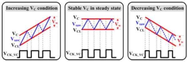
As depicted in Fig. 8, the signal is defined as a pseudo-clock, which is generated by a saw-tooth signal ramping up/down within a pre-defined fixed hysteresis window
. is the upper bound of the hysteresis window. Besides, in steady state, the duty cycle of is 50%. With a fixed hysteresis window, , the trend of the variation can vary the duty of . In case of light-to-heavy load change, the increasing forces the duty of to be larger than 50% since the on-time increases and the off-time decreases. On the other hand, the heavy-to-light loads change forces the duty of smaller than 50%. Consequently, according to the trend of the variation, the difference of is listed in Table I. In other words, wider range of load transient which makes larger voltage variation at the output results in larger duty variation of the .
To obtain adequate energy driving capability by adjusting the switching frequency, the should compare with one pre-defined reference-clock to decide the increase or decrease in the switching frequency as illustrated in Fig. 9. Sim-ilarly, the duty of is fixed at 0.5. Thus, the
synchronizes with the in steady state. One threshold period is utilized to avoid oscillation between two dif-ferent switching frequencies in the LFC technique. In case of light-to-heavy loads change, the duty of is larger than 0.5. If the variation of duty is larger than the value of , the switching frequency will be increased. As depicted in Fig. 9(a), the is increased to a higher value. In other words, the light-to-heavy loads change causes the increase of and thus
makes the lags the with the amount of
lag-ging period since the current switching frequency can’t have the ability to deliver enough energy to the output. After the increase of switching frequency by the LFC technique, the SC converter can provide adequate energy to the output.
Mean-while, the will synchronize with the again
after the output voltage is regulated.
On the other hand, if the loads change from heavy to light, the phase of leads that of . As shown in Fig. 9(b), when the leading time is larger than the , the switching frequency should be decreased to avoid excess energy
Fig. 9. Comparison of and in LFC technique for (a) in-creasing and (b) dein-creasing in switching frequency.
Fig. 10. Small signal model of the proposed SC converter.
delivering to the output. After the adjustment in the switching frequency by the LFC technique, the output voltage will be well-regulated and the will synchronize with the . In conclusion, the proposed pseudo-clock controlled technique reflects the load conditions and the LFC technique features the fast transient response owing to the adjustable switching
fre-quency according to different duty of and .
Furthermore, the SC converter operates with a proper switching frequency for adequate energy driving capability in steady state.
C. System Stability Analysis
The small signal model of the SC converter with the PI com-pensation, which is composed of the resistor and the ca-pacitor , is illustrated in Fig. 10. K is defined as the gain of current-mode driving circuit. G is defined as the gain of power stage of SC converter. The ideal value of G is equal to 1/3 ac-cording to the structure of the switches and flying capacitors. Two poles as expressed in (6) and (7) locate at the output of EA and the output , respectively.
(6) (7) is the equivalent output resistance of the EA and
is the equivalent loading resistance. Besides, one compensated zero contributed by the PI compensation is shown in (8).
(8) The current-mode driving control circuit converts the to the to control the charging current for charging the flying capacitors. Thus, it’s modeled as the combination of the V-I con-verter and the current buffer , which has an equiva-lent output resistance . Therefore, the transfer function of SC converter can be expressed in (9).
Fig. 11. Frequency response of the proposed SC converter.
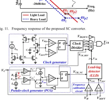
Fig. 12. Schematic of the proposed of LFC circuit.
The frequency response of proposed SC converter is shown in Fig. 11. Because the output pole depends on the load condition, the compensated zero in (8) cancels the lower-frequency output pole at light loads to ensure a sufficiency phase margin (PM). Thus, the pole at the output of EA becomes the dominant pole of the SC converter. Before the unit-gain frequency (UGF), the system simply contains one pole to ensure the stability in the proposed SC converter.
III. CIRCUITIMPLEMENTATION
A. Load-Dependent Frequency Control (LFC) Circuit
Fig. 12 shows the implementation of LFC circuit. To achieve adequate energy driving capability for different output load, the switching frequency in the proposed SC converter can be varied, so as to ensure regulation performance and conversion efficiency. The LFC circuit contains the clock generator, the pseudo-clock generator (PCG), the lead-lag detector (LLD), and the frequency calibration circuit.
The clock generator defines the basic clock and the clock divider produces several clock signals with same duty ratio as 50% but with different frequencies. The lowest frequency of these signals, , is used as a reference-clock. The system-clock is adjustable which is controlled by the LLD circuit to increase or decrease the switching frequency when the loading current increases or decreases, respectively. Further-more, the can be further modulated by the signal for drastically decreasing switching power loss at ultra-light loads.
The is connected to the PCG in order to generate the pseudo-clock with the variable duty cycle corre-sponding to the trend of . In the PCG circuit, the hysteresis window, , is generated by a fixed DC offset formed by the flowing through the resistor . The upper and the lower bounds are and , respectively. Two operational amplifiers, and , are used as the buffer to filter out high frequency noise and to get clean control signals and
. Here, the determination of the on-time of is to compare the saw-tooth , which is generated by charging the capacitor with a constant current , with the upper bound, . On the other hand, the duration of the off-time is decided by the positive edge of the and follows (the buffered output of ). Thus, the LLD circuit can decide the lead or lag condition in Fig. 9 to decrease or in-crease the switching frequency, respectively, by comparing the with the . After the increment or decrement of the switching frequency, the can synchronize the
at the steady state.
The frequency calibration circuit is composed of two com-parators, and , which are used to compare the with the reference voltage and , respectively. If the approaches the in case of increasing loading cur-rent, the gain of the EA is deteriorated because the transistors at the output stage of the EA are in the triode region. Thus, a signal triggered by frequency calibration circuit to the LLD circuit can avoid the failure of the EA by the increase of switching frequency. That is to say, higher switching frequency ensures higher driving capability and has the ability to pull low the level of the until it’s within the range of and . Similarly, if approaches the voltage level of in case of decreasing loads, the frequency calibration circuit triggers the to the LLD circuit to decrease the switching fre-quency. Here, with a lower voltage level works as the function soft-start to prevent the output from being overcharged by much energy injection, which results in drastic variation at the if the output voltage is much lower than its nominal value during start-up period. Namely, the comparison between the with the can decide the signal of to inhibit the switching frequency increasing.
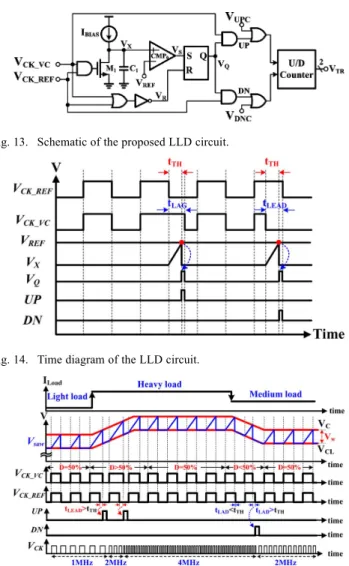
The LLD circuit implementation is depicted in Fig. 13. To avoid abnormal oscillation between two switching frequencies, the threshold period is designed in the LLD circuit. The is determined by the biasing current , the capacitor , and the . When the leading or lagging time of
is greater than the compared to the , the signal of
DN or the UP will be triggered by the logic circuit to activate the
up/down(U/D) counter. Furthermore, when the error signal is failed to generate the slope because its level is near the power supply or ground, the frequency calibration signals and from the frequency calibration circuit can also trigger the U/D counter. Finally, the voltage will be an adequate value in steady state to control the multiplexer which determines the switching frequency of . The time diagram of the LLD cir-cuit is shown in Fig. 14. When the lags the , the signal ramps up by a constant current and compares with the reference voltage , which determines the . Once the lagging time is larger than the , the signal UP is sent to increase the switching frequency. Similarly, the switching fre-quency can be decreased by the signal DN if the leading time is larger than the .
Fig. 15 illustrates the detail time diagram in the pseudo-clock controlled LFC technique by the LLD circuit. When the loading current changes, the error signal will be varied to response to it by the negative feedback control. Different load steps result in different variations and the changes in the duty of
which is realized by the PCG. It’s indicated as mentioned in Table I. Then, the comparison of the and the
is implemented in the LLD circuit to determine the adequate frequency by controlling . When the loads changes from light to heavy, the duty of is larger than the duty of
Fig. 13. Schematic of the proposed LLD circuit.
Fig. 14. Time diagram of the LLD circuit.
Fig. 15. Time diagram in the pseudo-clock controlled LFC technique by the LLD circuit.
by the extra period . When the is longer than the , insufficient energy supply derived at the output will result in the increment of switching frequency to guarantee a well-regulated output voltage. That is, the signal UP will be set as logic high to activate the U/D counter. Therefore, the will be increased to select the higher switching frequencies as
until enough energy can be transferred to the output. On the other hand, the decreasing switching frequency will happen
when the phase of leads that of higher than
the value of in case of heavy-to-light loads.
B. Current-Mode Driving Circuit
Fig. 16 shows the current-mode driving circuit to drive the power switch for controlling the energy driving scheme of the proposed SC converter. The error signal can be utilized to determine how large the driving current can be sourced from the since the derived from the output of EA contains the load information. The transferred from through V-I conversion will be magnified through the three-stage cascaded current mirrors to guarantee the demanded current driving ca-pability. The advantage is the can be regarded as the cur-rent source with small voltage headroom requirement at the en-ergy charging phase. On the other hand, the signal gener-ated by the LFC circuit will turn off the to stop the energy charging for the flying capacitor when the SC converter operates at the discharging phase. Moreover, another advantage is that
Fig. 16. Schematic of the proposed current-mode driving circuit.
Fig. 17. Schematic of the proposed DGM circuit for ultra-light load condition. the turning-off operation of the does not need a large size of to disable the power switch due to the three-stage cascaded current mirrors. Besides, the value of and K is design as 10, 10, and 400, respectively for reasonable consider-ation of acceptable power loss and frequency response. That is, the power loss consumed by the current-mode driving circuit is only about 0.2775% of total power and it brings less deteriora-tion of total power efficiency.
C. Deep-Green Mode (DGM) Operation
To maintain high power conversion efficiency at ultra-light loads, the DGM circuit as depicted in Fig. 17 can be utilized to mask the switching clocks to reduce switching power loss. When the pre-error signal is lower than a threshold voltage level , the DGM operation will be activated by triggering the signal . Thus, the system is operating by ripple-based control and the output voltage is monitored by the hysteresis comparator to guarantee the output voltage regulation. More-over, the signal is disconnected to EA and clamped at voltage by the error-clamping circuit (ECC) which is used to structure a feedback loop. The and the can be used to increase the circuit stability. The clamped voltage
is defined by the through the source follower . The gate-source voltage of works as the hysteresis voltage to avoid incorrect toggle between the DGM and the normal op-eration. Clamping function aims to prevent the cross interfer-ence between the linear loop of current driving capability in the normal operation and the ripple-based control in the DGM op-eration.
IV. EXPRIMENTALRESULTS
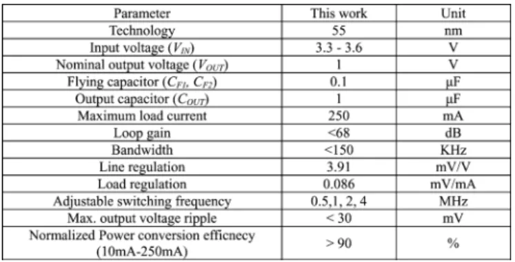
The proposed SC DC-DC converter with the LFC and DGM techniques was fabricated in 55 nm CMOS process for SoC integration. The input voltage ranges from 3.3 V to 3.6 V. The nominal output voltage is 1 V to supply the core de-vices in 55nm technology. More importantly, the flying capac-itors and the output capacitor can be used as small as 0.1 F and 1 F, respectively. The maximum loading current is 250 mA. The design specifications of proposed SC converter are listed in Table II. The chip micrograph with active area of 1100
Fig. 18. Chip micrograph of the proposed SC converter.
Fig. 19. Prototype of the proposed SC converter. TABLE II DESIGNSPECIFICATIONS
m 1200 m is shown in Fig. 18. The prototype of the pro-posed SC converter is shown in Fig. 19. Obviously, with in-ductor-less architecture of the proposed SC converter, the PCB cost is as less as possible with regardless of the other testing components.
Fig. 20 demonstrates the measured steady-state operation with different switching frequencies under different load con-ditions when the input and regulated output voltage are 3.3 V and 1 V, respectively. The , which is the positive terminal of the flying capacitor in Fig. 4, shows the switching frequency is 500 kHz in Fig. 20(a). Due to light load condition, the switching frequency is actually reduced to a smallest value for power saving. The power conversion efficiency is kept higher than 84%. Simultaneously, the output ripple can be
Fig. 20. Measured steady-state operation with different switching frequencies under different load conditions. (a) mA. (b) mA.
(c) mA.(d) mA.
effectively controlled within 30 mV. Similarly, Figs. 20(b)-(d) show increasing switching frequency from 1 M to 4 M owing to the increase at loading current from 35 mA to 224 mA. Furthermore, the output voltage ripple can be kept smaller than 25 mV because the output voltage ripple can be reduced by increasing the switching frequency.
Fig. 21 shows the completely measured load transient re-sponse between medium and light loads with distinct switching frequencies. The is the signal of the negative terminal of the flying capacitor in Fig. 4. When the changes from 70 mA to 25 mA, the switching frequency is adjusted from 1 MHz to 500 kHz with the output voltage ripples, 25 mV and 30 mV, respectively. The performance can also be maintained when the changes from 25 mA back to 70 mA. The recovery times of overshoot and undershoot are 5 s and 20 s, respec-tively. Good voltage regulation and fast transient response are achieved because of high loop gain and bandwidth. Fig. 22(a) can demonstrate the details of the LFC technique mechanism. The LFC contains the comparative operation of two clocks, and to determine the frequency. Fig. 22(b) shows the duty of is smaller than that of the
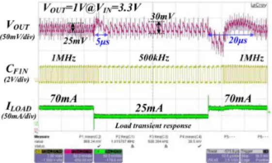
Fig. 21. Measured load transient response between 70 mA and 25 mA with adjusted switching frequencies.
Fig. 22. Measured load transient response with the LFC techinque. (a) Load transient response from 70 mA to 25 mA. (b) Load transient response from 70 mA to 25 mA. (c) Load transient response from 25 mA to 70 mA.
Fig. 22(c). As expected, the switching frequency changes if the or the is greater than the .
The load transient response with both step-up and step-down between middle and heavy loads is depicted in Fig. 23(a). As shown in Figs. 23(b) and (c), the switching frequency will in-crease or dein-crease by the LFC technique as 1 MHz and 2 MHz with the loading current of 70 mA and 130 mA, respectively. The output ripple can be decreased when the switching fre-quency increases. The recovery time is about 7 s for under-shoot and about 12 s for overunder-shoot. Fig. 24 shows the DGM operation for enhancing the ultra-light load efficiency if load current is 10 mA. Meanwhile, the output voltage ripple can be kept within 30 mV.
The measured normalized power conversion efficiency and the output ripple with or without the proposed LFC and DGM
Fig. 23. Measured load transient response with LFC techinque (a) load tran-sient between 70 mA to 130 mA (b) load trantran-sient from 70 mA to 130 mA (c) load transient from 130 mA to 70 mA.
Fig. 24. Measured load transient response from 50 mA to 10 mA with the DGM control.
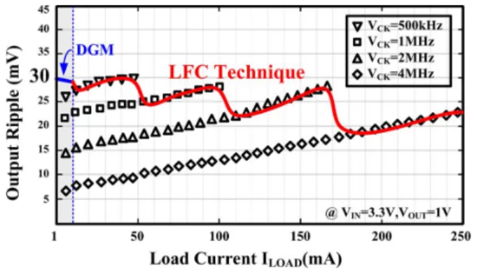
controls are shown in Figs. 25 and 26, respectively. According to (1) with the designed and , the ideal efficiency is 91%. The switching loss can be greatly reduced owing to the proposed LFC and DGM controls. The measured peak ef-ficiency increases to 89%, which is equal to 98% normalized efficiency, when the is 100 mA and the overall normal-ized efficiency is maintained higher than 90% from 10 mA to 250 mA. The output voltage ripple becomes larger during the light-to-heavy loads change under the operation with a constant switching frequency. That is, the ripple can also be minimized by increasing the switching frequency and guaranteed smaller than 30 mV with smaller flying capacitors and output capacitor compared to the commercial products. Finally, the comparisons of the prior SC methodologies are shown in Table III.
V. CONCLUSION
The pseudo-clock controlled LFC SC DC-DC converter with the DGM operation is proposed to achieve high efficiency over a wide load range for power management in SoC applications.
TABLE III
COMPARISONTABLEWITH THEPRIORARTS
Fig. 25. Measured normalized power conversion efficiency w/i and w/o the proposed LFC and DGM techniques.
Fig. 26. Measured output voltage ripple w/i and w/o the proposed LFC and DGM techniques.
Besides, small flying capacitors with smaller ESR can be uti-lized to reduce the switching power loss because the switching frequency can be adjusted according to the load condition. Furthermore, without using the inductor-based power manage-ment solution, minimization in PCB area and cost reduction can be achieved. The 1/3X step-down SC operation with the current-mode driving control forms a closed-loop function for modulating the output voltage. In addition, the LFC adjusts the
switching frequency according to the distinct load condition which is reflected by PCG to ensure high efficiency and good voltage regulation over a wide load range. The load-depen-dent frequency can also improve the transient response and is demonstrated in measurement results. Furthermore, the DGM operation further helps enhance the power conversion efficiency at ultra-light loads. Measurement results show the normalized efficiency can be maintained over 90% and the output voltage ripple can be guaranteed smaller than 30 mV.
REFERENCES
[1] Y.-H. Lee, Y.-Y. Yang, K.-H. Chen, Y.-H. Lin, S.-J. Wang, K.-L. Zheng, P.-F. Chen, C.-Y. Hsieh, Y.-Z. Ke, Y.-K. Chen, and C.-C. Huang, “A DVS embedded power management for high efficiency integrated SoC in UWB system,” IEEE J. Solid-State Circuits, vol. 45, no. 11, pp. 2227–2238, Nov. 2010.
[2] C.-C. Wang and J.-C. Wu, “Efficiency improvement in charge pump circuits,” IEEE J. Solid-State Circuits, vol. 32, no. 6, pp. 852–860, Jun. 1997.
[3] T. Ying, W.-H. Ki, and M. Chan, “Area-efficient CMOS charge pumps for LCD drivers,” IEEE J. Solid-State Circuits, vol. 38, no. 10, pp. 1721–1725, Oct. 2003.
[4] R. Pelliconi, D. Iezzi, A. Baroni, M. Pasotti, and P. L. Rolandi, “Power efficient charge pump in deep submicron standard CMOS technology,”
IEEE J. Solid-State Circuits, vol. 38, no. 6, pp. 1068–1071, Jun. 2003.
[5] P. Favrat, P. Deval, and M. J. Declercq, “A high-efficiency CMOS voltage doubler,” IEEE J. Solid-State Circuits, vol. 33, no. 3, pp. 410–416, Mar. 1998.
[6] H. Lee and P. K. T. Mok, “Switching noise and shoot-through current reduction techniques for switched-capacitor voltage doubler,” IEEE J.
Solid-State Circuits, vol. 40, no. 5, pp. 1136–1146, May 2005.
[7] M.-D. Ker, S.-L. Chen, and C.-S. Tsai, “Design of charge pump cir-cuit with consideration of gate-oxide reliability in low-voltage CMOS processes,” IEEE J. Solid-State Circuits, vol. 41, no. 5, pp. 1100–1107, May 2006.
[8] H. Lee and P. K. T. Mok, “An SC voltage doubler with pseudo-contin-uous output regulation using a three-stage switchable opamp,” IEEE J.
Solid-State Circuits, vol. 42, no. 6, pp. 1216–1229, Jun. 2007.
[9] B. R. Gregoire, “A compact switched-capacitor regulated charge pump power supply,” IEEE J. Solid-State Circuits, vol. 41, no. 8, pp. 1944–1953, Aug. 2006.
[10] J.-Y. Lee, S.-E. Kim, S.-J. Song, J.-K. Kim, S. Kim, and H.-J. Yoo, “A regulated charge pump with small ripple voltage and fast start-up,”
switching power supply with adaptive on-time pulse-frequency modu-lation (PFM) control,” IEEE Trans. Circuits Syst. I, Reg. Papers, vol. 54, no. 2, pp. 312–321, Feb. 2007.
[14] H.-W. Huang, C.-C. Chien, K.-H. Chen, and S.-Y. Kuo, “Highly effi-cient tri-mode control of buck converters with load sensing technique,” in Proc. IEEE Power Electron. Specialists Conf., Jun. 2006, pp. 1–4. [15] L.-K. Chang and C.-H. Hu, “High efficiency MOS charge pumps based
on exponential-gain structure with pumping gain increase circuits,”
IEEE Trans. Power Electron., vol. 21, no. 3, pp. 826–831, May 2006.
[16] Y.-P. Su, Y.-C. Chen, H.-H. Huang, Y.-H. Lee, Y.-Y. Yang, K.-H. Chen, M.-J. Du, and S.-H. Cheng, “Current-mode synthetic control (CSC) technique for high efficiency DC-DC boost converters over a wide load range,” in Proc. IEEE Int. Symp. Circuits Syst. (ISCAS), May 2011, pp. 933–936.
[17] Y. K. Ramadass, A. A. Fayed, and A. P. Chandrakasan, “A fully-In-tegrated switched-capacitor step-down DC-DC converter with digital capacitance modulation in 45 nm CMOS,” IEEE J. Solid-State
Cir-cuits, vol. 45, no. 12, pp. 2557–2565, Dec. 2010.
[18] H.-P. Le et al., “A 32 nm fully integrated reconfigurable switched-ca-pacitor DC-DC converter delivering 0.55 W/mm at 81% efficiency,” in IEEE ISSCC Dig. Tech. Papers, Feb. 2010, pp. 210–211. [19] X. Zhang and H. Lee, “An efficiency-enhanced auto-reconfigurable
2X/3X SC charge pump for transcutaneous power transmission,” IEEE
J. Solid-State Circuits, vol. 45, no. 9, pp. 1906–1922, Sep. 2010.
[20] M.-H. Huang, P.-C. Fan, and K.-H. Chen, “Low-ripple and dual-phase charge pump circuit regulated by switched-capacitor-based bandgap refence,” IEEE Trans. Power Electron., vol. 24, no. 5, pp. 1161–1172, May 2009.
[21] V. Ng and S. Sanders, “A 92%-efficiency wide-input-voltage-range switched-capacitor DC-DC converter,” in IEEE ISSCC Dig. Tech.
Pa-pers, Feb. 2012, pp. 528–620.
[22] S.-C. Tan et al., “Adaptive mixed on-time and switching frequency control of a system of interleaved switched-capacitor converters,”
IEEE Trans, Power Electron., vol. 26, no. 2, pp. 364–380, Feb. 2011.
[23] H.-K. Kwan, D. C. W. Ng, and V. W. K. So, “Design and analysis of dual-mode digital-control step-up switched-capacitor power con-verter with pulse-skipping and numerically controlled oscillator-based frequency modulation,” IEEE Trans. Very Large Scale Integr. (VLSI)
Syst., vol. 21, no. 11, pp. 2132–2140, Nov. 2013.
Wei-Chung Chen (S’12) was born in Yunlin, Taiwan. He received the B.S. degree from the Department of Electrical Engineering, National Sun Yat-sen University in 2010, and M.S. degree from National Chiao Tung University in 2012. He is currently pursuing the Ph.D. degree in the Institute of Electrical and Computer Engineering, National Chiao Tung University, Hsinchu, Taiwan.
He is a member of the Mixed-Signal and Power Management IC Laboratory, Institute of Electrical and Computer Engineering, National Chiao Tung University, Hsinchu, Taiwan. His research interests include the power manage-ment IC design, analog integrated circuits, and mixed signal IC design.
Da-Long Ming was born in Namhsan, Myanmar. He received the B.S. degree from the Department of Electrical Engineering, National Cheng Kung University, Tainan, Taiwan, in 2010, and the M.S. degree from the Department of Electrical Engi-neering, National Chiao Tung University, Hsinchu, Taiwan, in 2012.
He is a member of the Mixed Signal and Power Management IC Laboratory at National Chiao Tung University. His research interests include the power management IC design, the LED driver IC design and
siung, Taiwan, in 2009. She is currently working to-ward the Ph.D. degree at the Institute of Electrical En-gineering, National Chiao Tung University, Hsinchu, Taiwan.
She is a Member in the Mixed Signal and Power Management IC Laboratory, Institute of Electrical Engineering, National Chiao Tung University. Her current research interests include the power management and analog integrated circuits design.
Yu-Huei Lee (S’09) was born in Taipei, Taiwan. He received the B.S. and M.S. degrees from the Department of Electrical and Control Engineering, National Chiao Tung University, Hsinchu, Taiwan, in 2007 and 2009, respectively, and the Ph.D. degree from the Institute of Electrical Control Engineering, National Chiao Tung University, Hsinchu, Taiwan, in 2012.
He is a member at the Mixed Signal and Power IC Laboratory, Institute of Electrical Control Engi-neering, National Chiao Tung University, Hsinchu, Taiwan. His current research interests include the power management integrated circuit design, light-emitting diode driver IC design, and analog integrated cir-cuits.
Ke-Horng Chen (M’04–SM’09) received the B.S., M.S., and Ph.D. degrees in electrical engineering from National Taiwan University, Taipei, in 1994, 1996, and 2003, respectively.
From 1996 to 1998, he was a part-time IC Designer at Philips, Taipei, Taiwan. From 1998 to 2000, he was an Application Engineer at Avanti, Ltd., Taiwan. From 2000 to 2003, he was a Project Manager at ACARD, Ltd., where he was engaged in designing power management ICs. He is currently a Director of the Institute of Electrical Control Engineering and a Professor of the Department of Electrical Engineering, National Chiao Tung University, Hsinchu, Taiwan, where he organized a Mixed-Signal and Power Management IC Laboratory. He is the author or coauthor of more than 100 papers published in journals and conferences, and also holds several patents. His current research interests include power management ICs, mixed-signal circuit designs, display algorithm and driver designs of liquid crystal display (LCD) TV, red, green, and blue (RGB) color sequential backlight designs.
Dr. Chen has served as an Associate Editor of the IEEE TRANSACTIONS ON POWER ELECTRONICS and IEEE TRANSACTIONS ON CIRCUITS AND
SYSTEMS—PARTII: EXPRESSBRIEFS. He also joined Editorial Board of Analog Integrated Circuits and Signal Processing in 2013. He is on the IEEE Circuits and Systems (CAS) VLSI Systems and Applications Technical Committee, and the IEEE CAS Power and Energy Circuits and Systems Technical Committee. He is on the Society for Information Display (SID) and International Display Manufacturing Conference (IDMC) Technical Program Sub-committees. He is the Tutorial Co-Chair of IEEE Asia Pacific Conference on Circuits and Systems (2012 APCCAS). He is the Task Chair of Integrated Power Electronics of IEEE International Conference on Power Electronics and Drive Systems (PEDS) 2013. He is a Technical Program Co-Chair of IEEE International Future Energy Electronics Conference (IFEEC) 2013.