國 立 交 通 大 學
電信工程研究所
碩 士 論 文
設計低相位雜訊四相位震盪器與高增益降頻混頻器
Design of Low Phase Noise Quadrature VCO and High Gain
Down Conversion Mixer
研究生:賴星翰
指導教授:周復芳 博士
設計低相位雜訊四相位震盪器與高增益降頻混頻器
Design of Low Phase Noise Quadrature VCO and High Gain Down
Conversion Mixer
研究生:賴星翰 Student:Hsing-Han Lai
指導教授:周復芳 博士 Advisor:Dr. Christina F. Jou
國 立 交 通 大 學
電 信 工 程 研 究 所
碩 士 論 文
A Thesis
Submitted to Institute of Communication Engineering
College of Electrical and Computer Engineering
National Chiao Tung University
in Partial Fulfillment of the Requirements
for the Degree of Master
in
Communication Engineering
July 2012
Hsinchu, Taiwan, Republic of China
設計低相位雜訊四相位震盪器與高增益降頻混頻器
研究生:賴星翰 指導教授:周復芳 博士 國立交通大學電信工程研究所碩士班 中 文 摘 要 本 論 文 討 論 分 為 兩 部 分 , 其 中 所 提 出 電 路 之 晶 片 製 作 皆 由 TSMC 0.18 μm mixed-signal/RF CMOS 1P6M 製程來實現。 第一部分為結合電流再利用電路並利用考畢茲電容耦合產生四相位之震盪器。此四 相位震盪器存有這兩種電路的優點,且從模擬中可得到利用電容耦合產生四相位並不會 產生額外的相位雜訊之結論。根據量測結果顯示:本 QVCO 震盪頻率為 4.57~5.02 GHz, 在供應電壓為 1.8 V 之條件下,功率損耗約為 8.46 mW,相位雜訊為-119 dBc/Hz @1 MHz, 而 figure-of-merit (FOM)則為-183.7 dBc/Hz。 第二部分則提出低雜訊放大器運用在混頻器的射頻轉導級的高增益混頻器,這種整 合型態的混頻器,利用低雜訊放大器的功能,可以同時在一個混頻器中達成高增益與低 功率損耗的優點,並且減少面積使用以及避免多個電路整合到單一晶片時所遇到的匹配 問題。第三章電路從分析混頻器各個區塊以達到高增益以及低雜訊,量測時,匹配的 S 參數 14~20 GHz 皆在 -10 dB 以下,12~16 GHz增益頻段中有 18.327 dB的最高轉換增益, 而雜訊指數最小值 13.2 dB,三階截斷點為 - 7.5 dB,而功率損耗為 7.56 mW,FOM 為 191.42;第四章中除了包含第三章設計方法外,在射頻轉導級並接兩個 CCC CG-LNA 和 CS-LNA 以達到寬頻中也具有高增益與低雜訊,量測的 S 參數從 4 GHz 到 20 GHz 皆在 -8 dB 之下。在 2.7~17.8 GHz 增益頻段中只有 22.7 dB 的最高轉換增益,而雜訊指數最小值 10.45 dB,三階截斷點為 -10 dB,而功率損耗為 12.058 mW,FOM 為 192.04。Design of Low Phase Noise Quadrature VCO and High Gain Down
Conversion Mixer
Student:Hsing-Han Lai Advisor:Dr. Christina F. Jou
Department of Communication Engineering National Chiao Tung University
Abstract
This paper consists of two parts. All the proposed circuits were implemented in TSMC 0.18μm mixed-signal/RF CMOS 1P6M technology.
Part I presents a Colpitts current-reused QVCO based on capacitor coupling. The proposed QVCO exists the advantages of Coltpitts and current-reused circuit. Furthermore, using capacitor coupling to generate quadrature signals doesn't make extra phase noise. According to the measured results, the oscillation frequency is 4.57~5.02 GHz, and the power consumption is about 8.46 mW at the supply voltage of 1.8 V. The phase noise at 1 MHz offset is -119 dBc/Hz and the figure-of-merit (FOM) of the proposed QVCO is about -183.7 dBc/Hz.
Part II proposes a high gain mixer with low noise amplifier (LNA) in the RF trans-conductance stage of mixer. Using the ability of LNA, this integrated mixer can achieve high conversion gain and low power consumption in one circuit. Furthermore, it reduces the area and avoids the problem of matching that many components integrate in SOC. In chapter 3, analyzing each block of mixer achieve high conversion gain and low noise figure. During measurement, the matching s-parameter is below -10 dB in 14~20 GHz. The measured bandwidth of conversion gain ranges from 12 to 16 GHz and the maximum gain is 18.3 dB at
14 GHz. The minimum noise figure is 13.2 dB. The measured linearity shows that IIP3 is -7.5 dB. The power consumption is 7.56 mW and the FOM is 191.42;In chapter 4, including the analytic method of chapter 3, constructing cascade construction by CCC CG-LNA and CS-LNA at the RF trans-conductance stage achieves high conversion gain and low noise figure in wide band. The measured s-parameter is below -8 dB in 4~20 GHz. The measured bandwidth of conversion gain covers from 2.7 to 17.8 GHz and the maximum gain is 22.7 dB at 4 GHz and 16 GHz. The minimum noise figure is 10.45 dB. The measured linearity shows that IIP3 is -10 dB. The power consumption is 12.058 mW and the FOM is 192.04。
Acknowledgement
學生碩士班論文能夠順利在兩年完成,首先絕對地要感謝周復芳教授,在交大的求 學生涯中,教授除了傳授我該如何做研究之外,更提供了一個良好的實驗室環境讓我可 以在此自由的發揮所長,而且初窺長遠性思考以及如何待人接物是我在碩士班生活中另 一個收穫。接著,非常感謝張志揚教授以及吳霖堃教授撥空擔任學生的口試委員,教授 們的寶貴建議,使得此次碩論能更加的完整。 在 919 實驗室的歡樂時光裡,一開始要先感謝沈宜星學長(爽哥),爽哥是帶領我們 IC 組的博班學長,在他帶領之下,我擁有相當的自由能做自己有興趣的電路,並且由於 他的協助,讓我投上人生第一篇的研討會論文;接著,是黃玠瑝學長(Double),雖然他 是帶領天線組的博班學長,但多虧他的引領,我才有幸加入 919 這個大家族與 919 成員 共同奮鬥,說到奮鬥,他總是最晚離開 919,他真得好好顧身體阿;再來,是林智鵬學 長(智鵬)和楊超舜學長(舜哥),可能在研究方面是沒有互相接觸到,但我們卻是一起在 運動場上揮灑、一起聊人生方向的好夥伴。 從博班之後,再來感謝的就是碩班的學長姐、同學以及學弟妹,首先要感謝邱柏儒 學長(九哥)和游豐榮學長(威威),九哥教會了我如何模擬射頻電路,威威指導了我關於 RFIC 設計的觀念以及經驗,但最主要的感謝,並不是關於研究的主題,而是人生的主 題,是他們告訴我人生的追求和他們的人生經驗,這些讓我了解到自己該如何去抉擇研 發替代役,更遠地,知道了未來工作的選擇;接著,是曾珮玲(股姐)、林子淵(子淵)、 李政廷(李哥)、呂政浩(卡爺),有股姐在的地方就有歡笑聲,有子淵在的地方就有遊戲 聲,李哥在地方就有瀟灑的風聲,卡爺在的地方就有他真誠的獨特聲,或許不懂的人不 清楚我這段是在說明什麼,但與他們相處過的人,一定可以藉由這些聲音懷念他們在 919 的身影;再來,是牟家宏(阿牟)、林易懋(數理易懋)、黃建榮(建榮),雖然與天線組的易 懋和建榮以及辛苦埋首在 LNA 世界的阿牟在研究上沒有特別的火花,但是在修課以及 919 生活裡增添不少歡樂,尤其感謝易懋,建立了這麼完善的 FTP,讓我們可以在上面取得自己所需的檔案,而看到建榮找到自己人生的心靈寄託也著實替他感到安慰,對於 阿牟我打從心裡面的想封你一個 LNA 神人的稱號;最後,是戴瑜秀(阿秀)、張雨翔(阿 翔)、陳寶國(助教)、朱佑祥(大師)、潘玠倫、馮盛(盛!)、蔡涵婷(八妹),能與你們相處 讓我了解以前當學長們的心態是怎麼一會事,雖然我跟你們相處的時間指導佔居多,聊 天較少,但教學是相長的事情,我也從你們身上學到不少東西,很開心的能認識你們。 除了碩班同學們以外,我也要感謝 CIC 的工作同仁們,劭冠、薪如、恆茹、政宏、 思豪、雅文、烈全、聖文、靖淵、茗航、嘉弘、喬盛...等,因為有了你們的指導與幫忙, 讓我學到更多 RF 相關實際量測的知識與實作,使我在設計時更能注意到更多細節,但 除了學習外,讓我感受最深的是在有你們的環境中,我很快樂並且很享受這份工作,非 常感謝你們。 最後,一定要感謝我的家人以及女朋友,爸爸媽媽以及弟弟是你們建立了這一個溫 暖的家,讓我可以全心投入研究中不被經濟問題所苦,雖然父親常常飛國外出差,但我 知道你的心是想念著家的;以前的我不懂得珍惜母親做的菜,但離開了台北,卻總是在 期待周末回到家能吃到這簡單的家常菜;我感謝我弟弟在我不在家裡時,能一併擔起我 孝順父母的責任,雖然我回到家中也少與你單獨相處,但我相信我們兄弟情誼卻不會因 此淡化掉;孟昀,能夠認識妳是我最大的幸運,也是妳才讓我對生命省思有了改變,雖 然念研究所的時間大部分都是在做研究,不比念大學時能常與妳相聚,但因為有妳在我 身邊,讓我在研究疲乏與困境中有個女孩願意陪伴著我,無法想像妳不在我身邊我是否 還能使我的研究所生涯更加完整。 碩論的篇幅不夠我一一對我生命中其他的朋友致謝,我只能學陳之籓-要感謝的人 太多,那就謝天吧! 賴星翰 於 新竹交通大學 2012 年 夏
Contents
Chinese Abstract ... I Abstract ... II Acknowledgement ... IV Contents ... VI List of Figures ... VIII List of Tables ... X
Chapter 1 ... 1
Introduction ... 1
-1.1 Background and Motivation ... - 1 -
1.2 Phase Noise ... - 4 -
1.3 Thesis Organization... 16
Chapter 2 ... 17
-A Colpitts Current-Reused QVCO Based on Capacitor Coupling...- 17 -
2.1 Introduction ... 17
-2.2 Circuit Design Consideration ... 22
-2.3 Chip Layout and Simulation Results ... 26
-2.4 Measurement Results and Discussion ... 30
Chapter 3 ... 36
A High Gain Down Conversion Mixer in Ku Band ... 36
-3.1 Introduction ... 36
-3.2 Circuit Design Consideration ... 38
-3.3 Simulated and Measured Results ... 41
Chapter 4 ... 49
4 17 GHz Wideband High Gain Down Conversion Mixer with Cascade Structure ... 49
-4.2 Circuit Design Consideration ... 50
-4.3 Simulated and Measured Results ... 54
-Chapter 5 ... - 61 -
Conclusion and Future Work ... 61
-5.1 Conclusion ... 61
-5.2 Future Work ... 62
-List of Figures
Fig. 1 - 1 The diagram of downlink ... - 2 -
Fig. 1 - 2 Block diagram of phase-locked loop ... - 3 -
Fig. 1 - 3 The phase noise per unit bandwidth ... - 4 -
Fig. 1 - 4 A typical phase noise plot for a free running oscillator ... - 5 -
Fig. 1 - 5 Impulse response of an ideal LC oscillator ... - 6 -
Fig. 1 - 6 The equivalent system for ISF decomposition ... - 8 -
Fig. 1 - 7 Conversion of a low frequency sinusoidal current to phase ... - 9 -
Fig. 1 - 8 Conversion of a tone in the vicinity of ωo... - 9 -
Fig. 1 - 9 Conversion of circuit noise to excess phase, and then to phase-noise - 11 - Fig. 1 - 10 S( ) on a log-log axis ... - 13 -
Fig. 2 - 1 Examples of quadrature signal generation methods - quadrature coupling...- 17 -
Fig. 2 - 2 Schematic of the parallel-coupled QVCO (P-QVCO) topology ... - 18 -
Fig. 2 - 3 Schematic of the conventional current-reused topology ... - 19 -
Fig. 2 - 4 Schematic of another conventional current-reused topology ... - 20 -
Fig. 2 - 5 Schematic of Colpitts VCO topology ... - 21 -
Fig. 2 - 6 The equation (2.2) of inductor... - 23 -
Fig. 2 - 7 The inductance and conductance of inductor ... - 23 -
Fig. 2 - 8 Schematic of proposed half circuit ... - 24 -
Fig. 2 - 9 Schematic of a Colpitts current-reused QVCO based on capacitor coupling ... - 25 -
Fig. 2 - 10 Chip layout of the proposed QVCO ... - 26 -
Fig. 2 - 11 The comparison of pre-simulated phase noise at 5GHz ... - 27 -
Fig. 2 - 12 Simulated tuning range of the proposed QVCO...- 28 -
Fig. 2 - 13 Simulated phase noise of the proposed QVCO ... - 29 -
Fig. 2 - 14 Simulated swing of the proposed QVCO ... - 29 -
Fig. 2 - 15 Signal Source Analyzer (Agilent E5052B) ... - 30 -
Fig. 2 - 16 Digital Signal Analyzer (Agilent DSA91204A) ... - 31 -
Fig. 2 - 17 Chip photo of the proposed QVCO ... - 31 -
Fig. 2 - 18 Photograph of the probe station... - 32 -
Fig. 2 - 19 Measured phase noise of the proposed QVCO ... - 33 -
Fig. 2 - 20 Measured output spectrum of the proposed QVCO ... - 33 -
Fig. 2 - 21 Measured voltage swings of the proposed QVCO ... - 33 -
Fig. 3 - 1 Conventional double-balanced mixer...- 36 -
Fig. 3 - 2 Conventional double-balanced mixer with current bleeding ... - 37 -
Fig. 3 - 3 The proposed high gain mixer ... - 38 -
Fig. 3 - 4 The block diagram of conventional mixer ... - 38 -
Fig. 3 - 5 The active load by CMFB circuit ... - 39 -
Fig. 3 - 6 The switch pairs and current bleeding circuit ... - 39 -
Fig. 3 - 7 The LNA trans-conductors for mixer ... - 40 -
Fig. 3 - 8 The chip layout photograph of the proposed high gain mixer...- 41 -
Fig. 3 - 9 The full chip photograph of integrated circuit ... - 42 -
Fig. 3 - 10 The input return loss of the proposed high gain mixer ... - 43 -
Fig. 3 - 11 The conversion gain of the proposed high gain mixer... - 43 -
Fig. 3 - 12 The noise figure of the proposed high gain mixer ... - 44 -
Fig. 3 - 13 The P1dB of the proposed high gain mixer ... - 45 -
Fig. 3 - 14 The IIP3 of the proposed high gain mixer ... - 46 -
Fig. 3 - 15 The isolation of the proposed high gain mixer ... - 46 -
Fig. 4 - 1 The proposed high gain mixer with wideband gamplifier...- 50 -
Fig. 4 - 2 The CS-LNA with series RLC input match network ... - 51 -
Fig. 4 - 3 The structure of common gate amplifier... - 52 -
Fig. 4 - 4 The structure of CCC CG-LNA ... - 53 -
Fig. 4 - 5 The chip layout of the proposed mixer ... - 54 -
Fig. 4 - 6 The chip photograph f the proposed mixer...- 55 -
Fig. 4 - 7 The input return loss of the proposed mixer ... - 56 -
Fig. 4 - 8 The conversion gain of the proposed mixer...- 56 -
Fig. 4 - 9 The noise figure of the proposed mixer ... - 56 -
Fig. 4 - 10 The P1dB of the proposed mixer ... - 57 -
Fig. 4 - 11 The IIP3 of the proposed mixer ... - 58 -
Fig. 4 - 12 The isolation of the proposed mixer ... - 58 -
List of Tables
Table 2 - 1 Simulated results of the proposed QVCO ... - 35 -
Table 2 - 2 Comparison of QVCO performance ... - 35 -
Table 3 - 1 Simulated results of the proposed high gain mixer ... - 47 -
Table 3 - 2 Comparison of mixer performance ... - 48 -
Table 4 - 1 Simulated and measured result of the proposed mixer...- 59 -
Chapter 1
Introduction
1.1
Background and Motivation
As increasing demand for wireless communications system, the requirements of low-cost and low power consumption for wireless system have dramatically increased. Also, it is required to reduce the circuit size and cost. Thus, we need an advanced integration to design Integrated Circuit (IC) in small area. In addition to area and cost, it is very significant to decrease the voltage supply and the power consumption. Wireless systems for many standards, including GSM, Bluetooth, WLAN, and Wireless Personal Area Network (WPAN) require low power consumption design techniques to enhance the battery lifetime and to improve their integration. Moreover, the development of advanced CMOS technology with the short-channel length is achieving higher cut-off frequency. Instead of BJT and GaAs (Gallium Arsenide), CMOS is very attractive for RFIC due to the capability of system-on-chip (SOC) implementation. Furthermore, scaling CMOS technology also satisfies the requirement of low-cost and smaller size.
In one kind of communication systems, downlink is a term in telecommunications that is used to refer to a data transmission in which data flows from an orbital satellite receiver to a ground-based transmitter. When a ground-based transmitter transmits data to a satellite in Earth’s orbit, shown in Fig. 1 -1, the satellite stores the information until it can decide what to do with it. Downlink is usually used in astronomy, radio science, and telecommunications [1].
Downlink transmits to the C Band (3.7~4.2 GHz), the Ku Band (11.7~12.7 GHz ), and the Ka Band between (18.3~20.2 GHz). The downlink applications in C Band radio frequencies are used to transmit data through thick rain clouds and other adverse weather conditions, which can often disrupt data. Ku Band radio frequencies are used to transmit data to small ground-based satellite dishes, such as those found on rooftops, and generally use more energy than C Band frequencies. Likewise, Ka Band radio frequencies are used to transmit data to small satellite dishes, but are specifically used for broadcasting satellite television and Internet [1].
Fig. 1 - 1 The diagram of downlink [1]
The wireless communication standards generally use phase or frequency modulation, which require quadrature local signals mixing to extract the information contained in both sides of the spectra [2]. Phase-locked loop (PLL) is widely utilized to be a source of local oscillation signal, as shown in Fig. 1 - 2.
Fig. 1 - 2 Block diagram of phase-locked loop
Voltage-controlled oscillators (VCO) play a oscillatory component in the PLL circuits and the phase noise of the VCO directly affect the performance of the PLL circuits. Due to the requirements of quadrature generation for communication system, a low phase noise VCO with quadra-phase outputs becomes a important topic.
The other topic of direct conversion that is a communication system technology is radio-frequency (RF) front-end circuit. In recent years, the evolution of wireless systems has interested toward the development of multi-band applications or better performance. Within this direction, the RF front-end circuit with CMOS process also is a natural choice to design a new structure. A merged CMOS LNA and mixer for direct conversion system [16] develop to improve the integrated front-end circuit. This idea uses LNA circuit in the RF trans-conductance stage of mixer to achieve the performance of front-end circuit. The main challenge of this structure is to achieve high conversion gain and low noise figure in wide frequency range.
1.2
Phase Noise
Fig. 1 - 3 The phase noise per unit bandwidth
The output purity of VCOs is quantified as phase noise, i.e., the cyclic uncertainty induced by the noise of the active and passive devices. The phase noise is defined as "the relative noise power per unit bandwidth at certain offset with respect to the carrier power". That is,
10 log sideband( o ,1 ) total carrier P Hz L P (1. 1)where Psideband(o ,1Hz) represents the single sideband power at a frequency offset,
, from the carrier in a measurement bandwidth of 1Hz, as shown in Fig. 1 - 3, and Pcarrier
is the total power under the power spectrum.
Phase noise is the most critical parameter in the design of a high performance voltage controlled oscillator (VCO). Any practical oscillator has fluctuations in both the amplitude and the phase. Such fluctuations are caused by both the internal noise generated by passive and
active devices and the external interference coupled from the power supply or substrate. The amplitude noise is usually less important in comparison with the phase noise for oscillators, since it is suppressed by the intrinsic nonlinear nature of oscillators. Therefore, wireless communication systems usually impose strict specifications on the phase noise performance. If
one plots Ltotal
for a free-running oscillator as a function of on logarithmic scales,regions with different slopes may be observed as shown in Fig. 1 - 4, [33]. At large offset
frequencies, there is a flat noise floor. At small offsets, one may identify regions with a slope
of 1 / f and 2 1 / f , where the corner between 3 1 / f and 2 1 / f regions is called 3 1/ f3.
Finally the spectrum becomes flat again at very small offset frequencies.
Fig. 1 - 5 Impulse response of an ideal LC oscillator, [33]
The phase-noise model proposed by Hajimiri and Lee in [33] is based on the impulse sensitivity function (ISF), which is a measure of the sensitivity of the oscillator to an impulsive input. It is a dimensionless periodic function in 2π that is independent of the output frequency and amplitude, describing phase shift result from applying a unit impulse at any point in time. Fig. 1 - 5 illustrates this sensitivity for an LC resonator with the impulse applied at the zero crossing and the peak of its output waveform [33]. If one injects an impulse of current at the voltage maximum, only the voltage across the capacitor changes; there is no effect on the current through the inductor. Therefore, the tank voltage changes instantaneously, as shown in Fig. 1 - 5 (a). On the other hand, if this impulse is applied at the zero crossing, it
has the maximum effect on the excess phase,
t , and the minimum effect on the amplitude,as depicted in Fig. 1 - 5 (b).
For a small injected charge q, the resulting phase shift is proportional to the
voltage change, V, and hence to the injected charge, q. Therefore can be written as
max max O O V q V q q qmax (1. 2)where Vmax is the voltage swing across the capacitor and qmax is the maximum charge
swing. The function,
O
, is the so-called impulse sensitivity function (ISF). As long asthe injected charge is small, the equivalent systems for amplitude and phase can be fully
characterized using their linear time-variant unit impulse response, h t
,
and hA
t,
.Note that the introduced phase shift persists indefinitely, the unity phase impulse response can be easily calculated from above equation to be
max , O h t u t q (1.3)Therefore, the output excess phase can be calculated using the superposition integral as
max , O t h t i d i d q
(1. 4)where i
represents the input noise current injected into the node of interest. Since theISF is periodic, it can be expanded in a Fourier series as
1 cos( ) O O n O n n c c n
(1. 5)where the coefficients cn are real-valued, and is the phase of the nth harmonic. Using n
equation (1.5) for
O
in the superposition integral and exchanging the order ofsummation and integration, the following is obtained
1 max 1 cos t t O n O n t c i d c i n d q
(1. 6)current i(t) injected into any circuit node, in terms of various Fourier coefficients of the ISF. The decomposition implicit in equation (1.6) can be better understood with the equivalent block diagram shown in Fig. 1 - 6, [33].
Fig. 1 - 6 The equivalent system for ISF decomposition, [33]
To investigate the effect of low frequency perturbations on the oscillator phase, a low
frequency sinusoidal perturbation current, i t( )I0cos(t), is injected into the oscillator at
a frequency of O. The arguments of all the integrals associated with cn, n=1,... in
equation (1.6) are at frequency higher than and are significantly attenuated by the
averaging nature of the integration, except the term arising from the first integral (the first
branch in the equivalent block diagram of Fig. 1 - 6), which involves c . Therefore, the 0
resulting excess phase can be approximated as
0 01
max max
sin( ) sin(( ) ) sin(( ) )
2 n O O n O O I t I c n t n t t q q n n
0 0 max sin( ) I c t t q (1. 7)As a result, there will be two impulses at in the power spectral density of
t ,Fig. 1 - 7 Conversion of a low frequency sinusoidal current to phase, [33]
Fig. 1 - 8 Conversion of a tone in the vicinity of ωo, [33]
oscillation frequency given by i t( )I0cos
O
t . A process similar to that of theprevious case occurs except that the spectrum of i(t) consists of two impulses at
O
,as shown in Fig. 1 - 8, [33]. This time the dominate term will be the second integral
corresponding to n=1. Therefore,
t is given by
1 1 max sin( ) I c t t q (1. 8)which again results in two equal sidebands at in S( ) .
The amount of phase error due to a given sinusoidal current can thus be calculated using equation (1.7) and equation (1.8). Computing the power spectral density (PSD) of the
oscillator output voltage, Sv( ) , requires knowledge of how the output voltage relates to the
excess phase variations. The phase-to-voltage conversion process for a single tone is now
considered. For small value of
t , cosOt
t can be approximate as
cosOt t cos(Ot) cos[ t ] sin( Ot) sin[ t ]
cosOt
t cos(Ot)
t sin(Ot) (1.9)
max
cos cos( ) cos(( ) ) cos(( ) )
4 n n O O O O I c t t t t t q (1.10)
where it is assumed that cos[
t ] 1 and sin[
t ]
t for small values of
t . Theexcess phase is then converted to a pair of equal sidebands at O . The sideband power
relative to the carrier can be calculated as
2 2 2 2 0 0 1 2 2 max 2 ( ) 10 log 8 n n n I c I c L q
(1.11)Consider a random noise current source i t ,whose power spectral density has both a n( )
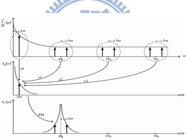
flat region and a 1 / f region, as shown in Fig. 1 - 9, [33]. Equation (1.6) shows that noise
components located near integer multiples of the oscillation frequency are weighted by Fourier coefficients of the ISF and integrated to form the low noise frequency noise sidebands
for S( ) . These sidebands in turn become close-in phase noise in the spectrum of Sv( )
through phase modulation (PM), as shown in Fig. 1 - 9. The definition of the ISF can be expanded to take into account the presence of cyclostationary noise sources such as the channel noise of a MOS transistor. Its statistical properties vary with time in a periodic manner because the noise power is modulated by the gate-source overdrive voltage.
Fig. 1 - 9 Conversion of circuit noise to excess phase, and then to phase-noise sideband
Now consider with a white input noise current with power spectral density 2
/
n
i f . Note
that I in equation (1.11) represents the peak and not the rms amplitude, hence, n
2 2
/ 2 /
n n
equal sidebands at O , as shown in Fig. 1 - 8. However, it is important to recognize that
noise power at nO also has a similar effect. Therefore, twice the power of noise at
O
n should be taken into account, and hence equation (1.11) becomes
2 2 2 0 1 2 2 max 2 ( ) 10 log 8 n n n i c c f L q
(1. 12)According to Parseval's relation,
2 2 2 2 0 2 1 0 1 2 ( ) 2 rms n n c x dx c
(1. 13)where rmsis the rms value of ( )x . As a result equation (1.12) becomes
2 2 2 2 max ( ) 10 log 2 n rms i f L q (1. 14)
This equation gives the phase noise spectrum of an arbitrary oscillator in the 1 / f region of 2
the phase noise spectrum.
Many active and passive devices exhibits low frequency noise with a power spectrum that is approximately inversely proportional to the frequency. It is for this reason that noise
source with this behavior are referred to as 1 / f noise. Noting that device noise in the 1 / f
region can be described by
in2,1/f in2 1/f
where 1/ f is the corner frequency of device 1 / f noise. Hence, the sideband power
relative to the carrier in the 1 / f portion of the phase noise spectrum can be expressed as 3
2 1/ 2 0 2 2 max ( ) 10 log 8 f n i c f L q (1. 16)
The phase noise 1 / f corner, 3 1/ f3, is the frequency where the sideband power due to the
white noise given by equation (1.14) is equal to the sideband power arising from the 1 / f
noise given by equation (1.16), as shown in Fig. 1 - 10.
Fig. 1 - 10 S( ) on a log-log axis, [33]
Solving for 1/ f3 resulting in the following expression for the
3
1 / f corner in the phase noise spectrum:
3 2 0 1/ 1/f f rms c (1. 17)
As can be seen, the 1 / f phase noise corner is not equal to the 3 1 / f device noise corner
but smaller by a factor equal to
2 0 rms c
, where c is the dc value of ISF, 0
2 0 0 1 ( ) 2 c x dx
(1. 18)Therefore, if the circuit can be designed such that the ISF corresponding to each transistor noise source has no DC component, the flicker noise will not have any effect on the phase noise of the VCO.
A white cyclostationary noise current can always be decomposed as
i tn( )in0( )t ( Ot) (1.19)
where in0( )t is a white stationary process and ( Ot) is a deterministic periodic function
describing the noise amplitude modulation and therefore is referred to as the noise modulating function (NMF). The NMF is normalized to a maximal value of one and can be easily derived from the device noise characteristics and noiseless steady-state waveform. Therefore, the expression for the excess phase resulting from a cyclostationary noise source can be written as
0
max ( ) t O O n t t i d q
(1. 20)As can be seen, cyclostationary noise can be treated as a stationary noise applied to a system
with a new ISF given byNMF( )x ( )x ( )x where ( Ot) can be derived easily from
device noise characteristics and the noiseless steady-state waveform.
In summary, the linear time-variant phase-noise model proposed by Hajimiri and Lee can ( )
n
accurately predict phase noise of most practical oscillators by taking into account the cyclostationary properties of the random noise sources. The introduced ISF accurately describes the contribution to phase perturbation by each individual noise source, allowing efficient optimization of phase noise performance.
1.3
Thesis Organization
In this thesis, a Colpitts current-reused quadrature VCO on capacitor coupling and a high gain down conversion mixer are implemented in TSMC 0.18 μm mixed-signal/RF CMOS 1P6M technology.
Chapter 1 discusses the background of low phase noise CMOS QVCO and high gain mixer , and gives a brief introduction to phase noise.
Chapter 2 presents a quadrature VCO on capacitor coupling which combine current-reused oscillator with Colpitts structure. This method is able to exist low phase noise and generate quadrature signals. Compared with conventional P-QVCO, it doesn't trade off phase noise and phase error. Furthermore, using capacitor coupling to generate quadrature signals doesn't make extra phase noise.
Chapter 3 will propose a high gain down conversion mixer. The proposed mixer with current bleeding circuit constructs common mode feedback (CMFB) circuit in active load and CS-LNA in RF trans-conductance stage. Besides, the inductor connecting with switch pairs can reduce indirect noise. By these methods, the propose mixer can achieve high conversion gain at low noise figure easily.
Chapter 4 presents a broadband high gain down conversion mixer with cascade structure. The cascade structure in RF trans-conductance stage combines CS-LNA with capacitor cross-coupled CG-LNA (CCC CG-LNA). Compared with the traditional CG-LNA in cascade structure, the CCC CG-LNA not only matches input impedance widely but also improves the performance of noise figure and the effective trans-conductance that is almost twice as large as general CG-LNA. Hence, the proposed mixer can achieve high conversion gain and low noise figure in broadband.
Chapter 2
A Colpitts Current-Reused QVCO Based on Capacitor
Coupling
2.1
Introduction
Modern RF receivers and transmitters require oscillators with accurate phase and low phase noise. Since most of the current wireless communication systems are employing quadrature modulation, there have been various research to obtain accurate quadrature local oscillator (LO) signals with low phase noise. For quadrature signals, in-phase and quadrature-phase (I/Q) match is an important requirement while meeting the requirements of low-phase noise and low power consumption for integrated VCOs. Coupling two differential VCOs to generate quadrature signals is called quadrature coupling technology, as shown in Fig. 2 - 1, and is widely used because of its better phase noise. So, we use the quadrature coupling method to generate the quadrature signals in this chapter.
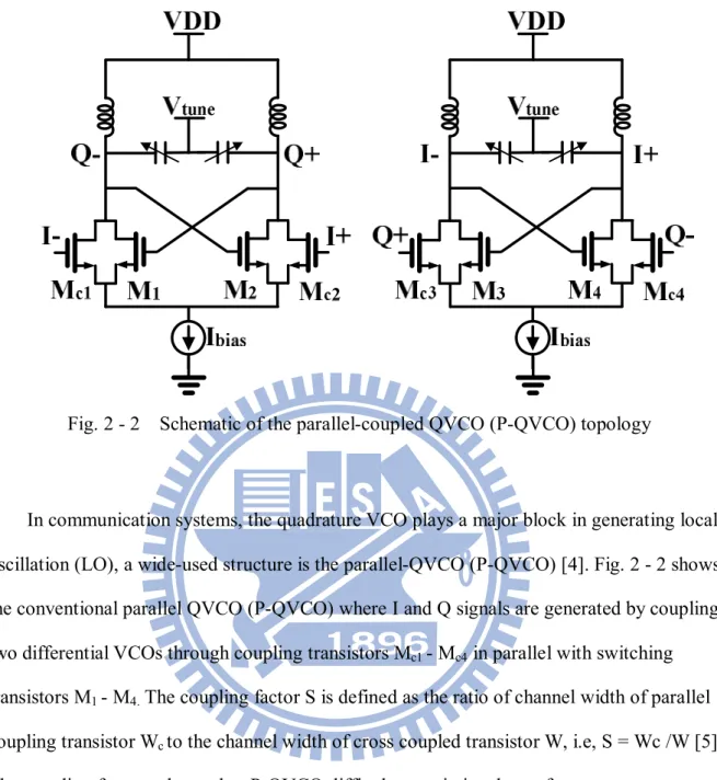
Fig. 2 - 2 Schematic of the parallel-coupled QVCO (P-QVCO) topology
In communication systems, the quadrature VCO plays a major block in generating local oscillation (LO), a wide-used structure is the parallel-QVCO (P-QVCO) [4]. Fig. 2 - 2 shows the conventional parallel QVCO (P-QVCO) where I and Q signals are generated by coupling
two differential VCOs through coupling transistors Mc1 - Mc4 in parallel with switching
transistors M1 - M4. The coupling factor S is defined as the ratio of channel width of parallel
coupling transistor Wc to the channel width of cross coupled transistor W, i.e, S = Wc /W [5].
The coupling factor value makes P-QVCO difficult to optimize the performance parameters like phase noise and phase accuracy. It means the P-QVCO suffers from a trade-off between phase noise and phase accuracy. The phase noise degradation is induced by the increase in transconductance of the coupling transistors. In addition, the increase in S leads to a higher amount of power dissipation.
In order to achieve low power consumption, current-reused VCO (CR-VCO) configuration is one of the most widely used solutions. Fig. 2 - 3 shows the schematic of the conventional NMOS-based current-reused VCO (CR-VCO) by stacking switching transistors in series like a cascode [6].
Fig. 2 - 3 Schematic of the conventional current-reused topology
Unfortunately, there are three drawbacks of this type CR-VCO. First, compared with the general VCO, the frequency tuning range of this type CR-VCO is narrower. Because the DC
levels at the two sides of the varactors are different, the capacitors Cblk must be added for dc
block and ac short to have the identical voltage drop across the varactors. Besides, the
capacitors Ccpl and resistors Rbias should be added to bias the transistors properly. Therefore,
the capacitance tuning range Cmax / Cmin will be smaller due to the addition of extra capacitors.
Involving too large number of capacitors and higher capacitive load at the output node also
attached at the node X. Because the node X is pulled up when each one of the differential NMOS turns on, the frequency at the node X is twice as the frequency at the VCO output. A
large capacitor Cgnd should be used to have a tight ground effect, symmetric differential output
swing and suppress the high frequency noise at node X. Third, the amplitude imbalance of the output signals is relatively larger than the conventional cross-coupled VCO due to the unsymmetric circuit structure.
Fig. 2 - 4 Schematic of another conventional current-reused topology
Another type of CR-QVCO has been reported in [7], as shown in Fig. 2 - 4. This structure exists three advantages, low phase noise、half power consumption of standard LC-VCO and easily start-up oscillation. This technology replaces one NMOS in conventional cross-coupled pair by PMOS. Using PMOS transistors in the cross-coupled pair can additionally reduce the phase noise due to lower flicker noise and hot carrier effects. And the series stacking of NMOS and PMOS allows the current to be reduced about half of standard VCO. Also, it is easy to
topology is much easier than the NMOS-based cascode current-reused VCO (CR-VCO) topology. That is, the DC levels at the two sides of the varactors are the same and no extra capacitors are needed. Therefore, the problem of involving large number of capacitors and higher capacitive load at the output node can be solved.
Although the CR-QVCO using the configuration shown in Fig. 2 - 4 has excellent low power consumption, there is a drawback that the amplitude imbalance of the output signals is relatively larger than the conventional cross-coupled VCO due to the asymmetric circuit structure. To solve this problem, a passive degenerative resistor is added at the source node of the NMOS transistor to balance the different trans-conductance between PMOS and NMOS transistor.
Fig. 2 – 5 Schematic of Colpitts VCO topology
Fig. 2 - 5 is shown Schematic of Colpitts VCO topology. According to Colpitts technology, it shows a better phase noise performance due to large output voltage swing and better cyclostationary noise property [5]. However, the drawback of Colpitts is hard to oscillate because the transistor of Colpitts must need high gain to start up oscillator.
2.2
Circuit Design Consideration
The circuit was simulated and optimized using Agilent ADS. The design procedure can be divided in two steps. First, it analyses the parameters of inductor and chooses the optimal inductor. Finally, a large signal analysis was performed with the harmonic balance to simulate the performance of proposed circuit and output power of the fundamental signal as well as the
harmonic signals. In the 1 f region, the phase noise is given as [8] : 2
2 2 , 2 2 2 max 1 8 n off rms n n off i L f f q f
(2.1)where foff is the offset frequency from the carrier and qmax CVtank Vtank (Ltank
2osc) isthe total charge swing of the tank. The impulse sensitivity function (ISF), , represents the
time-varying sensitivity of the oscillator’s phase to perturbations. Equation (2.1) can be easily
interpreted by Vtank Ibias Gtank Ibias GL, GL is the conductance of inductor. Setting to
oscillation frequency fosc and DC current Ibias, equation(2.1) will be used define a design
strategy [8] :
off
tank L
2L f L G
(2.2)
Fig. 2 - 6 to Fig. 2 - 7 show the performance of the inductor that be implemented in
TSMC 0.18 μm mixed-signal/RF CMOS 1P6M process. Using the data of Fig. 2 - 6, it can be
seen the factor
Ltan kGL
2 in equation (2.2) increasing with an enhancing inductance.However, it needs more DC power to compensate the loss of tank if we choose minimum inductance to achieve better phase noise, as shown Fig. 2 - 7. So, it is important to choose optimal inductor from Fig. 2 - 6 to Fig. 2 - 7.
Fig. 2 – 6 The equation (2.2) of inductor
Fig. 2 – 7 The inductance and conductance of inductor
Fig. 2 - 2 shows a schematic of the P-QVCO which is proposed by [4]. In general, the QVCO consists of the two VCO cores and these two VCOs cores are connected through
active device. This structure uses coupling transistors Mc1~Mc4 which are parallel with
cross-coupled transistors M1~M4 to generate quadrature signals. However, compared with a
more than twice power of the standard VCO but also exhibit poor phase noise due to the
additional components Mc1~Mc4.
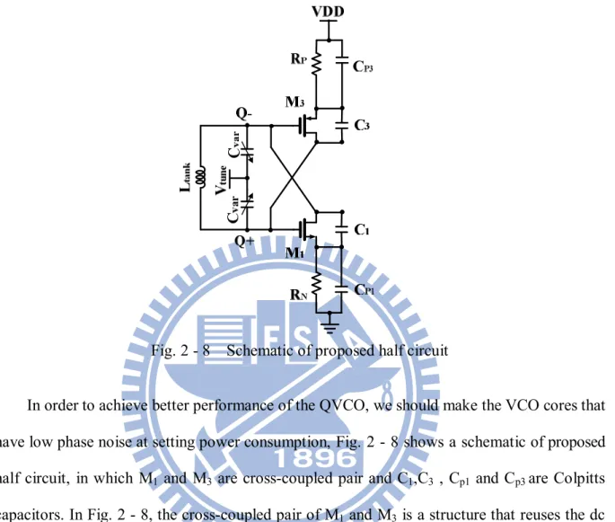
Fig. 2 - 8 Schematic of proposed half circuit
In order to achieve better performance of the QVCO, we should make the VCO cores that have low phase noise at setting power consumption, Fig. 2 - 8 shows a schematic of proposed
half circuit, in which M1 and M3 are cross-coupled pair and C1,C3 , Cp1 and Cp3 are Colpitts
capacitors. In Fig. 2 - 8, the cross-coupled pair of M1 and M3 is a structure that reuses the dc
current so that only consumes the half power of a standard VCO. Besides, this proposed VCO
exhibits a better phase noise than standard VCO because PMOS (M3) in complementary
cross-coupled pair owns lower flicker noise and hot carrier effects [7]. However, the amplitudes of oscillation signals are asymmetric due to the trans-conductance of PMOS and
NMOS are mismatch. In order to solve this problem, the source degeneration resistances RN,
RP used to balance voltage swings. Beside, these resistances control the DC current and lead
current-reused VCOs into current-limited region [7]. The proposed VCO is used to design QVCO in this chapter. This structure can get the advantages of current-reused VCO. Besides, combining Colpitts technology with current-reused structure also makes better phase noise.
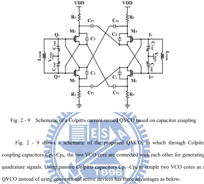
Fig. 2 - 9 Schematic of a Colpitts current-reused QVCO based on capacitor coupling
Fig. 2 - 9 shows a schematic of the proposed QVCO, in which through Colpitts
coupling capacitors Cp1~Cp4, the two VCO core are connected with each other for generating
quadrature signals. Using passive Colpitts capacitors Cp1~Cp4 to couple two VCO cores as a
QVCO instead of using conventional active devices has three advantages as below: (1) This capacitor coupling method can reduce the power consumption.
(2) It can improve phase noise performance.
(3) It doesn’t consider the trade-off of phase noise and phase accuracy.
The first is that the additional power consumed by active device such as Mc1~Mc4 in
P-QVCO can be removed. So, it can reduce the power consumption of proposed QVCO by capacitor coupling method. The second is to avoid phase noise degradation because the
passive devices are noiseless. The third is that the active coupling transistors Mc1~Mc4 make
P-QVCO difficult to optimize phase noise and phase accuracy. The technique using capacitor to generate quadrature signals doesn’t consider the coupling factor that defines as traditional P-QVCO.
2.3
Chip Layout and Simulation Results
Fig. 2 - 10 shows the chip layout photograph of the proposed QVCO which is implemented in TSMC 0.18 μm mixed-signal/RF CMOS 1P6M process. The chip size is 1 ×
0.78 mm2 including all pads and bypass capacitances. Each buffer of the QVCO output is
designed as a common-source amplifier with bias-tee model. The core power consumption is 6.462 mW at 1.8 V supply.
Compared with P-QVCO, as shown Fig. 2 - 2, the proposed QVCO has three advantages: (1) Low phase noise
(2) It doesn’t consider the trade-off of phase noise and phase error. (3) Reducing power consumption.
The first combines current-reused VCO with Colpitts structure. And also it makes better phase noise by passive device coupling than active devise. Second, the active coupling transistors
Mc1 to Mc4 make P-QVCO difficult to optimize phase noise and phase error. Using capacitor
to generate quadrature signals doesn’t consider the coupling factor that defines as traditional P-QVCO. Finally, proposed QVCO only uses two branch currents to get desired trans-conductance. However, P-QVCO needs four branch currents to get same trans-conductance.
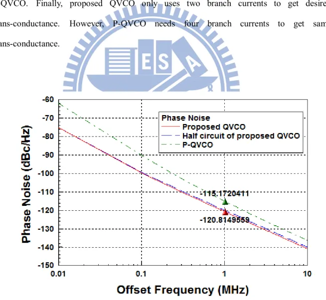
Fig. 2 - 11 shows the pre-simulated phase noise performances of proposed QVCO, a stand-alone VCO of Fig. 2 - 6 and the P-QVCO of Fig. 2 - 2. Under supplied voltage of 1.8 V for all simulations at 5 GHz, the power consumption of the proposed QVCO is equal to the P-QVCO and is twice of the stand-alone VCO. In Fig. 2 - 11, the phase noise at 1MHz offset frequency of proposed QVCO is quite close to that of the stand-alone VCO. Compared with the phase noise of P-QVCO, the phase noise of proposed QVCO is better about 5 dB. Consequently, using Colpitts capacitor to couple quadrature signals doesn’t make extra phase noise.
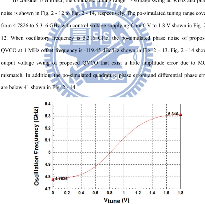
To consider EM effect, the simulated tuning range 、voltage swing at 5GHz and phase noise is shown in Fig. 2 - 12 to Fig. 2 - 14, respectively. The po-simulated tuning range covers from 4.7826 to 5.316 GHz with control voltage supplying from 0 V to 1.8 V shown in Fig. 2 - 12. When oscillatory frequency is 5.316 GHz, the po-simulated phase noise of proposed QVCO at 1 MHz offset frequency is -119.45 dBc/Hz shown in Fig. 2 – 13. Fig. 2 - 14 shows output voltage swing of proposed QVCO that exist a little amplitude error due to MOS mismatch. In addition, the po-simulated quadrature phase errors and differential phase error are below 4° shown in Fig. 2 - 14.
Fig. 2 - 13 Simulated phase noise of the proposed QVCO
2.4
Measurement Results and Comparison
2.4.1 Measurement Consideration
The proposed QVCO are designed for on-wafer testing, and the DC voltage are supplied by two sets of three-pin probe, so that the distance between each DC pad is 100um to satisfy the probe testing rules. The output buffer of each quadrature output is designed using common-source amplifier, and the drain end of each buffer is connected to the RF pad. For measurement, we connect four bias-tee terminals to the corresponding RF pads.
The phase noise, tuning range and output spectrum are measured by signal source analyzer (Agilent E5052B) shown in Fig. 2 - 15. The output voltage swing is measured by digital signal analyzer (Agilent DSA91204A) shown in Fig. 2 - 16.
Fig. 2 - 16 Digital Signal Analyzer (Agilent DSA91204A)
The Chip photo of the proposed QVCO is shown in Fig. 2 - 17. Fig. 2 - 18 shows the arrangement of DC and RF probes. The core DC consumption is 8.46 mW with 1.8 V. The measured phase noise at 1 MHz、output spectrum、output swings and tuning range, was shown in Fig. 2 - 19 to Fig. 2 - 22, respectively. When oscillatory frequency is 5 GHz, the measured phase noise of proposed QVCO at 1 MHz offset frequency is -119 dBc/Hz shown in Fig. 2 - 19. As shown in Fig. 2 - 20, the output power at 5 GHz is -8 dBm without compensating buffer effect and the loss of coaxial cables line. Measured output swings are shown in Fig. 2 - 21. According to measured swings data, the average phase error of quadrature signals and different signals is 8° and 9° respectively. The measured tuning range covers from 4.57 GHz to 5.02 GHz with control voltage supplying from 0 V to 1.8 V shown in Fig. 2- 22.
Fig. 2 - 19 Measured phase noise of the proposed QVCO
Fig. 2 - 20 Measured output spectrum of the proposed QVCO
Fig. 2 -22 Measured tuning range of the proposed QVCO
The figure of merits (FOM) for oscillators summarizes the important performance parameters, i.e., phase noise and power consumption , to make a fair comparison is defined in [40] as :
20log
10log(
)
1
OP
DCFOM
L
mW
(2.3)where ∆f is offset frequency, L
is phase noise at offset frequency, is the Ooscillation frequency, P is the power consumption of core circuit. Table 2 - 1 summarizes DC
the simulated and measured results of the proposed QVCO. Every measured performance is close to simulated results except frequency range. Table 2 - 2 shows the comparison of the measured results of proposed QVCO with the published papers of QVCOs. From Table 2 - 2, it can get proposed QVCO making better performance than other QVCO at same frequency and process
Table 2 - 1 Simulated results of the proposed QVCO
Po-simulation Measurement
Process TSMC 0.18um CMOS
Tuning Range (GHz) 4.7826 - 5.316 4.57 - 5.023 Bandwidth (MHz) 533.4 453 PhaseNoise@1MHz (dBc/Hz) -119.45 -119 Output Power (dBm) -5.9 -8 Supply Voltage (V) 1.8 1.8 Core Power (mW) 8.586 8.46 FOM -184.04 -183.6
Table 2 - 2 Comparison of QVCO performance
Process Tuning Range Phase Noise @1MHz Supply Voltage Core Power FOM This work (Chapter 2) 0.18μm CMOS 4.57-5.02 GHz -119 dBc/Hz 1.8V 8.46mW -183.7 [9] MWCL, 2009 0.18μm CMOS 4.39-5.26 GHz -113.65 dBc/Hz 1.8V 6.3mW -180.0 [10] MWCL, 2005 0.18μm CMOS 5.50-6.70 GHz -115 dBc/Hz 1.8V 1.84mW -182.2 [11] RFIC, 2002 0.18μm CMOS 6/9 GHz -106 dBc/Hz 1.8V 6.8mW -173.2 [12] PIERS 2007 0.18μm CMOS 5.15-5.75 GHz -107 dBc/Hz 1.8V 1.5mW -177 [13] EDSSC, 2007 0.18μm CMOS 5.25-5.58 GHz -113 dBc/Hz 1.8V 21.6mW -174.6
Chapter 3
A High Gain Down Conversion Mixer in Ku Band
3.1
Introduction
Mixer is an essential component of an RF system and translates the IF signal to a carrier frequency for transmission. Mixer operates either the trans-conductance of an amplifier or the resistance of a switch to produce the mixing action through time-varying mechanism. There are many structures of active mixers (single-balanced 、 double-balanced, etc.), the double-balanced circuit have been popularly appearing in microwave and millimeter wave applications for its good isolations because it solves the problem of LO-IF feed-through from single-balanced circuit.
For example, as indicated in Fig. 3 - 1, the schematic is a typical double balanced mixer.
In order to enhance the conversion gain, it is perhaps to use large RL. However, as RL
increasing, the voltage headroom will decrease and minimize the output swing to drive next
stage hardly. Increasing the power supply VDD is a solution but it will consume more power.
Another solution is additionally current bleeding by using the two current sources as indicated in Fig. 3 - 2. Bleeding can achieve a higher conversion gain through the higher load because part of the trans-conductance stage current steers from the switching pairs. Furthermore, the transistors of switch pairs could be operated at a lower overdrive voltage and smaller size transistors could be used. In either case, for setting power of local signal, bleeding improves the conversion efficiency when lower charges are necessary to turn them on and off. However, bleeding degrades at high frequency performance of the trans-conductance stage due to the higher impedance at the output as the smaller DC currents through the switching pairs reduce their trans-conductance [14].
3.2
Circuit Design Consideration
The proposed high gain mixer is shown in Fig. 3 - 3. It can be divided mixer into three blocks, active load, switch pairs and radio frequency (RF) trans-conductance stage like Fig. 3 - 4 and discuss each block respectively.
Fig. 3 - 3 The proposed high gain mixer
The active load is shown Fig. 3 - 5. The transistors M9 and M10 are the active load of the
mixer replacing passive load resistors of conventional mixer. Furthermore, using M9 、M10
and RL to construct common mode feedback circuit (CMFB) can stabilize the IF ports (IF+、
IF- ) and restrain the common mode signal from the IF ports. RL also can prevent the IF ports
dropping as it is increased to provide more conversion gain. This will provide a better linearity than passive load structure even if the conversion gain is increased [27].
Fig. 3 - 5 The active load by CMFB circuit
The switching pairs are formed by four transistors M5-M8 and the current-bleeding
circuit is composed of transistors M11-M12, shown Fig. 3 - 6. The current-bleeding circuit [14]
plays an important component in the operation of the down-conversion mixer. First, it improves the conversion gain. Second, the switching pairs can be biased with a low overdrive voltage that reduces the local signal power needed for switching and makes the switching more ideal [14].
Fig. 3 - 7 The LNA trans-conductors for mixer
The LNA trans-conductors with inductor Lsis used to design RF trans-conductance stage
[16] shown in Fig. 3 - 7. It is used the LC match input T-model network to simulate optimal noise and impedance matching. This match method yields good input matching and achieves minimum noise figure at the same time easily. Optimum the fingers of transistors and gate bias voltage are needed to get a minimum noise figure for the LNA. But, in mixer, the flicker noise of the switching pairs translates to output due to the direct and indirect mechanism that is explained in [15]. To minimize the noise effect of the direct mechanism, the current-bleeding circuit is used to decrease the dc current through the switch pairs. However, the current-bleeding circuit also adds noise to mixer. To minimize the noise of the current-bleeding circuit, PMOS transistor is chosen and biased at the optimum overdrive voltage for minimum noise. The size of switch transistors increases for getting high conversion gain as soon as tail capacitances of the switching pairs increase. It results extra flicker noise translating to the output indirectly [25]. This phenomenon is called noise in
indirect mechanism. If parallel inductor L1 be used to resonate out the tail-capacitance, the
3.3
Simulated and Measured Results
The proposed high gain mixer is simulated and optimized using Agilent ADS. Fig. 3 - 8 shows the chip layout of the proposed high gain mixer which is implemented in TSMC 0.18
μm mixed-signal/RF CMOS 1P6M process. The mixer size is 0.7 × 1.4 mm2 including all
pads and bypass capacitances. Each buffer of the IF ports were designed as a common-source amplifier.
Fig. 3 - 9 The full chip photograph of integrated circuit
Fig. 3 - 9 shows the chip photograph of integrated circuit that includes antenna (0.7 × 1.4
mm2) and high gain mixer (0.7 × 1.4 mm2). Fig. 3 - 10 shows the simulated and measured
s-parameter of RF ports. The simulated result without antenna is an exact performance of proposed mixer. However, it cannot cut the antenna to get the true results of mixer when the probe contacts the pad of mixer to measure performance. So, the matching s-parameter of mixer shifts to high frequency because the load of antenna affects matching impendence that smaller than standard impendence during measurement. As shown Fig. 3 - 10, the simulated s-parameter without antenna is below -10 dB in 12.5~15 GHz and with antenna is below -10 dB in 13~20 GHz. The measured s-parameter is averagely below -10 dB in 6~20 GHz.
Fig. 3 - 11 shows the simulated and measured the bandwidth of conversion gain while radio frequency down converts to 100 MHz. The simulated result with antenna or not exhibits the 3 dB gain bandwidth from 11.5 to 14.8 GHz and the maximum conversion gain is 22.285 dB at 13 GHz. However, the measured result decreases 4 dB approximately. The maximum conversion gain is 18.3 dB at 14 GHz and bandwidth covers from 12 to 16 GHz. As shown Fig. 3 - 12, the simulated noise figure without antenna is below 9 dB in 12~15.5 GHz and with antenna is below 12.3 dB in 12~16 GHz. The measured noise figure is below 16 dB in 12~16 GHz and the minimum is 13.214 dB at 13.5 GHz.
Fig. 3 - 10 The input return loss of the proposed high gain mixer
Fig. 3 - 12 The noise figure of the proposed high gain mixer
Fig. 3 -13 and Fig. 3 - 14 show the simulated and measured linearity at 14 GHz that is the radio frequency of the maximum conversion gain. The simulated linearity shows that P1dB is -26 dB and IIP3 is -15 dB. The measured linearity shows that P1dB is -16 dB and IIP3 is -7.5 dB. Fig. 3 -15 shows the measured isolation from 9.9 to 18 GHz. The LO-IF isolation is below -35 dB, the LO-RF isolation is below -55 dB and the RF-IF isolation is below -35 dB. The figure of merits (FOM) for mixer summarizes the important performance parameters and formula is defined as:
FOM
Mixer=
20log(
f
RF)+
CG NF DSB
(
)
IIP
3 10log(
P
Consumption)
(3.1)where fRF is the center frequency. CG is the conversion gain. NF DSB( ) is noise figure at
double-side band. IIP3 is input third-order intercept point. PConsumptionis power consumption.
Table 3 - 1 summarizes the simulated and measured results of the proposed high gain mixer. The simulated FOM is 193.7 by equation (3.1). However, the measured FOM drops to 191.42.
Including the antenna load effect, the simulated power consumption is not equal to the measured power consumption. This condition must be process variation. Also, the proposed mixer is used by idea balun to generate different signals and drive proposed mixer. The performance of idea balun is obviously different from the real balun that used in measurement because real balun exists phase error but idea balun doesn’t. So, from Fig. 3 – 11 to Fig. 3 – 15, the simulated results are not fit measured results perfectly due to process variation and using real balun.
Fig. 3 - 13 The P1dB of the proposed high gain mixer
(b) Measurement
Fig. 3 - 14 The IIP3 of the proposed high gain mixer
Table 3 -1 Simulated results of the proposed high gain mixer
Simulation Measurement
Technology TSMC 0.18um CMOS
RF Freq. 11.5~14.8 GHz 12~16 GHz IF Freq. 100 MHz 100 MHz LO Power 0 dB 0 dB Conversion Gain,max 22.285 dB 18.327 NF 8~9 13.2~15.9 P1dB -26 dB -16 dB IIP3 -15 dB -7.5 dB LO-to-RF isolation < -40 dB < -55 dB LO-to-IF isolation < -35 dB < -35 dB RF-to-IF isolation < -35 dB < -35 dB Power Consumption 6.12 mW 7.56 mW FOM 193.7 191.42
Table 3 -2 Comparison of mixer performance This Work (Chapter 3) [27] [28] [29] [30] Process TSMC 0.18 um CMOS TSMC 0.18 um CMOS 0.18um CMOS 0.18um CMOS TSMC 0.18 um CMOS RF Bandwidth(G Hz) 12 ~15 12~18 6 ~9 6 ~10 5.725~5.825 Conversion Gain (dB) 15.3~18.3 6.52~8.12 14~14.8 8 11.06 Noise Figure (dB) 13.2~15.9 17.26 15.1 13.5 12.8 P1dB (dB) -16 NA NA NA -16.4 IIP3 (dB) -7.5 3.5 -13.9 NA -7.5 Power Consumption (mW) 7.56 6.36 17.4 10.5 3.6 FOM 191.42 189.84 170.9 182.34+ NA 180.43
Chapter 4
4-17 GHz Wideband High Gain Down
Conversion Mixer with Cascade Structure
4.1
Introduction
Direct conversion front-end circuit is a very important component in wireless communication system. Generally, front-end circuit must be constituted by low-noise amplifier (LNA) and mixer. The mixer is a key block to translate signals in the system. In the development of modern wireless applications, wideband frequency range, low power consumption and small chip area are the aims of work. For these topics, the idea of high gain mixer is proposed and replaced conventional front-end circuit further. The double-balance mixer is commonly used because the advantage of this active mixer is good isolation [14]. However, the main challenge in double-balanced mixer is to decrease noise figure and extend frequency range for more applications at steady high conversion gain.
In this chapter, a broadband high gain mixer is presented for many bands applications such as C band (4~8 GHz)、X band (8~12 GHz) and most part of ultra-wide band (3.1~10.6 GHz) and Ku band (12~18 GHz). The RF trans-conductance stage of proposed mixer uses cascade structure that the capacitor cross-coupled wideband amplifier at first stage replaces passive LC input match network to design high gain mixer at wide frequency range.
4.2
Circuit Design Consideration
Radio frequency designs are increasingly used in advance CMOS process that makes the integration of complete communications systems possibly [17]. The proposed mixer at this chapter is shown in Fig. 4 – 1. In high gain mixer, the blocks of active load and switch pair are discussed at chapter 3. This section focuses on RF trans-conductance stage how to achieve high gain and low noise figure in wideband. The RF part can be divided into CS-LNA [17] at second stage and CCC CG-LNA [20] at first stage.
![Fig. 1 - 1 The diagram of downlink [1]](https://thumb-ap.123doks.com/thumbv2/9libinfo/8734526.202469/14.892.258.707.459.800/fig-diagram-downlink.webp)
![Fig. 1 - 4 A typical phase noise plot for a free running oscillator, [33]](https://thumb-ap.123doks.com/thumbv2/9libinfo/8734526.202469/17.892.138.797.503.974/fig-typical-phase-noise-plot-free-running-oscillator.webp)
![Fig. 1 - 6 The equivalent system for ISF decomposition, [33]](https://thumb-ap.123doks.com/thumbv2/9libinfo/8734526.202469/20.892.133.811.255.771/fig-equivalent-isf-decomposition.webp)
![Fig. 2 - 5 is shown Schematic of Colpitts VCO topology. According to Colpitts technology, it shows a better phase noise performance due to large output voltage swing and better cyclostationary noise property [5]](https://thumb-ap.123doks.com/thumbv2/9libinfo/8734526.202469/33.892.265.622.471.887/schematic-colpitts-according-colpitts-technology-performance-cyclostationary-property.webp)