USING Si02 NANOPARTICLES
TO EFFICIENTLY ENHANCE LIGHT EMISSION
FROM METAL-OXIDE-SILICON TUNNELING DIODES ON Si
Ching-Fuh Linl.2.3, Wu-Ping Huang2, Eih-Zhe Liang2, Ting-Wien Su2, and Hsing-Hung Hsieh’
’
Dept. of Electrical Engr., National Taiwan Univ., TaiwanGraduate Inst. Of Electro-Optical Engr., National Taiwan Univ., Taiwan Graduate Inst. Of Electronics Engr., National Taiwan Univ., Taiwan
(Email) [email protected]
ABSTRACT
Silicon dioxide nanoparticles are used as oxide layer in metal-oxide-silicon tunneling diodes. With its non-uniformity in thickness, tunneling current is concentrated in carrier accumulation region. Both electron and hole can he confined to enhance radiative recombination rate. Electroluminescence at silicon band edge (1 .Ipm) with external quantum efficiency 1.5 x lo4 has been achieved. KOH wet etch also contributes to improvement on efficiency by removing nonradiative recombination center at surface. Frequency response is exploited as tool for extraction radiative and nonradiative recombination rate.
1. INTRODUCTTON
Silicon is the most important semiconductor material for the electronics industry. However, its importance in optoelectronics is not prominent because indirect-handgap nature of Si makes it inefficient as a light source. Therefore optoelectronic integration on the silicon chip is a challenging issue. Many efforts have been devoted for decades to making silicon useful for optoelectronics. These efforts include optical waveguides [l] or micro-optics [2] on Si, as well as converting silicon into light-emitting material such porous-silicon-based devices [3-51, nanocrystalline Si [6,7], Si’-implanted Si02[8,9], deposition of polymer upon Si substrates[lO], growth of GaNupon Si suhstrates[ll,l2], and so on.
In this work we report that using Si02 nanoparticles as oxide layer in metal-oxide-silicon (MOS) tunneling diode and KOH wet etch to improve surface condition, external quantum efficiency of electroluminescence (EL)
at silicon bandgap edge (wavelength I.lpm) can be enhanced to 1 . 5 ~ 1 0 ~ . In silicon, electrons and holes cannot recombine efficiently due to momentum mismatch. To overcome this difficulty, we use Si02 nanoparticles to generate nano-structural confinement of electrons and holes. Traditional oxide layer is replaced by Si02 nanoparticles (particle size 8-12nm) [13]. With its non-uniformity in oxide thickness, two major effects take place. First, in n-type silicon, holes tunneling through thin region of oxide layer are orders of magnitudes more than those through thick region and this leads to concentration of injected minority carriers (holes). Second, band bending toward the Si/Si02 interface also depends on oxide thickness. This leads to local concentration of accumulated majority carriers (electrons). As a result, excitons or electron-hole pairs are more easily formed around thin oxide region than in hulk silicon and radiative recombination rate increases.
Experiments (frequency response as well as varying efficiency) show that nano-structures in the oxide layer could enhance radiative recombination rate to comparable with Schottky-Read-Hall (SRH) nonradiative recombination rate. This indicates that nonradiative recombination is not the only dominant factor any more, and using Si02 nanoparticles can enhance silicon EL for orders of magnitude.
To further promote efficiency, KOH wet etch [14] is used to improve surface quality of silicon. In
commercially available lightly-doped silicon (lOLScm”), hulk minority lifetime can be as long as Ims. Nonradiative recombination rate is reduced to about 10’ sec-’ inside bulk silicon, which implies radiative recombination rate can be possibly larger than nonradiative one. However, nonradiative combination through surface states is still a severe problem on prohibiting light emission. Experiments show KOH wet etch can significantly increase EL intensity because KOH solution starts etch surface defects, which are centers of nonradiative recombination.
By using KOH wet etch on silicon surface and Si02 nanoparticles as oxide layer, we are able to fabricate
MOS
light emitting diodes with efficient light emission. The measured light-current (L-I) curve shows that external EL quantum efficiency rapidly increases and reaches 1.5 xIO4
for operation current hetween 2OmA to 30mA. Output power can be lOpW at injection current ofI O O m A
(or current density 12.7A/cm2). This power is measured only from periphery of top metal pad. If total EL is included, quantum efficiency should be more thanIO”. ’
2.
DEVICE
FABRICATIONThe processing steps are as follows. First, native oxide on silicon wafer is removed by buffered oxide etch (BOE) and KOH solution (45%) is subsequently applied to improve surface quality. Prepared Si02 nanoparticles
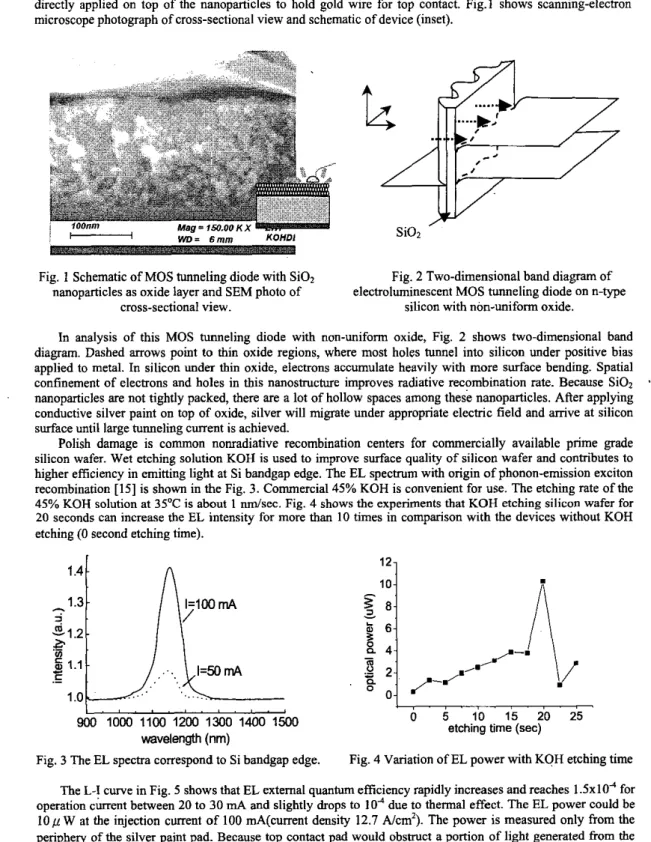
solution with feature size 8-1 1 nm is spin-coated and baked in oven. The thickness of coated oxide layer is about 150 nm. A thick layer of AI was evaporated on wafer backside to form ohmic contact. Conductive silver paint is directly applied on top of the nanoparticles to hold gold wire for top contact. Fig.] shows scanning-electron microscope photograph of cross-sectional view and schematic of device (inset).
Fig. 1 Schematic of MOS tunneling diode with Si02 nanoparticles as oxide layer and SEM photo of
cross-sectional view.
...,
b
$
+
3
...,:
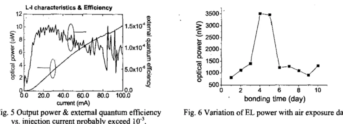
Fig. 2 Two-dimensional hand diagram of electroluminescent MOS tunneling diode on n-type
silicon with non-uniform oxide.
In analysis of this MOS tunneling diode with non-uniform oxide, Fig. 2 shows two-dimensional band diagram. Dashed arrows point to thin oxide regions, where most holes tunnel into silicon under positive bias applied to metal. In silicon under thin oxide, electrons accumulate heavily with more surface bending. Spatial confinement of electrons and holes in this nanostruchre improves radiative recombination rate. Because Si02 nanoparticles are not tightly packed, there are a lot of hollow spaces among these nanoparticles. Atter applying conductive silver paint on top of oxide, silver will migrate under appropriate electric field and arrive at silicon surface until large tunneling current is achieved.
Polish damage is common nonradiative recombination centers for commercially available prime grade silicon wafer. Wet etching solution KOH is used to improve surface quality of silicon wafer and contributes to higher efficiency in emitting light at Si bandgap edge. The EL spectrum with origin of phonon-emission exciton recombination [15] is shown in the Fig. 3. Commercial 45% KOH is convenient for use. The etching rate of the 45% KOH solution at 3S°C is about 1 &sec. Fig. 4 shows the experiments that KOH etching silicon wafer for 20 seconds can increase the EL intensity for more than 10 times in comparison with the devices without KOH etching (0 second etching time).
,
900 1000 1100 1200 1300 1400 1500 wavelength (nm)
b
5 10 15 20 25etching time (sec)
Fig. 3 The EL spectra correspond to Si bandgap edge. Fig. 4 Variation of EL power with KOH etching time The L-I curve in Fig. 5 shows that EL extemal quantum efficiency rapidly increases and reaches 1 . 5 ~ 1 0 ~ for operation current between 20 to 30 mA and slightly drops to
IO4
due to thermal effect. The EL power could be 100 W at the injection current of 100 mA(current density 12.7 A/cm2). The power is measured only from the periphery of the silver paint pad. Because top contact pad would obsmct a portion of light generated from thedevice, actual light power might be more than 1 0 ~ W. If total EL power is included, quantum efficiency will reach Ld cheracierinics (L Efficiency
-
m Y 10 1.5~10'5 EF ,
v a 1.OXlO~6
5
3
8 6 Y $ 4 5 . 0 ~ 1 0 ~$
a - 8 2 a- 0.0a.
20.0 40.0 M).o Bo.o current (6)F
3000t
2000 ._E
-
1500 1000 500 0 0 2 4 6 8 10F
3000t
2000 ._E
-
1500 1000 500 0 0 2 4 6 8 10' bonding time (day)
Fig.
5
Output power & external quantum efficiency Fig. 6 Variation of EL power with air exposure days. vs. injection current probably exceedAs shown in Fig. 6, EL intensity increases for first few days and then decreases. The reason for increasing efficiency is formation of native oxide of silicon surface to passivate surface states and to prevent short contact of silver and silicon. "radiative recombination is therefore reduced. For overgrown native oxide, high electric field is needed for the same level of tunneling current. Certain region of oxide will breakdown with metal punch-th. Light efficiency reduces and resembles that of frst few days.
3. CHARACTERISTICS BY FREQUENCY RESPONSE
Frequency response uses small signal current as less-deshuctive excitation and permits measurement of carrier lifetime under low level bias condition ( < IOA/cm* ). In analysis of'carrier lifetime, both radiative and nonradiative recombination rate and its coefficient can be determined by relation between lifetime and current bias. The physical reason for lifetime-bias relation is amibuted to extension of accumulation region near surface into silicon bulk region. In EL MOSTD, light is proportional to current in static state condition. With modulated current, response time of light is limited by carrier recombination rate. To be specific, the rate equation describing minority dynamics is "p =
e
( a + B n ) p Minority carrier recombination time is definedas
r
= 1 / ( A+
Bn).
dt ed 70 60-
Y) I-
E
50 !n -I d 40 300 1 2 3 4 5 6 7 8 9 10Bias wrrent density (Ah?)
Fig. 7 Measured lifetime of EL MOSTD for different fabrication condition: A, B) normal C) with KOH
removal of polish damage.
Fig. 8 Fitted recombination coefficient and theoretical recombination efficiency of EL MOSTD Fig. 7 shows the relation between measured lifetime from frequency response and bias current. Device A and B are MOSTLI fabricated by application of 120nm thick layer of SiOz nanoparticle. Device C is fabricated in the same way except being pre-treated with KOH wet etch. All devices have metal pad area O.O1cmz. The
external light emission efficiency qat is 5x10⁴, 2x10' and 10' (W/A) respectively. With the same light extraction efficiency q. and minority carrier injection efficiency qbi, internal or radiative recombination efficiency q- is proportional to external efficiency because qex,=qcqiniqmc, Devices with longer lifetime with low level bias current have better efficiency and have quite the same lifetime with high level bias current. This suggests that initially lifetime he affected by nonradiative recombination and lowering effect comes from
increasing radiative recombination by increasing carrier density.
Inverse of lifetime, or recombination coefficient z-' = A
+
Bn , under certain level of injection current density J, reveals simple relation with camer density n. However, it lacks theoretical explanation of complex relation between n and J. Observation in Fig. 8 allows us to empirically approach n-J relation. byn yJ' .This saturation behavior of carrier density comes from physical consideration that increasing injection current at high level only extends accumulation depth rather than increases n. Carrier lifetime is related to injection current density by;' = A + B ~ I
-
~ f l *
as shown by solid line in Fig. 8.This measurement fitting permits identification of individual conhihution of radiative and nonradiative recombination rate. Fitted A is 17185 (sec.'), Be is 320 (sec-'A-'cm2) and By is 0.718 (sec-'A-'cm2). However, only nonradiative recombination coefficient can be independently extracted. With typical value of B coefficient as 10~15cm3/sec [6], majority carrier density n is in order of 1019-1020cm-3.
Ratio of radiative recombination rate to overall recombination rate, or radiative recombination efficiency I ~ ~ ~ = B ~ I ( A + B ~ ) can be obtained, as shown by dash line in Fig. 8 . This ratio reaches more than 50% at injection current density 5Ncm2, indicating that radiative recombination is more efficient than nonradiative recombination. This high recombination efficiency comes from selection of high quality silicon wafer for fabrication of EL MOSTD and using SiOz nanoparticles to provide improved carrier confinement to increase carrier density. Although intemal efficiency is high, external efficiency is limited by low light extraction efficiency due to metal pad and low minority injection efficiency.
With kequency response analysis of radiative and nonradiative recombination rate, it is confirmed that intemal efficiency of our light emitting diode is very high.
4. CONCLUSION
We have demonstrated that use of Si02 nanopasticles and KOH wet etch can improve electroluminescence of MOS tunneling diode based on silicon. The possibility of efficient EL from MOS tunneling diodes gives great promise on integrated optoelectronics of silicon.
REFERENCES
[I] N. Takato, K. Jinguji, M. Yasu, H. Toba and M. Kawachi
,
IEEE J. Lightwave Technol. 6, 1003 (1988) [2] M. C. Wu, L. Y. Lin, S. S. Lee and K. S . Pister, Sensors Actuactors A 50, 127 (1995)[3] L. T. Canham Appl. Phys. Lett. 57,1046 (1990)
[4] N. Koshida and H. Koyama, Appl. Phys. Lett. 60,347 (1992)
[5] S. Lazarouk, P. Jaguiro, S. Katsouba, G. Masini, S. La Monica, G. Maiello and E Ferrari, Appl. Phys. Lett. [6] S . Schuppler et al, Phys. Rev. B 52,4910.
[7] D. B. Geohegan, A. A. Puretzky, G. Duscher and S . J. Pennycook, Appl. Phys. Lett. 68,2410 (1998)
[XI
L.S .
Liao,X. M. Bao, X.
Q. Zheng,N.
S .Lo
andN.S .
Min, Appl.Phys. Lett.
68,850(1996)
[9] W. Skorupa, R. A. Yankov, I. E. Tyschenko, H. Frob, T. Bohme, m d K . Leo, App. Phys. Lett. 68,2410 [IO] D. R. Baigent, R. N. Marks, N. C. Greenham, R. H. Friends, S.C. Moratti, and A. B. Holms, Appl. Phys.
[I I ] R. Birkhahn amd A. J. Steckl, Appl. Phys. Lett. 73,1700 (1998)
[12] M. Garter, J. Scofield, R. Birkhabn and A. J. Steckl, Appl. Phys. Lett. 74, 182 (1999) [I31 C. F. Lin, P. F. Chung, M. J. Chen and W. F. Su, Optics Lett. 27,713 (2002) [I41 H. Seidel et al., J. Electrochem.
Soc.
137,3612 (1990)[15] M. J. Chen, E. Z. Liang, S. W. Cbang and C. F. Lin, J. Appl. Phys. 90,789(2001) 68 (1996)
(1996)
Lett. 65,2636 (1994)