國
立
交
通
大
學
機械工程學系
博
士
論
文
高介電常數介電質金氧金電容應用於動態記憶體與
射頻元件之研究
The Research on Metal-Insulator-Metal Capacitor Using
High-κ Dielectrics for DRAM/RF Application
研 究 生:鄭淳護
高介電常數介電質金氧金電容應用於動態記憶體與射頻元件之研究
The Research on Metal-Insulator-Metal Capacitor Using
High-κ Dielectrics for DRAM/RF Application
研 究 生:鄭淳護 Student:Chun-Hu Cheng
指導教授:周長彬、荊鳳德 Advisor:Chang-Pin Chou, Albert Chin
國 立 交 通 大 學
機械工程學系
博 士 論 文
A Dissertation
Submitted to Department of Mechanical Engineering College of Engineering
National Chiao Tung University In partial Fulfillment of the Requirements
for the Degree of Doctor of Philosophy
in
Mechanical Engineering
June 2008
高介電常數介電質金氧金電容應用於動態記憶體與射頻元件之研究
研究生:鄭淳護 指導教授:周長彬 教授
荊鳳德 教授
國立交通大學
機械工程學系
摘要
隨著超大型積體電路技術的日新月異、元件尺寸的不斷縮微,為配合現今類 比、射頻通訊和記憶體元件的發展,金氧金電容(MIM)的研發是刻不容緩的。在 各種不同的被動元件中,金氧金電容經常被廣泛的應用在射頻電路裡的阻抗匹配 與直流濾波器中﹔而且它們通常佔據了很大比例的電路面積。因此,為了有效降 低晶片的面積與成本,提高單位面積的電容值是極為需要的。為了符合未來記憶 體元件的高電容密度需求,高介電系數材料的開發似乎是唯一的選擇,但增加介 電常數和減少元件厚度所伴隨而來的高漏電,更是目前研究的主要議題之一。而 目前已開發和尚在研究的高介電常數材料包含氧化鋁(Al2O3)、氧化鉭(Ta2O5)、 氧化鋯(ZrO2)和鈦酸鍶(SrTiO3)等。 雖然,鈦酸鍶介電質(SrTiO3)具有高介電常數(κ ~50-200),但小的導帶不連續(conduction band discontinuity)和能帶寬度(bandgap),將易造成較大的漏電。 除 此 之 外 , 鈦 酸 鍶 介 電 質 必 須 要 有 結 晶 相 產 生 才 能 有 較 高 的 介 電 常 數
度(>450o C)。 因此,我們針對以上鈦酸鍶介電質所產生的問題,開發出一系列和二氧化鈦 相關(TiO2-based)的材料,其中包括了鉿化鈦氧化物(TiHfO)、鑭化鈦氧化物(TiLaO) 和鋯化鈦氧化物(TiZrO)。除了之外,我們也成功的發展出一種雙電漿處理(Dual plasma treatment)下電極的方法,我們藉由這個方法搭配這些高介電質材料,成 功的開發出高性能的金氧金電容,不但在漏電上有大幅的改善,更改良了電壓電 容 係 數 (Voltage coefficient of capacitance) 和 的 溫 度 電 容 係 數 (Temperature coefficient of capacitance)。最後,我們針對鈦酸鍶介電質進行定電壓應力測試
(constant voltage stress test),去觀察其電性和類比特性上的變化,進而推估元件 的可靠度。此一電容可靠度測試的方法將可用來作為未來金氧金電容在動態記憶 體及高頻應用上的評估。
The Research of Metal-Insulator-Metal Capacitor Using High-
κ as
Dielectrics for DRAM/RF Application
Student: Chun-Hu Cheng Advisor: Chang-Pin Chou
Albert Chin
Institute & Department of Mechanical Engineering
National Chiao Tung University
Abstract
According to International Technology Roadmap for Semiconductors (ITRS), the continuous increasing capacitance density (ε0κ/tκ) is required to scale down the device size of Metal-Insulator-Metal (MIM) capacitors that are widely used for Analog, RF and DRAM functions. To meet these requirements, the using higher κ dielectric is the only choice since the decreasing dielectric thickness (tκ) increases the
unwanted leakage current exponentially. To achieve this goal the only choice is to increase the κ value of the dielectrics, which have evolved from Al2O3, Ta2O5 (κ ~25), ZrO2 (κ ~30), to SrTiO3 (κ~50-200).
Although SrTiO3 has a large dielectric (κ ~50-200), the small conduction band
offset (-0.1eV) and bandgap to lead larger leakage current is an important issue. And
We have developed successfully a dual plasma treatment on bottom surface to reduce the growth of interracial layer and then adopted high-κ TiO2 (κ~50-80) to mix medium-κ dielectric with large conduction band offset as a dielectric to improve the electrical and analog characteristic of MIM capacitors. These TiO2-based dielectrics (κ ~40-50) such as TiHfO, TiLaO and TiZrO exhibit good performance and thermal stability. On the other hand, stress degradation is especially a concern in
low-breakdown field and small-bandgap STO materials, which also leads to high
leakage currents because of the small conduction band discontinuity (ΔΕC) with
respect to Si. Here we describe the stress behavior on electrical and analog characteristics of hi-κ MIM capacitors from low frequencies (100 kHz~1 MHz) to high frequencies (1 GHz~20 GHz). This method will be beneficial to the reliability
謝誌
這本論文能夠完成,首先要感謝的是我的指導教授 周長彬博士,老師的諄 諄教誨及做人處事的無形身教,總讓我受益良多;由衷感謝共同指導教授 荊鳳 德博士,在論文研究上,給予我耐心指導並提供我良好的研究設備及環境,老師 對於治學研究的嚴謹以及認真的態度,亦是我一生的典範。 感謝台灣積體電路製造股份有限公司(TSMC),和日本東京威力科創有限公 司(TEL),在計畫合作過程提供寶貴的建議及研究資源,讓我能順利完成此一論 文研究。在此,誠摯的感謝精密儀器中心副研究員 潘漢昌博士,總是在排除萬 難的情況下,在元件製備和材料分析上給予我最大的協助和幫忙。 感謝實驗室同儕 鄭存甫、楊學人同學,在論文研究期間,給予實驗上的建 議及協助;感謝學弟妹 黃靖謙、林士豪、蘇迺超、徐曉萱、陳維邦、周坤憶、 劉思麟。有了你們的陪伴,漫漫的博士攻讀之路不再顯得孤單,更感謝鄧志剛 同 學,在論文研究上的共同討論與分享,讓我能時時獲得新知。 最後,感謝我最親愛的父母親 鄭高洲先生與 謝金時女士,謝謝他們長久 以來的支持,在我遭遇困難與低潮,給我無盡的關懷與支持,我才能堅持至今, 完成此一博士學位. 謹以此論文獻給我最親愛的家人,謝謝你們~ 淳護 戊子年於交通大學Contents
Abstract (in Chinese)……….……….……….………i
Abstract (in English) ………..……….……….………….…iii
Acknowledgement……….……….……….………v
Contents……….……….………….……vi
Figure Captions……….……….……….…ix
Table Captions……….……….……….……xvi
Chapter 1
Introduction1.1
Motivation to study High-κ Dielectrics……….11.2
The Background of High-κ Dielectrics used for DRAM and RF Application….31.3
The Background of Metal Electrodes……….……….81.4
The Deposition method of High-κ Dielectrics……….……….101.5
The Measurement and Analysis of the MIM Capacitors……….13Chapter 2
Performance Improvement of TiHfO MIM Capacitors by Using a Dual Plasma Treatment of the Lower Electrode2.1
Introduction………..…….………172.2
Experimental procedure………..………...…………182.3
Results and discussion…………..……….…………192.4
Conclusion………..……….…..……21Chapter 3
Low Temperature Crystallized TiO2 Dielectrics for DRAM Application3.1
Introduction………….………..………..…284.4
Conclusion………...………..…32Chapter 4
Improved High-Temperature Leakage in High Density MIM Capacitors by Using a TiLaO Dielectric and an Ir Electrode4.1
Introduction………..………...………..……384.2
Experimental procedure……….…………..………..………394.3
Results and discussion………..………394.4
Conclusion………...………..…42Chapter 5
MIM Capacitors Using a High-κ TiZrO Dielectric for Analog and RF application5.1
Introduction………..………...………..……485.2
Experimental……….…………..………..………495.3
Results and discussion………..………505.4
Conclusion……….……….………..…55Chapter 6
Study on Stress Behavior of MIM Capacitors by Constant Voltage Stress7.1
Introduction………..………...………..……627.2
Experimental procedure……….…………..………..………637.3
Results and discussion………..………647.4
Conclusion……….……….………..…67Chapter 7
Using High Work Function Ni Metal to Improve the StressReliability of RF SrTiO3 MIM Capacitors
7.7
Results and discussion………..………757.8
Conclusion……….……….………..…77Chapter 8
Conclusion……….………83References……….………85
Figure Caption
Chapter 1 Introduction
Fig. 1-1
The International Technology Roadmap of SIA for Semiconductor 2006...14Fig. 1-2
Comparison of the calculated conduction band offset and experimental values for various gate oxides, by various authors……….14Fig. 1-3
Static dielectric constant versus band gap for candidate gate oxides, after Robertson………..….15Fig. 1-4
Static dielectric constant versus band gap for candidate gate oxides, after Robertson………...……15Fig. 1-5
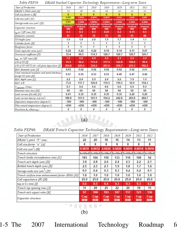
The 2007 International Technology Roadmap for Semiconductors for DRAM (a) stacked capacitors and (b) trench capacitors…………..….…16Fig. 1-6
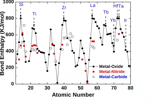
Bond enthalpy for M-O, M-N and M-C in the Periodic Table………..…17Chapter 2 Performance Improvement of TiHfO MIM Capacitors by
Using a Dual Plasma Treatment on Lower Electrode
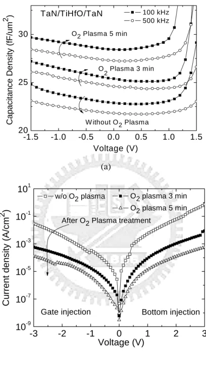
Fig. 2-1
(a) C-V and (b) J-V characteristics for TaN/TiHfO/TaN MIM capacitors measured after the indicated plasma treatments………23Fig. 3-1
Fig. 3-2
Fig. 3-3
Fig. 3-4
various plasma treatments……….………24
Fig. 2-3
Cross-sectional TEM images of the TiHfO structure (a) with only a nitrogen plasma treatment and (b) with both a nitrogen and a second oxygen plasma treatment………25Fig. 2-4
The surface roughness of bottom electrode (a) with or (b) without O2 plasma treatment by AFM spectroscopy………26Fig. 2-5
SIMS analysis for TiHfO/TaN with or without O2 plasma treatment on bottom TaN……….27Chapter 3 Low Temperature Crystallized TiO
2Dielectrics for
DRAM Application
(a) C-V and (b) J-V (measured at 25 oC and 125oC) characteristics for
Ir/TiO2/TaN capacitors……….………….34
XPS depth profile for TiO2/TaN with or without O2 treatment on bottom TaN………35 A cross-sectional TEM image of a TiO2 sample, after 300oC processing………..36 The thermal stability behavior of a 300oC –formed Ir/TiO2/TaN capacitor
Chapter 4 Improved High-Temperature Leakage in High Density
MIM Capacitors by Using a TiLaO Dielectric and an Ir
Electrode
Fig. 4-1
(a) C-V, (b) J-V and (c) thermal stability characteristics of TaN/TiLaO/TaN and TaN/Ir/TiLaO/TaN MIM capacitors measured at various frequencies, at 25oC and 125oC. The thermal stability test was performed at 400oC for20 min at N2 ambient………..45
Fig. 4-2
Measured and simulated J-E1/2 of an Ir/TiLaO/TaN capacitor. ATaN/TiLaO/TaN device is shown, for comparison, in the insert…………46
Fig. 4-3
Τhe J/T1/2-E1/2 plots of TaN/TiLaO/TaN and TaN/Ir/TiLaO/TaN MIM
capacitors………47
Chapter 5 MIM Capacitors Using a High-
κ TiZrO Dielectric for
Analog and RF Applications
Fig. 5-1
(a) C-V, (b) J-V and (c) ΔC/C-V characteristics of Al/TiZro/TaN and Ni/TiZrO/TaN MIM capacitors……….56Fig. 5-2
(a) C-V, (b) J-V and (c) ΔC/C-V characteristics of Ni/TiZrO/TaN MIM capacitors with a 47 or 56 nm TiZrO dielectric thicknesses……….58Fig. 5-3
Temperature-dependence of capacitance (TCC) characteristics of Ni/TiZrO/TaN MIM capacitors with 47 nm or 56 nm TiZrO dielectric thicknesses……….59Fig. 5-4
ΔC/C-1/C plot for various MIM capacitors………60Fig. 5-5
Thermal stability behavior of (a) C-V and (b) J-V characteristics forNi/TiZrO/TaN capacitors after a 350oC N
2 anneal for 20 min…………...61
Chapter 6 Study on Stress Behavior of MIM Capacitors by
Constant Voltage Stress
Fig. 6-1
(a) C-V and (b) J-V characteristics of the 30 nm TiHfO/TaN MIM capacitors with Ni or TaN top electrode……….68Fig. 6-2
(a) The temperature-dependent normalized capacitance and (b) ΔC/C-Vcharacteristics of TiHfO MIM capacitors with Ni or TaN top electrodes………69
Fig. 6-3
The effect of constant-voltage stress on (a) VCC-α (b) J-V and (c) TCC of [Ni or TaN]/TiHfO/TaN capacitors………71Fig. 6-4
(a) ΔC/C as a function of stress time and (b) extrapolated ΔC/C for a 10Chapter 7 Using High Work Function Ni Metal to Improve the
Stress Reliability of RF SrTiO
3MIM Capacitors
Fig. 7-1
Band diagrams before contact for (a) TaN or (b) Ni /SrTiO3/TaN MIM capacitors………..………..78Fig. 7-2
C-V characteristics of (a) [Ni or TaN]/STO/TaN at 25ºC or 125ºC and (b) J-V characteristics of [Ni or TaN]/STO/TaN under CVS test at 25ºC or125ºC………..79
Fig. 7-3
(a) Measured and simulated two-port S-parameters for SrTiO3 MIM capacitors (b) The equivalent circuit for capacitor value extraction from measured S-parameters……….…………..80Fig. 7-4
The ΔC/C of [Ni or TaN]/STO/TaN capacitors which measured (a) at 25ºCand 125ºC, (b) fresh and stressed devices and (c) stressed devices at 25ºC and
Table 3-1
Table Caption
Chapter 2 Performance Improvement of TiHfO MIM Capacitors by
Using a Dual Plasma Treatment on Lower Electrode
Table 2-1
Comparison of MIM capacitors having various dielectrics and metal electrodes………..…………22Chapter 3 Low Temperature Crystallized TiO
2Dielectrics for
DRAM Application
Comparison of MIM capacitors which have various dielectrics and metal electrodes………33
Chapter 4 Improved High-Temperature Leakage in High Density
MIM Capacitors by Using a TiLaO Dielectric and an Ir
Electrode
Table 4-1
Comparison of MIM capacitors with various dielectrics and metal electrodes………..43Chapter 5 MIM Capacitors Using a High-
κ TiZrO Dielectric for
Analog and RF Applications
Table 5-1
Comparison of MIM capacitors with various dielectrics and metal electrodes………54Chapter 1
Introduction
1.1 Motivation to Study High-
κ Dielectrics
In the scaling of CMOS devices, reducing the thickness of gate stack with lower
leakage current plays an important role. Although the leakage current of the devices
with the same gate dielectric reduces with the scaling gate length and width, that
leakage current density increases with the scaling of gate dielectrics exponentially.
Therefore, the gate leakage current increases as the device size decreases. The larger
leakage current will not only cause the higher power consumption but also degrade
the reliability of the devices.
Using the material with high dielectric constant (high-κ), the physical thickness of the dielectric in the devices can be increased without sacrificing capacitance
density. According to the ITRS (International Technology Roadmap for
Semiconductor) [1-1] of SIA as shown in Figure 1-1, the thickness of gate oxide have
to be below 1nm after 2009. Moreover, the gate length and bias voltage reduces by 11
% every year while the driving current has to be maintained. Therefore, the continual scaling of gate dielectric is a trend in CMOS technology. Even some high-κ
those at RF region could possibly degrade. Therefore, it is necessary to find out the high-κ dielectrics that can exhibit good analog characteristics for RF application.
After years of research, some high-κ dielectrics (HfO2, ZrO2 and TiO2) have been widely studied and related characteristics and issues of these materials have also
been reported. In addition, high-k gate dielectrics and metal gate electrodes has been
introduced in 45nm and achieved good performance for both NMOS and PMOS
transistors. To build next-generation transistor, it is important to find out the most suitable high-κ dielectrics for the use of CMOS devices built upon conventional Si substrate or non-silicon high-mobility materials, such as Ge or III-V substrates.
1.2 The Background of High-
κ Dielectrics used for DRAM and RF
Application
The first of the above requirements is that the oxide’s κ value should be over 12, preferably 25-30. There is a trade off with the band offset condition, which requires a reasonably large band gap. Figure 1-2 and Figure 1-3 show that the κ of candidate oxides tends to vary inversely with the band gap, so we must accept a relatively low κ value. There are numerous oxides with extremely large dielectric constant, such as SrTiO3 (κ ~50-200) or BaSrTiO3 (κ ~250-350), which are candidates in DRAM
capacitors, but these materials have a small conduction band offset and band gap.
According to International Technology Roadmap for Semiconductors (ITRS), the continuous increasing capacitance density (ε0κ/tκ) is required to scale down the device size of Metal-Insulator-Metal (MIM) capacitors that are widely used for Analog, RF and DRAM functions. To meet these requirements, the using higher κ dielectric is the only choice since the decreasing dielectric thickness (tκ) increases the
unwanted leakage current exponentially. To achieve this goal the only choice is to increase the κ value of the dielectrics, which have evolved from TiO2 (κ~50-80) [1-13], TiHfO (κ~40-50) [1-6], TiTaO (κ~40-50) [1-7]-[1-9] to SrTiO3 (STO; κ~50-200) [1-10]-[1-12].
that is the good thermal stability when it was integrated with TiN electrode. It allows
TiO2 shows dielectric characteristics after high temperature process for silicide
formation. Besides, the heat conduction rate for TiO2 is higher than that for SiO2.
With the scaling of integrated circuits, the issue of power dissipation should also be
taken into account. Although TiO2 exhibits the above merits, there are still some other
issues that should be considered and overcome such as the higher leakage current than
that of other dielectrics with the same effective oxide thickness, lower breakdown
voltage and interface oxide layer formation after post implant RTA. However, it has
been reported that thickness of the interface oxide layer can be reduced by using NH3
plasma treatment, but the effect of N+ plasma for bottom interface is limited beyond
1nm of EOT.
SrTiO3 (STO) has been widely studied as a substrate for high TC oxide
superconductors. Its alloy BaSrTiO3 has been widely studied as a high dielectric
constant dielectric for DRAM capacitors. SrTiO3 (STO) well-known perovskite-type
structure is a potential candidate to increase the κ value beyond a value of 45. To
achieve the high κ value, the STO requires a heat treatment at 450~500oC under an
oxygen ambient for crystallization. Therefore, it also requires a Pt or RuO2 lower
The continuous scaling of design rules for DRAM leaves us some difficulties to
overcome. From the requirement of stacked capacitor showed in Fig. 1-5 (a) and
trench capacitors showed in Fig. 1-5 (b) in ITRS roadmap, the major obstacle in
scaling of the DRAM capacitor is scaling of teq for capacitor dielectrics. According to
2007 ITRS roadmap [1-1], one of the difficult challenges is scaling of the physical
dielectric thickness, Tphy (physical thickness) while maintaining dielectric constant and leakage current of dielectrics. In general, as the physical thickness of high-κ materials such as SrTiO3 decreases, the dielectric constant decreases and the leakage
current increases. This means higher Tphy while decreasing Teq.. In the G-bit DRAM
generation, the memory cell density is so high that the cell space can only allow
dielectrics no thicker than 20nm. This requirement of thickness for dielectrics makes
it impossible to use quaternary metal oxide such as SrTiO3 or BaSrTiO3 as the
dielectric layers. Because of the difficulty of conformal CVD for these quaternary
oxide, the high aspect ratio of the trench for DRAM seems to be the other challenge to
integrate these dielectrics into G-bit DRAM generation.
Owing to the high dielectric constant, good step coverage and minimum
thickness limit, simple metal oxide such as Ta2O5, Al2O3, ZrO2, HfO2,La2O3 and
discontinuity (ΔEc ~1.4-2.3 eV), dielectric constant (κ ~25-30) and bond enthalpy
(Figure 1-6) to prevent from higher leakage current and degradation after high
temperature process. Similar to high-k/Si CMOSFET, the larger conduction band
offsets is the better choice for MIM capacitor.
Due to their moderate permittivity, it is difficult to achieve dielectric structures
with an EOT well below 1.0 nm. One approach to increase permittivity is combining it with very high-κ material, such as TiO2 with a permittivity value of 50-80 due to a contribution from soft phonons. Chiang et al. reported that permittivity of
approximately 50 have been obtained from physical-vapor deposited TiHfO thin film.
Therefore, TiO2-based material which combined high-κ and large conduction band offset materials will be a good solution for logic devices (metal-gate/high-κ) beyond 32nm node or DRAM technology beyond 60nm node.
To fabricate monolithic microwave integrated circuits successfully, both active
and passive components with reliable, repeatable and predictable performance are
required. Among them, the capacitor used in filtering, decoupling and network
matching plays a significant role in front end or mixed signal circuits. The
requirement for capacitors includes high capacitance density, low voltage coefficients,
occupied by capacitors, is utilizing thin dielectrics with high dielectric constant.
Recently, some kinds of dielectrics and approaches have been proposed to achieve the
goal of high capacitance and the other good performance. Instead of SiO2 with low
dielectric constant, Si3N4 deposited by plasma enhanced chemical vapor deposition
(PECVD) has been studied in the past years. Although Si3N4 shows good linearity and
reliability, the capacitance density still needs to be increased. However, Si3N4
fabricated by PECVD has the minimum thickness limit and the defect density of nitride is higher than that of other high-κ dielectrics. Therefore, high-κ dielectrics with good linearity and quality can be a choice to develop the innovative and useful
1.3 The Background of Metal Electrodes
MIM structure (metal-insulator-metal) can reduce contact resistance and raise
storage charge comparing to MIS structure. MIM capacitors are integrated in the
backend process. The maximum temperature of deposition is restricted by the thermal
budget of back end processes.
As DRAM density increasing, devices shrinkage and higher charge storage is
inevitable. It is difficult for conventional MIS structure to meet the requirements due
to high-temperature-process limitation, so MIM structure is expected to apply in
trench DRAM process. On the other hand, since high-k material interacts with bottom
electrodes during dielectric activation, an interfacial layer will be formed between
high-k material and metal electrode. The bottom interface will degrade the property of
the dielectrics, such as interface roughness, interface stress, electron barrier height and
thermal stability, etc.
Metal electrodes have been applied for CMOS devices as a gate material in
45nm process and for DRAM devices as electrodes in 90nm process. A full MIM
structure with high-k dielectric may be required for the DRAM technology of 2009.
The use for electrodes of MIM capacitors, such as TiN, TaN, Ru, Ir, Ni and Pt,
1.4 The Deposition method of High-
κ Dielectrics
Some methods to deposit ultra thin high-κ dielectrics on substrates have been proposed in recent years and various methods exhibit the merits as well as some other
issues that have to be solved.
Among the proposed high-κ dielectrics, HfO2, La2O3 and ZrO2 show the promising properties and are thought the candidate of the next generation. It has been
reported that many process technologies can be used to deposit high quality HfO2.
Atomic layer chemical vapor deposition has attracted much attention due to its
self-limit and mono-layer deposition properties. Atomic layer chemical vapor
deposition (ALCVD) is the method using MCl4 (M: Hf, Ti, Zr…) and H2O as sources
to deposit HfO2 as well as high-κ dielectrics. The precursors are introduced into the
heated chamber and substrates. The reaction only happens on the substrate surface
instead of the deposited layer and one layer is deposited at a time. Thus, the thickness
of dielectrics can be controlled precisely and is dependent on the process cycles
linearly. Although the excellent uniformity and initiation of deposition can be
achieved on SiO2 and Si3N4, the deposition directly on H-terminated Si substrate can
lead to rough surface. However, H-terminated Si substrate is inevitable after HF
extensively used in VLSI fabrication. The deposition of dielectrics has been carried
out using metal organic precursor vapor. The precursors are introduced into
low-pressure chamber and the substrate is heated to some suitable process
temperature. The uniform and conformal deposition of dielectrics can be obtained.
That is the reason why MOCVD process is integrated into fabrication process flow
extensively. Although MOCVD suggests many merits, it still exists some issues such
as the carbon contamination and the impact of precursors to the environment, health
and safety.
Depositing the metal or metal oxide directly on the substrate using PVD method
followed by thermal oxidation and annealing is the other method to deposit high
quality dielectrics. In the past, many studies on the dielectrics by PVD have been
reported and the related process flow was described as the following. The pre-clean Si
substrate is loaded into high vacuum chamber immediately to prevent from the
formation of native oxide. Then, the bottom electrode was deposited using reactive dc
magnetron sputtering with a mixed gas of oxygen and argon. The deposited dielectrics
was then followed a full oxygen ambient under 400oC furnace-annealing to finish the
dielectric activation. Although the flow is already the standard DRAM process, the
dielectrics with a stable thermal property, both of the issues mentioned above can be
minimized.
In this study, we used the PVD method to fabricate the high-κ dielectrics. Instead of plasma treatment, we utilized NH3 plasma treatment to prevent from the
formation of interface oxide. The pre-cleaned wafer was loaded in E-beam evaporator
under high vacuum condition and then oxidized at 400 oC in O2 ambient followed by
annealing. The devices using TiHfO, TiLaO, TiZrO and SrTiO3 are fabricated and
1.5 The Measurement and Analysis of the MIM Capacitors
To investigate the electrical characteristics of our devices, we measured the
leakage current, stress induced leakage current using HP 4156A semiconductor
parameter analyzer. Besides, HP4284A precision LCR meter was used to evaluate the
capacitance and the conductance ranging from 100 kHz to 1 MHz. Furthermore, to
investigate the characteristics of our devices at the frequency above 1 MHz, we
Fig. 1-1 The International Technology Roadmap of SIA for
Semiconductor 2007 [1-1]
Fig. 1-2 Comparison of the calculated conduction band offset and
experimental values for various gate oxides, by various authors
[1-13]
Fig. 1-3 Static dielectric constant versus band gap for candidate gate
oxides, after Robertson [1-13]
Fig. 1-4 Static dielectric constant versus band gap for candidate gate
oxides, after Robertson [1-13]
(a)
(b)
Fig. 1-5 The 2007 International Technology Roadmap for
Semiconductors for DRAM (a) stacked capacitors and (b) trench
capacitors.
20 30 40 50 60 70 80 0 200 400 600 800 1000 Si
Fig. 1-6 Bond enthalpy for M-O, M-N and M-C in the Periodic Table
Metal-Oxide Metal-Nitride Metal-Carbide Bond Enthalpy (K J /mol) Atomic Number Ti Ta Hf La Zr Tb Yb IrChapter 2
Performance Improvement of TiHfO MIM Capacitors
by Using a Dual Plasma Treatment of the Lower
Electrode
2.1 Introduction
The technology roadmap for Metal-Insulator-Metal (MIM) capacitors [2-1]-[2-16],
which are used for analog, RF and DRAM functions in Integrated Circuits, specifies a continuing increase of the capacitance density (ε0κ/tκ) and lower leakage currents. To achieve this goal, higher κ TiO-based dielectrics - such as TiTaO, TiLaO, TiHfO [2-11]-[2-13] and SrTiO3 (STO) [2-14]-[2-16] – are need for the MIM devices.
Unfortunately, there is an interfacial reaction, during device processing, at the lower high-κ dielectric/metal interface [2-14]. This reduces the capacitance density and increases the leakage current, and this reaction increases in importance as the capacitance
equivalent thickness (CET) decreases to 1 nm. To inhibit the reaction a nitrogen plasma
treatment can be applied to the TaN or TiN bottom electrodes [2-14]-[2-16]. Here we
report an improved surface treatment for TaN electrodes. Following a conventional
nitrogen plasma treatment also improved the leakage current by 2 orders of magnitude.
Such an improvement occurs because the interfacial reaction is reduced during device
processing. This was seen in cross-sectional transmission electron microscopy (TEM). We measured a leakage current of 4.8×10⁻⁶
A/cm2 in our 28 fF/μm2 density TaN/TiHfO/TaN MIM capacitors. This data compares well with other high-κ MIM capacitors [2-1]-[2-16], even when higher work-function Ir [2-11]-[2-15] or Ni [2-16]
electrodes are used.
2.2 Experimental procedure
The high-κ TiHfO MIM capacitors were fabricated on standard Si wafers. For VLSI backend integration, a 2-μm-thick SiO2 isolation layer was deposited on the Si substrates. Then a TaN/Ta (50-nm/200-nm) bi-layer was deposited and used as the bottom capacitor
electrode. The nitrogen plasma was applied to the TaN surface [2-13]-[2--15]. This was
followed by an O2 plasma treatment to increase the oxidation resistance, before the high-κ dielectric deposition and post-deposition annealing (PDA). A ~12 nm thick TixHf1-xO (x~0.67) film was deposited by PVD, followed by a 400oC PDA in an oxygen
ambient, to reduce the defects and the leakage current [2-3]. Finally, 50 nm layer of TaN
A large capacitor size of 150-μm×150-μm was used to ensure that any dimensional variations were unimportant. The fabricated MIM devices were characterized by C-V and
J-V measurements.
2.3 Results and discussion
In Figures 2-1 (a) and (b) we show the C-V and J-V characteristics of TiHfO
capacitors with and without the second oxygen plasma treatment. The capacitance density increased from 22 to 28 fF/μm2
, as the lower TaN electrode was exposed to the oxygen
plasma for longer times. Correspondingly, the leakage current at -1 V decreased from 2.5×10⁻⁴ to 4.8×10⁻⁶
A/cm2 with increasing oxygen exposure. Therefore, the increasing
exposure time to oxygen plasma improves both capacitance density and leakage current.
The comparison of our data with those for other MIM capacitors appears in Table 1. The
performance of our TaN/TiHfO/TaN capacitors is comparable with the best reported MIM devices, such as Ir/TiTaO/TaN (23 fF/μm2
density) [2-11]-[2-12] or Ni/STO/TaN (25 fF/μm2
density) capacitors [2-16], which used higher work-function Ir (5.3 eV) and Ni
(5.1 eV) top electrodes than this TaN (~4.6 eV) case. The high work-function electrode is
especially important for leakage current at low voltage due to the Schottky emission
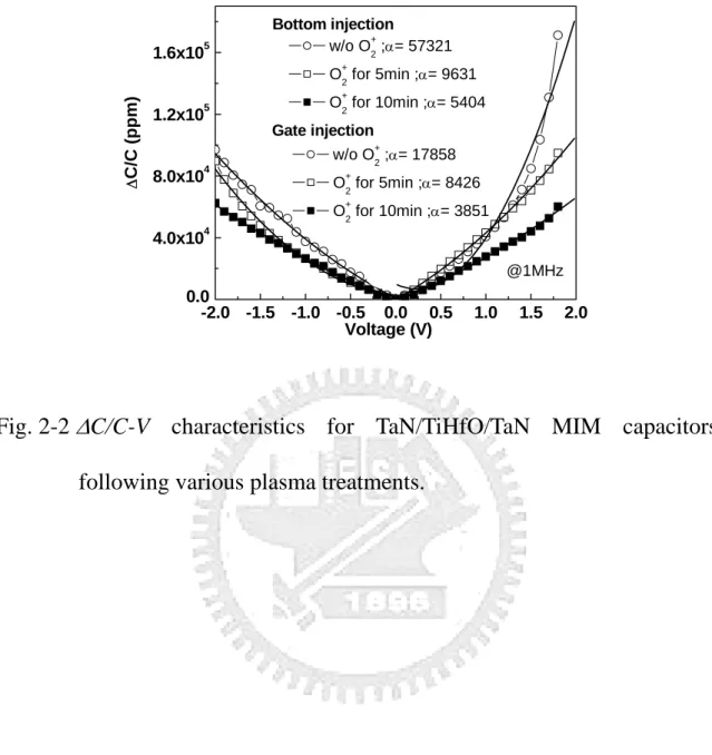
We have also measured the variation of the capacitance (ΔC/C) as a function of
voltage. In Fig. 2-2 we show such ΔC/C-V data. The voltage dependence of ΔC/C is
expressed as βV+αV2 [2-8]-[2-12], where β and α are the linear and quadratic
coefficients of ΔC/C-V, respectively. Here α is the important factor for capacitors, since
the effects of β can be compensated in the circuit design [2-8]. Increasing the exposure time of the bottom TaN to an oxygen plasma decreased α from 17858 to 3851 ppm/V2
. Since the α improves rapidly with decreasing capacitance density [2-14], further α reduction is possible at lower capacitance density used for analog/RF application.
To understand these performance improvements, we examined the devices using
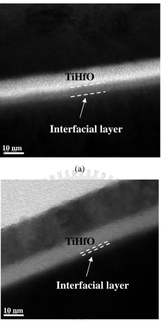
cross-sectional TEM. In Figs. 2-3 (a) and (b) we compare the TEM images for the TiHfO
structure without and with the oxygen plasma treatment. A clear interfacial region, ~3 nm
wide, can be seen in the conventional nitrogen-only plasma-treated TaN, giving a total
thickness of ~15 nm. In contrast, the combined oxygen and nitrogen plasma-treated TaN
shows reduced interfacial reactions. A thickness of ~12 nm was measured for the TiHfO dielectric – indicating a κ value of 38, at a capacitance density of 28 fF/μm2
.
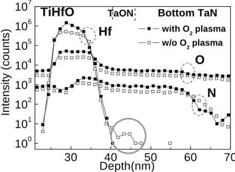
analysis in Fig. 2-5 shows that a significant improvement with less Hf diffusion is
obtained by using O2 and N2 plasma treatment.
The possible reason for the large improvement, given by the oxygen plasma
treatment, may be the larger bond enthalpy of TaO (799 kJ/mol) compared with that of
TaN (611 kJ/mol) [2-19]. When applying only a nitrogen plasma treatment, the lower TaN
will be oxidized to TaON during unavoidable PDA, due to the thermodynamically
favorable larger bond enthalpy – this would lower the capacitance density. The
significantly smaller interfacial layer with oxygen plasma treatment may be de to the
formation of high quality TaON by highly reactive oxygen plasma, which decreases
further oxygen diffusion into underneath TaN to form poor quality thermal TaON at low
temperature during PDA.
2.4 Conclusion
We have shown that a nitrogen plasma treatment cannot, alone, suppress the
interfacial layer formation that causes degraded capacitance density and leakage current
in TaN/TiHfO/TaN MIM capacitors. By using an additional oxygen plasma treatment the
interfacial reactions and growth were reduced, leading to a higher capacitance density and
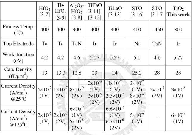
Table 2-1 Comparison of MIM capacitors having various dielectrics and metal electrodes. HfO2 [2-7] Tb- HfO2 [2-9] Al2O3- HfO2 [2-8] TiTaO [2-11]-[2-12] STO [2-16] TiHfO This work Process Temp. (oC) 400 400 400 400 400 400
Top Electrode Ta Ta TaN Ir Ni TaN
Work-function (eV) 4.2 4.2 4.6 5.27 5.1 4.6 Cap. Density (fF/μm2 ) 13 13.3 12.8 23 25.2 28 Current Density (A/cm2) @ 1V 6×10⁻⁷ 6×10⁻⁸ 5×10⁻⁹ 2×10⁻⁶ 2×10⁻⁷ 4.8×10⁻⁶ \
-1.5 -1.0 -0.5 0.0 0.5 1.0 1.5 20 25 30 O 2 Plasma 3 min O2 Plasma 5 min TaN/TiHfO/TaN 100 kHz 500 kHz Voltage (V) Cap a ci ta nce Den s ity (fF/um 2 ) W ithout O2 Plasma (a) -3 -2 -1 0 1 2 3 10-9 10-7 10-5 10-3 10-1 101 O2 plasma 3 min O2 plasma 5 min w/o O2 plasma C u
rrent density (A/cm
2 )
Voltage (V)
Gate injection Bottom injection
After O2 Plasma treatment
(b)
Fig. 2-1 (a) C-V and (b) J-V characteristics for TaN/TiHfO/TaN MIM
capacitors measured after the indicated plasma treatments.
-2.0 -1.5 -1.0 -0.5 0.0 0.5 1.0 1.5 2.0 0.0 4.0x10⁴ 8.0x10⁴ 1.2x10⁵ 1.6x10⁵ w/o O+ 2 ;α= 17858 O+2 for 5min ;α= 8426 O+ 2 for 10min ;α= 3851 Bottom injection w/o O+2 ;α= 57321 O+ 2 for 5min ;α= 9631 O+ 2 for 10min ;α= 5404 @1MHz Δ C/C ( ppm) Voltage (V) Gate injection
Fig. 2-2
Δ
C/C-V characteristics for TaN/TiHfO/TaN MIM capacitors
TiHfO
Interfacial layer
10 nm (a)TiHfO
Interfacial layer
10 nm (b)Fig. 2-3 Cross-sectional TEM images of the TiHfO structure (a) with only a
nitrogen plasma treatment and (b) with both a nitrogen and a
second oxygen plasma treatment.
(a)
(b)
Fig. 2-4 The surface roughness of bottom electrode (a) with or (b) without
O
2plasma treatment by AFM spectroscopy.
30
40
50
60
70
10
010
110
210
310
410
510
610
7TiHfO
TaON with O 2 plasma w/o O 2 plasmaBottom TaN
N
Hf
In
tensit
y (count
s)
De
O
pth(nm)
Fig. 2-5 SIMS analysis for TiHfO/TaN with or without O
2plasma treatment
Chapter 3
Low Temperature Crystallized TiO
2Dielectrics for
DRAM Application
3.1 Introduction
There is a strong desire to decrease the processing temperature of
Metal-Insulator-Metal (MIM) capacitors [3-1]-[3-16], while maintaining a high capacitance density (ε0κ/tκ) and low leakage current. This requirement is due to the low-temperature processing associated with low-κ isolation dielectrics, such as PAR. For VLSI backend integration, temperatures down to 300oC may be desirable [3-17].
Low-temperature-processed MIM capacitors would be useful in the integration of
future-generation Ge-on-Insulator (GOI) [3-18]-[3-19] and IIIV-on-Insulator (IIIVOI)
[3-20] technologies, where the device performance can be crucially dependent on the thermal processing budget. Unfortunately, most high-κ dielectrics, as used for high-density MIM capacitors, require a high process temperature to improve their quality and increase the κ value by crystallization.
Here we describe the performance of MIM capacitors processed at only 300oC. A capacitance density of 28 fF/μm2 was obtained with a leakage current of just 3×10⁻⁸
450oC-processed SrTiO3 (STO) [3-14]-[-15], and is better than that for 400oC-processed
TiLaO [3-11]-[3-12], TiTaO [3-13] and STO [3-16] capacitors. This was achieved by using a high-κ TiO2 dielectric which had a high κ value of 65, due to nano-crystal formation. This occurs at processing temperatures as low as 300oC. These MIM
capacitors have potential in analog, RF and DRAM applications and are vital for GOI
[3-18]-[3-19] and IIIVOI [3-20] technologies.
3.2 Experimental procedure
The high-κ TiO2 MIM capacitors were fabricated on standard Si wafers having a 2-μm-thick SiO2 isolation layer on the Si substrates. Then TaN, 50 nm thick, was deposited on a 200 nm Ta layer and used as the lower capacitor electrode. The TaN
surface was given an NH3 plasma treatment first [3-13]-[3-16] and then exposed to an O2 plasma – this being done to increase the oxidation resistance before the high-κ dielectric deposition and post-deposition anneal (PDA). Then 20 nm thick TiO2 dielectric was deposited at room temperature by electron-beam evaporation at a pressure of 2×10⁻⁶
torr,
followed by a 300oC PDA for 10 min in an oxygen ambient of 1 atm pressure. Finally, a
20 nm Ir layer was deposited and patterned to form the top electrode. The capacitors were 180-μm×180-μm in size, thus minimizing any complications from variations in
standard C-V and J-V measurements.
3.3 Results and discussion
In Figures 3-1 (a) and (b), we show the C-V and J-V characteristics of Ir/TiO2/TaN capacitors, respectively. A high capacitance density of 28 fF/μm2
was measured, along with a low leakage current of 3×10⁻⁸
A/cm2 at -1 V. These results are compared with other
MIM data in Table 1. Our results are an improvement over those for a Ni/STO/TaN device, which had a slightly lower density of 25 fF/μm2
and were processed at 400oC
[3-16]. Since the work-function of the Ni electrode is only slightly lower than Ir, the
better leakage in the Ir/TiO2/TaN device, when compared with Ni/STO/TaN, is due to the
larger conduction band offset (ΔEC) of the TiO2 with respect to the STO [3-21]-[3-22].
This is because the larger ΔEC and higher work function electrode will form a higher
Schottky barrier height to lower the leakage current by Schottky emission mechanism
[3-15]-[3-16]. A larger ΔEC to the metal electrode is also important for the
high-temperature leakage current at 125oC. We found a 125oC leakage current of 6×10⁻⁷
A/cm2, measured at -1 V. This is, to the best of our knowledge, better than previous data,
and isat a high capacitance density of 28 fF/μm2 [3-1]-[3-16]. Besides, a dual plasma
for TiO2/TaN with or without O2 plasma treatment on the bottom TaN. The bottom TaN
with O2 plasma treatment reduced effectively the interface reaction due to the formation
of high qualify TaON barrier layer.
A small loss tangent of 0.013 is obtained at such large 28 fF/μm2
density using
advanced four-element model and two-frequency calculation [3-23], which can be
decreased with decreasing capacitance density [3-24]. A quadratic voltage coefficient of capacitance (α) of 5010 ppm/V2
was obtained at 500 kHz, which can also be improved
rapidly with a decreased capacitance density [3-14] used for analog/RF application. A
temperature coefficient of capacitance (TCC) of 353 ppm/oC was measured even at a high 28 fF/μm2 density.
To understand the performance improvements we examined the 300oC-processed
TiO2 structure by cross-sectional TEM. As shown in Fig. 3-3, the nano-crystallization of
TiO2 is observable even at 300oC. This nano-crystallization effect yields a high κ value of
~65 for the TiO2 dielectric – and explains why the leakage current is better than that for
previous TiTaO [3-11]-[3-12] and TiLaO [3-13] MIM capacitors, shown in Table 1, which have a κ value of 45. The high κ value, in combination with the ΔEC and high
conducting electric field for both Schottky emission and Frenkel-Pool mechanism [3-15].
To study the thermal stability we annealed an Ir/TiO2/TaN capacitor at 350oC for 20
min under an N2 ambient. In Figures 3-4 (a) and (b) we display the C-V and J-V
characteristics before and after this thermal treatment. Only a small degradation of the
capacitance density and leakage current occurred, indicating the good thermal stability of
both the top Ir electrode and the TiO2 capped metal electrodes. We also note that good
thermal stability has been reported for Ir/HfAlON pMOS even at RTA temperatures of up
to 900oC [3-25].
3.4 Conclusion
We have demonstrated Ir/TiO2/TaN MIM capacitors with a capacitance density of 28 fF/μm2, along with a leakage current of 3×10⁻⁸
A/cm2 at -1 V. Since the device
processing was performed at 300oC this would permit these capacitors to be integrated into a VLSI backend, along with advanced low-κ isolation dielectrics, or with future front-end GOI and IIIVOI technologies.
Table 3-1. Comparison of MIM capacitors which have various dielectrics and metal electrodes. HfO2 [3-7] Tb- HfO2 [3-9] Al2O3 -HfO2 [3-8] TiTaO [3-11]-[3-12] TiLaO [3-13] STO [3-16] STO [3-15] TiO2 This work Process Temp. (oC) 400 400 400 400 400 400 450 300
Top Electrode Ta Ta TaN Ir Ir Ni TaN Ir
Work-function (eV) 4.2 4.2 4.6 5.27 5.27 5.1 4.6 5.27 Cap. Density (fF/μm2 ) 13 13.3 12.8 23 24 25.2 28 28 Current Density (A/cm2) @25oC 6×10⁻⁷ (1V) 1×10⁻⁷ (2V) 8×10⁻⁹ (2V) 2×10⁻⁶ (1V) 2×10⁻⁵ (2V) 1×10⁻⁷ (1V) 2.3×10⁻⁷ (2V) 2×10⁻⁷ (1V) 8×10⁻⁶ (2V) 3×10⁻⁸ (2V) 3×10⁻⁸ (1V) Current Density (A/cm2) @125oC 2×10⁻⁶ (1V) 2×10⁻⁷ (2V) 6×10⁻⁹ (1V) 5×10⁻⁸ (2V) - 6.6×10⁻⁷ (1V) 6.7×10⁻⁶ (2V) 5×10⁻⁶ (1V) - 6×10⁻⁷ (1V)
-2 -1 0 1 2 20 25 30 35 40
C~28 fF/
μ
m
2 500kHz 1MHzIr/TiO
2/TaN
Voltage (V) Ca pa cita nce De nsity (fF/u m 2 ) PDA 300 o C (a) -3 -2 -1 0 1 2 3 10-9 10-7 10-5 10-3 10-1 101 103 125oC 25 oCC~28 fF/
μ
m
2 Current densi ty (A/ c m 2 ) Voltage (V)Gate injection Bottom injection PDA 300oC
(b)
0
500
1000
1500
20
40
60
w/o O
2plasma
Ti
2p
Ta
4f
A
tom
ic
per
c
ent
(
%)
Etching time (sec)
with O
2plasma
Bottom TaN ElectrodeFig. 3-2 XPS depth profile for TiO
2/TaN with or without O
2treatment on
Nano-crystal
10 nm
Fig. 3-3 A cross-sectional TEM image of a TiO
2sample, after 300
oC
processing.
-2 -1 0 1 2 20 25 30 35 40 C~28 fF/μm2 Before 350oC N2 PDA for 20min After 350oC N2 PDA for 20min
Ir/TiO
2/TaN
Voltage (V) Capacitance Density (f F/ μm 2 )@1MHz
(a)-3
-2
-1
0
1
2
3
10
-910
-710
-510
-310
-110
110
3After 350oC N2 PDA for 20min Before 350oC N2 PDA for 20min
Ir/TiO
2/TaN
C~28 fF/μm
2Current density
(A
/cm
2)
Voltage (V)
Gate injection Bottom injection
(b)
Chapter 4
Improved High-Temperature Leakage in High Density
MIM Capacitors by Using a TiLaO Dielectric and an Ir
Electrode
4.1 Introduction
There is a continuing demand to increase the capacitance density (ε0κ/tκ) of the Metal-Insulator-Metal (MIM) capacitors [4-1]-[4-16]. To achieve this, the MIM devices have evolved by using higher κ dielectrics such as SiN [4-3]-[4-4], Al2O3 [4-6]-[4-7], Ta2O5 [4-5], HfO2 [4-8]-[4-10], Nb2O5 [4-11], TiTaO [4-12]-[4-13] and SrTiO3 (STO) [4-14]-[4-16]. Unfortunately, increasing the κ value usually decreases the conduction band offset (ΔEC) with respect to the metal electrode. For STO [4-17] ΔEC can even be
slightly negative. This low ΔEC leads to unwanted poor leakage current of MIM device at
elevated temperature [4-16], whereas such high temperature operation is unavoidable due
to the increased circuit density with higher power dissipation. Besides, although STO showed higher κ values by forming nano-crystals, this only occurs at a high process
using a high work-function Ir electrode and processed at 400oC. We measured leakage currents of 1×10⁻⁷ and 6.6×10⁻⁷
A/cm2 at respective 1 V at 25 and 125oC that are lower
than previous TiTaO and 400oC-processed STO capacitors.
4.2 Experimental procedure
The high-κ TiLaO MIM capacitors were fabricated on standard Si wafers. To permit VLSI backend integration, the process began with depositing a 2-μm-thick SiO2 isolation layer on the Si substrates. Then 50 nm TaN on a 200 nm Ta layer was deposited by
sputtering and used as the lower capacitor electrode. The TaN surface was then given a plasma treatment to increase the oxidation resistance before the high-κ deposition and post-deposition annealing (PDA) [4-5]-[4-6]. A 15 nm thick TixLa1-xO (x~0.67) film was
deposited by PVD, followed by a 400oC PDA in an oxygen ambient to reduce the defects
and the leakage current [4-3]. (The TiLaO thickness was later measured by
cross-sectional TEM.) Finally, 20 nm Ir and/or 50 nm TaN were deposited and patterned to form the top electrode. A large capacitor size of 100-μm×100-μm was chosen to avoid the size difference by lithography. The devices were characterized by C-V and J-V
measurements.
4.3 Results and discussion
summarized in Table 1. A high capacitance density of 24-24.5 fF/μm2
was measured for the TiLaO MIM devices, which gives a high-κ value of ~45 for the TiLaO dielectric. A leakage current of 2.2×10⁻⁶
A/cm2 at -1 V was measured for the TaN/TiLaO/TaN MIM
capacitor, close to that of an Ir/TiTaO/TaN device (Table 1) with a slightly lower
capacitance density. Since the work-function of the TaN on TiLaO is ~0.7 V lower than
that of Ir on TiTaO, the comparable leakage current indicates that the TiLaO is the better
choice for MIM capacitor than TiTaO. This is confirmed by the 5 times lower leakage current of 1×10⁻⁷
A/cm2 in the TaN/Ir/TiLaO/TaN device compared with the Ir/TiTaO/TaN
capacitor. This improved leakage current, at a comparable capacitance density, is due to
the higher ΔEC between metal and high-κ interface, which lowers the leakage current
exponentially. Similar lower leakage current was also reported by adding higher ΔEC
Al2O3 into HfO2 MIM capacitor [4-9]. The very small changes of J-V and C-V after
400oC N2 annealing indicates the good thermal stability, while good thermal stability of Ir
on HfAlON up to 900oC was reported for metal-gate/high-κ pMOS [4-17].
A larger ΔEC at the metal/high-κ interface is very important at 125oC, a temperature
required for both DRAM and non-volatile memory. This is shown in the comparison with o
capacitor it only increased from 1×10⁻⁷ to 6.6×10⁻⁷
A/cm2. Although the work-function of
the Ir electrode (5.27 eV) is slightly higher than Ni (5.1 eV), the improved 125oC leakage
current, can be attributed to the large ΔEC. We note that La2O3 has the highest ΔEC with
respect to Si (2.3 eV) compared with HfO2 (1.5 eV), ZrO2 (1.4 eV), Ta2O5 (0.3 eV), and
STO (-0.1 eV) [4-18].
To investigate the current conduction mechanism we plot, in Fig. 4-2, ln(J) versus
E1/2 for the TaN/Ir/TiLaO/TaN MIM capacitors:
⎟ ⎟ ⎠ ⎞ ⎜ ⎜ ⎝ ⎛ − ∝ kT V E J b 2 1 exp γ (1) 2 1 0 3 ⎟⎟ ⎠ ⎞ ⎜⎜ ⎝ ⎛ = ∞ K e ηπε γ . (2) Here K∞is the high-frequency dielectric constant (= n2). The refractive index n is 2.57 or
1.9 for TiO2 or La2O3 [4-19]), and η is 1 or 4 for Schottky emission (SE) or Frenkel-Poole
(FP) conduction, respectively. The data fitting suggests that the current conduction
mechanism of the TaN/Ir/TiLaO/TaN device changes from SE at low electric fields to FP
at higher fields. In contrast, the TaN/TiLaO/TaN devices fit an SE description at both low
and high fields.
electrodes, respectively. The large Vb difference explains the reduced leakage current and
weaker temperature dependence in the TaN/Ir/TiLaO/TaN devices. Thus low leakage current at high temperature can be obtained in MIM capacitors by combining a high-κ dielectric having a high ΔEC with a high work function metal electrode.
4.4. Conclusion
A high capacitance density and low leakage current at 125oC have been achieved in
Ir/TiLaO/TaN MIM capacitors. The device processing temperature of 400oC would
enable them to be integrated into VLSI backend technology and be used in multiple
Table 4-1. Comparison of MIM capacitors with various dielectrics and metal electrodes. HfO2 [4-8] Tb- HfO2 [4-10] Al2O3 -HfO2 [4-9] TiTaO [4-12]-[4-13] STO [4-16] STO [4-14] TiLaO Process Temp. (oC) 400 400 400 400 400 450 400
Top Electrode Ta Ta TaN Ir Ni TaN TaN Ir
Work-function (eV) 4.2 4.2 4.6 5.27 5.1 4.6 4.6 5.27 C Density (fF/μm2 ) 13 13.3 12.8 23 25.2 28 24.5 24 J (A/cm2) @25oC 6×10⁻⁷ (2V) 1×10⁻⁷ (2V) 8×10⁻⁹ (2V) 2×10⁻⁶ (1V) 2×10⁻⁵ (2V) 2×10⁻⁷ (1V) 8×10⁻⁶ (2V) 3×10⁻⁸ (2V) 2.2×10⁻⁶ (1V) 1×10⁻⁷ (1V) 2.3×10⁻⁷ (2V) J (A/cm2) @125oC 2×10⁻⁶ (1V) 2×10⁻⁷ (2V) 6×10⁻⁹ (1V) 5×10⁻⁸ (2V) - 5×10⁻⁶ (1V) - 1.3×10 -4 6.6×10⁻⁷ (1V) 6.7×10⁻⁶ (2V)
-1.5 -1.0 -0.5 0.0 0.5 1.0 1.5 20 22 24 26 28 30 32
Ir/TiLaO/TaN
C~24 fF/
μm
2TaN/TiLaO/TaN
100 kHz 500 kHz 1M Hz Voltage (V) C apacitance D ensity ( fF/um 2 ) (a) -3 -2 -1 0 1 2 3 10-9 10-7 10-5 10-3 10-1 101 103 TaN/TiLaO/TaN Ir/TiLaO/TaN Measured @ 125oC Measured @ 25oC TaN/TiLaO/TaN Ir/TiLaO/TaN Current D ensity (A/c m 2 ) Voltage (V)Gate injection Bottom injection C ~ 24 fF/μm2
-3 -2 -1 0 1 2 3 10-9 10-7 10-5 10-3 10-1 101 103 As-deposited
After 400 C N2 anneal for 20 min
Current Density
(
A/cm
2 )
Voltage (V)
Gate injection Bottom injection
-2.0 -1.5 -1.0 -0.5 0.0 0.5 1.0 1.5 2.0 10 12 14 16 18 20 22 24 26 28 30 o 2 Ir/TiLaO/TaN As-deposited (c)
Fig. 4-1 (a) C-V, (b) J-V and (c) thermal stability characteristics of
TaN/TiLaO/TaN and TaN/Ir/TiLaO/TaN MIM capacitors measured
at various frequencies, at 25 and 125
oC. The thermal stability test
was performance at 400
oC for 20 min at N
2ambient.
After N2 anneal for 20 min
Voltage (V) Capac itance D e nsity (fF/um Measured @ 500MHz
-5 10 1000 2000 3000 4000 -20 -15 -10 0 5
Ir/TiLaO/TaN
C~24 fF/μm2 Schottky emission @ 25oC @125oC Poole-Frenkel emission E1/2(V/cm)1/2 ln (J) 2000 3000 4000 -20 -15 -10 -5 0 5 TaN/TiLaO/TaN @ 25oCFig. 4-2 Measured and simulated J-E
1/2of an Ir/TiLaO/TaN capacitor. A
TaN/TiLaO/TaN device is shown, for comparison, in the insert.
@125oC Schottky emission E1/2 (V/cm)1/2 ln ( J )
1500 2000 2500 3000 3500 e-25 e-22 e-19 e-16 e-13 @125oC Gate injection TaN/TiLaO/TaN barrier height = 0.57eV
Ir/TiLaO/TaN
barrier height = 1.35eV
Schottky emission fitting J/T 2 (A/c m 2 -K 2 ) E1/2(V/cm)1/2
Fig. 4-3 The J/T
2-E
1/2plots of TaN/TiLaO/TaN and TaN/Ir/TiLaO/TaN MIM
capacitors.
Chapter 5
MIM Capacitors Using a High-
κ TiZrO Dielectric for
Analog and RF Applications
5.1 Introduction
The continuously increasing capacitance density (εκ/tκ) and preserving low leakage current are the technology trend of the Metal-Insulator-Metal (MIM) capacitors [5-1]-[5-18]. To achieve this goal, the using higher κdielectrics for MIM capacitors are required. However, the increasing κ value usually decreases the conduction band offset (ΔEC) to the metal electrode, where the ΔEC even becomes slightly negative (-0.1 eV) in
SrTiO3 (STO) [5-18]. Such small ΔEC increases the unwanted leakage current of MIM capacitors [5-16], and therefore a trade off between ΔEC and κ value is necessary. Besides, the κ value in STO is strongly dependent on the process temperature due to the formation of nano-crystals at above 450oC [5-16]. Unfortunately, such high temperature is above the maximum allowable temperature of 400oC for VLSI backend integration. In this paper, we report low leakage TiZrO MIM capacitors processed at 400oC. Using a low cost and high work-function (5.1 eV) Ni electrode, low leakage currents of 2.5×10⁻⁷ and 4×10⁻⁸
These electrical characteristics are better than previously reported TiTaO [5-12]-[5-13] and TiHfO [5-15] capacitors. Besides, a small quadratic voltage coefficient of capacitance (VCC α) of 105 ppm/V2 and temperature coefficient of the capacitance (TCC) of 156 ppm/oC were measured in the 5.5 fF/μm2 TiZrO MIM capacitor. Such excellent device characteristics are due to the higher ΔEC for ZrO2 (1.4 eV) than Ta2O5 (0.3 eV) and better κ of ZrO2 than HfO2 [5-19], [5-20]. These good devices performances of Ni/TiZrO/TaN capacitors can be used for multiple functional System-on-Chip (SoC) application.
.
5.2 Experimental procedure
The high-κ TiZrO MIM capacitors were fabricated on Si wafers. For VLSI backend integration, a 2-μm thick SiO2 isolation layer was first deposited on the Si substrates. After that, the combined bottom electrode of 200 nm Ta and then 50 nm TaN were deposited by sputtering. The TaN surface was exposed to a NH3+ plasma treatment to increase the oxidation resistance during the following post-deposition annealing (PDA) [5-5]-[5-6]. Then a 16 nm-, 47 nm- or 56 nm-thick TixZr1-xO (x~0.67) dielectric layer was deposited by physical vapor deposition. A 400oC PDA in oxygen ambient was performed to reduce the defects in TiZrO and leakage current [5-3]. Finally, a 40 nm Ni and/or 50
180-μm×180-μm was measured. The devices were characterized by C-V and J-V measurements.
5.3 Results and discussion
Figures 1(a) and 1(b) show the C-V and J-V characteristics of Ni/TiZrO/TaN and Al/TiZrO/TaN capacitors. A high capacitance density of 18 fF/μm2 was measured at 500 kHz. At -2 V, the leakage current of TiZrO MIM capacitors improves by two orders of magnitude using a high work function Ni (5.1 eV) as compared with Al (~4.1 eV) electrode. At this 18 fF/μm2 capacitance density, low leakage currents of 3.3×10⁻⁸ A/cm2 and 2.5×10⁻⁷ A/cm2 at -1 V and -2V were measured in Ni/TiZrO/TaN MIM capacitor, respectively. Table 1 summarizes the important device performance of various MIM capacitors. The Ni/TiZrO/TaN device data is better than that of the Ir/TiTaO/TaN MIM capacitors with a lower 14.3 fF/μm2 capacitance density shown in Table 1, even though higher work function Ir top electrode (~5.27 eV) is used for TiTaO capacitor than Ni electrode (~5.1eV) for TiZrO. This is mainly attributed to the larger conduction band offset of ZrO2 (1.4 eV) than that of Ta2O5 (0.3 eV) [5-19]. The device performance of Ni/TiZrO MIM capacitors is also better than the Ni/TiHfO [5-15], where higher capacitance density is obtained in Ni/TiZrO with comparable leakage current shown in
reason why ZrO2 is used in DRAM to replace HfO2 [5-20]. For analog IC application, low VCC α is required. Figure 1 (c) showed the ΔC/C-V characteristics of TiZrO MIM
capacitors, where VCC α can be extracted from the following equation: ; α and β are quadratic and linear VCC, respectively. The VCC α is better using Ni electrode than that of Al. This may arise from the higher work function of Ni than Al, which exponentially decreases the free carriers injection from electrode by Schottky emission and lower the effect of charge relaxation [5-21].
) 1 ( ) ( 2 0 + + =C V V V C α β
To further lower the VCC, we fabricated TiZrO dielectric capacitors at larger 47 and 56 nm thickness. Figures 2(a), 2(b) and 2(c) show the C-V, J-V and ΔC/C-V
characteristics of Ni/TiZrO/TaN capacitors at these TiZrO thicknesses. Low leakage current of 6.7×10⁻⁸ A/cm2 and 4×10⁻⁸ at -2 V were measured at capacitance density of 6.5 and 5.5 fF/μm2, respectively. Both the VCC α and β decrease with increasing TiZrO thickness or decreasing capacitance density. Small VCC α of 105 ppm/V2 and VCC β of -757 ppm/V at 500 kHz were obtained at a 56 nm thickness of TiZrO with capacitance density of 5.5 fF/μm2. From the experimental data presented in above Figs. 1(c) and 2(c), the VCC α improves with increasing metal work-function and dielectric thickness, where both cases give the lower charge injection into the capacitor. This is well explained by the
nearly meet the requirements of bypass capacitors used for RF circuits listed in International Technology Roadmap for Semiconductors (ITRS) at year 2012: with capacitance density >5fF/μm2, VCC ⎪α⎪ <100 ppm/V2 and VCC ⎪β⎪ <1000 ppm/V [5-1].
The temperature coefficient of capacitance (TCC) is an important factor, since modern ICs usually operate at elevated temperatures. Figure 4 shows the measured normalized capacitance as a function of temperature. Small TCC values of 179 and 156 ppm/oC were measured at 100 kHz for the 6.5 and 5.5 fF/μm2 density TiZrO MIM capacitors, respectively. The decreasing trend of TCC with decreasing capacitance density is similar to the VCC α case, which again may be related to the charge trapping and relaxation in MIM capacitors [5-21].
Such improving trend of VCC α with decreasing capacitance density of MIM capacitors is summarized in Fig. 4. Here the variation of α is plotted as a function of 1/C to show the dependence of capacitance equivalent thickness (CET=ε0κ/C). The TiZrO shows better chance to meet the ITRS requirement at 2012 than HfO2 and Ta2O5. Besides, for the same required VCC ⎪α⎪ <100 ppm/V2, the TiZrO can have higher capacitance density than using HfO and Ta O .
and 5(b) display the C-V and J-V characteristics of Ni/TiZrO/TaN device before and after thermal annealing at 350oC for 20 min under N
2 ambient. Only a small degradation of the
capacitance density and leakage current was found, which indicates the good thermal stability of both the top Ni electrode and the TiZrO dielectric.
5.4. Conclusion
We have investigated the device characteristics of Ni/TiZrO/TaN capacitors. Low leakage current and high capacitance density were obtained and better than previous reported MIM capacitors using TiTaO or TiHfO dielectric. Low leakage current, small VCC α of 105 ppm/V2 and TCC of 156 ppm/oC have been achieved in Ni/TiZrO/TaN MIM devices at 5.5 fF/μm2 capacitance density. This high performance device is capable to be integrated into VLSI backend and be used in multiple functions associated with SoC.
Table 5-1 Comparison of MIM capacitors with various dielectrics and metal electrodes. HfO2 [5-8] Tb- HfO2 [5-10] TiTaO [5-12]-[5-13] TiHfO [5-15]
ITRS @
2012
[5-1] TiZrO (This work) Top Electrode Ta Ta Ir Ni - Ni Work-function (eV) 4.2 4.2 5.27 5.1 - 5.1 C Density (fF/μm2) 13 13.3 14.3 14.35
18 6.5 5.5 J (A/cm2) @25oC 6×10⁻⁷ (2V) 1×10⁻⁷ (2V) 2×10⁻⁷ (2V) 8.4×10⁻⁸ (1V) - 3.3×10⁻⁸ (1V) 2.5×10⁻⁷ (2V) 6.7×10⁻⁸ (2V) 4×10⁻⁸ (2V) α (ppm/V2) 607 2667 634 3392α<100
3308 248 105-2.0 -1.5 -1.0 -0.5 0.0 0.5 1.0 1.5 2.0 14 16 18 20 22 24 100 kHz 500 kHz Ni/TiZrO/TaN Al/TiZrO/TaN Voltage (V) C H (fF/um 2 ) (a) -3 -2 -1 0 1 2 3 10-9 10-7 10-5 10-3 10-1 101 103 105 107 4.5eV Ni TiZrO TaN 5.1eV 4.1eV Al Ni/TiZrO/TaN Al/TiZrO/TaN Current den sity ( A/cm 2 ) Voltage (V)
Gate injection Bottom injection
0.0 -0.5 -1.0 -1.5 -2.0 0.0 6.0x10³ 1.2x10⁴ 1.8x10⁴ 2.4x10⁴ 3.0x10⁴ 3.6x10⁴ 4.2x10⁴
C~18 fF/
μm
2 α=7651 α=3308 Ni/TiZrO/TaN Al/TiZrO/TaN Δ C/C (ppm) Voltage (V) @500kHz (c)Fig. 5-1 (a) C-V, (b) J-V and (c) ΔC/C-V characteristics of Al/TiZro/TaN
and Ni/TiZrO/TaN MIM capacitors.
-2.0 -1.5 -1.0 -0.5 0.0 0.5 1.0 1.5 2.0 2 4 6 8 10 C~6.5
fF/
μm
2 C~5.5fF/
μm
2Ni/TiZrO/TaN
100 kHz 500 kHz Voltage (V) C H (fF/um 2 ) (a) -3 -2 -1 0 1 2 3 10-9 10-7 10-5 10-3Ni/TiZrO/TaN
C~6.5 fF/μm2 C~5.5 fF/μm2 Cu rren t densi ty ( A/c m 2 ) Voltage (V)G ate injection Bottom injection
![Fig. 1-1 The International Technology Roadmap of SIA for Semiconductor 2007 [1-1]](https://thumb-ap.123doks.com/thumbv2/9libinfo/8760563.208088/30.892.150.754.103.906/fig-international-technology-roadmap-sia-semiconductor.webp)
![Fig. 1-4 Static dielectric constant versus band gap for candidate gate oxides, after Robertson [1-13]](https://thumb-ap.123doks.com/thumbv2/9libinfo/8760563.208088/31.892.156.743.483.940/static-dielectric-constant-versus-candidate-oxides-after-robertson.webp)