RM04D-2
A
5.4-mW
LNA
Using 0.35-pm SiGe BiCMOS Technology for
3.1
-
10.6-GHz UWB Wireless Receivers
Ming-Da Tsai, Kun-You Lin, and
Huei Wang
Dept. of Electrical Engineering and Graduate Institute of Communication Engineering,
National Taiwan University, Taipei, 106, Taiwan, R.O.C.
Abstract - A modified low-power and low-noise
distributed amplifier for ultra-wideband (UWB) radio
systems is first proposed to overcome the bottleneck of conventional DA. The UWB LNA achieves 10-dB gain with 5.4-mW power consumption, and 3-dB roll-off up to 10.6 GHz, The measured noise figures are lower than 5.5 dB from 3.1 to 10.6 GHz with 1.5 V supply. The output PldB is -5.8 dBm and input IP3 is -4 dBm from 1.5-V supply. The
MMIC occupies total chip size of only 0.47 mm2 including a l l testing pads.
Index Terms - RFIC, low power, Silicon, SiGe BiCMOS, UWB, LNA.
I
, TNTRODUCTIONUltra-wideband (UWB) communication systems have received significant attention from industry, media and
academia recently. UWB system is a new wireless technology capable of transmitting data over a wide spectrum of frequency bands with very low power and high data rates 111-131. Among the possible applications,
UWB technology may be used for imaging systems, vehicular and ground penetrating radars, and communications systems. Up to now, two possible
approaches have emerged to exploit the allocated spectrum. One is a multiband approach, with fourteen
500-MHz subbands, OFDM modulation, and the other is
the impulse radio. Although the UWB standard (IEEE
802.15.3a [2]) has not been completely defined, most of the proposed applications are allowed to transmit in a
band between 3.1-10.6 GHz.
In recent years, narrow-band LNA designs have employed inductive source degeneration to achieve good input matching [4]-171. This technique also yields nearly optimal noise figure at the resonance frequency of the input network. Some low-noise amplifiers have been demonstrated for wideband applications
[XI-[
161. A30-mW high-gain LNA using LC-ladder matching network was proposed and implemented in 0.18-ym SiGe HBT technology [SI. A 3.4-6.9-GHz LNA with inductive source degeneration consumes 3.5 mW for applications of low-end UWB radio spectrum [9]. A DC-7.S GHz LNA
using 0.25-pm SiGe BiCMOS process was. demonstrated
for UWB and optical communication [lo]. A Chebyshev matching CMOS
LNA
provides good input return losswith the noise figure from 4 to 9 dB in the desired band
[12]. A conventional CMOS distributed amplifier (DA)
can cover full-band
UWB
with lowNF,
but consumes high dc power [ 111.Distributed amplifier (DA) is a well-known wideband amplifier potentially from DC to ultra-high frequency. In design of wideband distributed amplifiers, artificial transmission lines can be realized by multi-order LC
ladder network. Distributed amplifier features good gain flatness, return losses, flat group delay and noise figure
(NF) over a wide frequency band, making possible its applications for a low-noise millimeter-wave receiver for
digital optical communication and other pulse applications. However, for low-power UWB system requirement, the power consumption issue makes the conventional distributed amplifier difficult to be integrated into low-power single radio chip.
In this paper, we proposed a new modified low-power low-noise DA for UWB applications to overcome the bottleneck of conventional DA. Tnstead of off-chip bias-T and on-chip collector line termination resistor, the bias is
through output matching network to achieve low power operation. With the bias network, the supply voltage can operate as low as 1 V even though the active gain cells
are
cascode configuration.This
MMIC
fabricated
in 0.35-pm SiGe BiCMOS can achieve a good flatness ofnoise figure and gain frequency responses with only 5.4
mW for possible integrated in single UWB radio chip.
11. MMIC PROCESS
The UWB LNA was implemented using TSMC
commercial 0.35-pm 3P3M SiGe BiCMOS technology, which provides three poly layers for the emitters and
bases of the SiGe hetero-junction bipolar transistor (HBT) and the gates of the complementary MOS (CMOS)
transistors; three metal layers for interconnection. The
HET manufactured in this technology offer maximum
335
oscillation frequency
vmx)
of 57 GHz.
The
SiGe
BiCMOS process with low-resistivity substrate (- 10 S h )
provides monolithic inductors with quality factor below
10. A MIM capacitor of lfF/pm* has been developed
using oxide inter-metal dielectric. Polysilicon resistors, with several Ql* and kRI-, are provided by choosing the individual dose of' ion-implantation separately from the gate electron doping process.
111. CIRCU~T
DESIGN
Low power operation is one of main design goals for
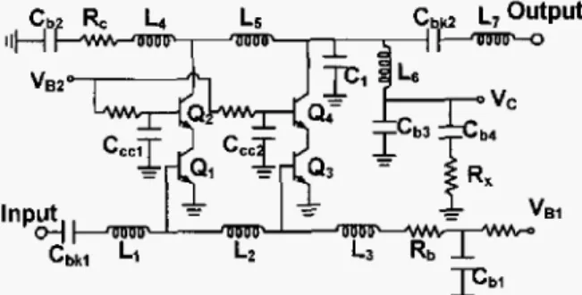
UWB systems. Conventional DAs, as shown in Fig. 1,
have to be biased through on-chip collector-line termination (Rc,) or off-chip bias-T. For on-chip bias, the bias voltage VK is difficult to achieve low-voltage operation since the voltage headroom in collector-line termination results in higher power consumption. For off-chip bias V,, the bias-T can provide lower supply voltage than on-chip bias, but it is impossible to be integrated with other front-end circuits into single RF
chip.
To overcome this integration difficulty and high power consumption issues, we proposed a new design concept
for
U W B
applications. Figure 2 shows the circuit schematic of the modified distributed type low-noise amplifier. Since the UWB system only need band-pass feature, the lower-band response of conventional distributed amplifier is not needed. This indicates the conventional base and collector resistor(R,
and RJ need not be 50 ohm to satisfy impedance match at low frequency (e.g. below 3.1 GHz). Instead, the output impedance matching can be achieved by adding C, and L,.For R, is much larger than 50 0 , the low-frequency
matching is improved by L,, while C , can improve high-frequency return loss. In Fig. 2, the supply voltage
Vc is biased through shunt inductor L, of the output
matching network instead of collector resistor R,. The supply current can flow through L, to active devices without undesired voltage drop in R,. The C,,, is used to
prevent current to ground. The C,, C, and Rx serve as bypass network for supply voltage V,.
The chip photograph is shown in Fig. 3 with chip size
of only
0.47 mm2
including allRF
and DC testing pads.IV.
MEASUREMENT
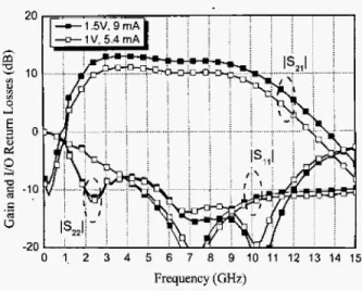
RESULTSThe UWB LNA was measured using on-wafer probing with GGB ground-signal-ground (GSG) probes. Figure 4 shows the measured power gain and inputloutput return losses at
I
V/5.4mA and 1.5VDmA conditions. The powergain is 10 dB and 12 dB for consuming 5.4 mA and 9 mA,
respectively, with 3-dB roll-off up to 10.6 GHz. The input
and output return losses are both better than 7 dB in the entire desired band. The measured noise figures from 1-V and 1.5-V supply are shown in Fig. 5. The flat noise figure is about 4.5 dB from 3 to 8 GHz, and lower than 4.4 and 5.5 dB at 10.6 GHz at 1-V and 1.5-V supply, respectively. The measured feu, vs. Pin at 10 GHz are shown in Fig. 6 , which indicates an input P,, of -13.6
dBm. The measured third-order inter-modulation distortion (IMD3), as shown in Fig. 7, is -52 dBc at 10
GHz
with input power of-30 dBm,
which indicates theIIP3
of
-4
dBm.Bias-T
vo,
-
T
-
Fig. I , Conventional distributed amplifier.
I &
-
Trm
Inp3 C b 3 L2
m
p
Fig. 2. Modified low-power and low-noise distributed amplifier
for UWB LNA applications.
Fig 3. Chip photograph of UWB LNA (size: 0.72 mm X 0. 5 mm).
-20
0 1, 2 3 4 5 6 7 8 9 1 0 1 1 1 2 1 3 1 4 1 5
Frequency (GHz)
Fig. 4. The measured power gain and input/output return losses at 1V/5.4mA and 1.5V/9mA.
1
1 2 3 4 5 6 7 8 9 1 0 1 1 1 2
Frequency (GHz) Fig. 5 . Measured noise figure for the UWB LNA.
-1 0 -20 -30
z
4 0 m 3 E -50 -60 -70 -80 a v1 -901
9 98 9 99 1000 1001 1002 1003 Frequency (GHz)Fig. 7. Measured two-tone test at 10 GHz with input power of
-30 dBm.
V. CONCLUSION
A low-power and low-noise amplifier for
3.1- 10.6-GHz ultra-wideband radio systems is first proposed in this paper. The broadband amplifier is based
on distributed amplifier with on-chip low supply voltage
operation to achieve low-power performance. The MMIC achieves IO-dB gain with 5.4-mW power consumption, and a 3-dB roll-off up to 10.6 GHz. The
I/O return losses are better than 7 dB. The measured
noise figures are less than 5.5 dB from 3.1 to 10.6 GHz
with 1.5 V supply. The output P,,, is -5.8 dBm and input
IP3 is -4 dBm from 1.5-V supply. The chip size is only
0.47 mmz including all testing pads. Table I summaries the recently reported LNAs for UWB applications. This
MMIC is indeed the first 3.1-10.6-GHz UWB LNA with a good flatness of noise figure and gain frequency
responses, miniature die size and lowest power consumption.
ACKNOWLEDGEMENT
This work is supported in part by the MediaTek Fellowship and National Science Council of Taiwan,
R.O.C. (NSC 93-2219-E-002-01 6, NSC
93-22 19-E-002-024, NSC 93-221 3-E-002-033, and NSC
93-2752-E-002-002-PAE). The chip is fabricated by
Taiwan Semiconductor Manufacturing Company (TSMC)
through Chip Implementation Center (CIC) of Taiwan,
R.O.C.
I"
-70 -60 -50 4 0 -30 -20 -10
Input Power (dBm) Fig. 6 . Measured P,, vs. Pin at 10 GHz.
REFERENCES
D.
Porcino and W. Hirt, “Ultra-wideband radio technology: Potential and challenges ahead,” IEEE Commun. Mug., vol.4, pp. 6674, July 2003.
FCC, “Final Rule of the Federal Communications Commission, 47 CFR Part 15, Sec. 503,” Federal Regisfer,
vol. 67, no. 95, May2002.
httD://www. ieeeXO2.nrdl S/~ub/TG3a.html.
D. K. Shaffer, and T. Lee, “A 1.5-V, IS-GHz CMOS low
noise amplifier, ‘‘ IEEE J. Solid-State Circuits, vol. 32, pp. 745-759, Jun 1997
M. D. Tsai, K. Wang, J. F. Kuan, and C. P. Chao, “A
miniature 4.3-7-GHz, 1-V CMOS LNA with helical inductors,” in IEEE European Microwave Conference,
Amsterdam, Oct. 2004.
T. K. K. Tsang and M. N. El-Gama], “A fully integrated 1
V 5.8 GHz bipolar LNA,” in Pruc. ZEEE Int. .Symp. Circuits and System (ISCAS’OI), vol. 4, pp. 842-845, May 2001.
E. Imbs, 1. Telliez, S. Detout, and Y. Imbs, “A
low-cost-packaged 4 . 9 4 GHz LNA for WLAN application,” in IEEE MTT-SDig., vol. 3, pp. 1569-1572, June 2003.
A. Ismail and A. Abidi, “A 3 to lOGHz LNA using a
wideband LC-ladder matching network,” International Solid-State Circuit Cunf: Dig. Tech. Papers, pp. 384-385,
Feb. 2004.
D. Barras, F. Ellinger, H. Jackel, and W. Hirt, “A low
supply voltage SiGe LNA for ultra-wideband frontends,”
IEEE Microwave and Wireless Component Letters, vol. 14, no. I O , Oct. 2004
[lo] F. Ellinger, D. Barras, M. Schmatz, and H. Jackel, “A
low-power DC-7.8 GHz BiCMOS LNA for UWB and Optical communication,” in IEEE MTT-S Dig., pp. 13-16,
June 2004.
[ l l ] R. C. Liu, C . S. Lin, K. L. Deng, and H. Wang, “A
0.5-14-GHz 10.6-dB CMOS Cascode Distributed Amplifier,” IEEE VLSI Circuit Symp., pp.139-140,2003
[I21 A. Bevilacqua and Ali M Niknejad, “An ultra-wideband
CMOS LNA for 3.1 to lO.6GHz wireless receivers,”
Internariunal Solid-state Circuit Con$ Dig, Tech. Papers,
pp. 382-383, Feb. 2004.
[I31 W. Lee and I. W. Filanovsky, “2 V 3 GHz low-noise bipolar wideband amplifier,” in Proc. Canadian CO$ Electrical Compurer Engineering, pp. 627432,,May 1999.
[I41 J. Sadowy et al., “Low noise, high linearity, wide bandwidth amplifier using a 0.35pm SiGe BiCMOS for
WLAN applications,” in IEEE Radio Frequency Integrated Circuits (RFIC) Symp., pp. 217-220, June 2002.
[15] H. Ainspan, M. Sower, J . - 0 . Plouchart, and J. Burghartz, “A 6.25-GHz low DC power low-noise amplifier in SiGe,” in ZEEE Custom Integrated Circuits Conf , pp. 177-180,
May 1997.
[16] F. Bruccoleri et al., “Noise canceling in wideband CMOS LNAs,” International Solid-state Circuir Con$ Dig. Tech.
Papers, pp. 406-407, Feb. 2002.
Table I
RECENTLY REPORTED PERFORMANCES OF UWB LOW NOISE AMPLIFIERS.