國
立
交
通
大
學
電機學院 IC 設計產業研發碩士班
碩
士
論
文
一個 1.25GHz具有高解析度與 8 個相位輸出
之數位控制震盪器,應用於全數位鎖相迴路
A 1.25GHz digitally controlled oscillator with
high-resolution and 8-phase output for ADPLL
研 究 生:楊永祥
指導教授:蘇朝琴 教授
之數位控制震盪器,應用於全數位鎖相迴路
A 1.25GHz digitally controlled oscillator with
high-resolution and 8-phase output for ADPLL
研 究 生:楊永祥
Student:Yung-Hsiang Yang
指導教授:蘇朝琴 教授
Advisor:ChauChin Su
國 立 交 通 大 學
電機學院 IC 設計產業研發碩士班
碩 士 論 文
A ThesisSubmitted to College of Electrical and Computer Engineering National Chiao Tung University
in partial Fulfillment of the Requirements for the Degree of
Master in
Industrial Technology R & D Master Program on IC Design
October 2007
Hsinchu, Taiwan, Republic of China
中華民國九十六年十月
之數位控制震盪器,應用於全數位鎖相迴路
研究生:楊永祥 指導教授:蘇朝琴 教授
國立交通大學電機學院產業研發碩士班
摘要
現代的系統單晶片(SoC)需要晶片內在的時脈產生器以及產生許多不同的頻 率,來提供給其他子系統使用,一般常用鎖相迴路為基礎的時脈產生器來達成此 任務;然而,鎖相迴路參數為了減少抖動量以及保持迴路的穩定度,因而必須依 照輸出頻率以及頻率產生倍數來調整,現有之類比電路方式需要較長的設計週 期。 本論文中,為了大幅降低高速傳輸之接收器硬體銷耗及設計的難度,提出了 一個可操作在高振盪頻率(Giga Hz)、高解析度、多重相位(8 個相位)輸出之數位 控制振盪器電路(DCO),此 DCO 將應用於”8-phase output 之 1.25GHz 的 ADPLL”, 而此 ADPLL 再將應用於具有”2.5Gb/s 之 data-transceiver”。為了減少鎖相迴路之 抖動量,所以,提出在數位控制振盪器中利用傳輸閘的寄生電容差值, 作為數位 控制之延遲單元,藉此提高數位控制振盪器電路之時間解析度。在微調上時間解 析度能夠依照使用驅動細胞單元的能力及數位控制之延遲單元的電容差異,作不 同的選擇,相對於使用 OAI-AOI 細胞單元或三態緩衝器矩陣,具有較線性的時 間解析度。 所提出的電路架構將被實現在 TSMC 0.18μ m 1P6M CMOS 製程,晶片面積 為310μm×220μm (不包含 PAD),其操作頻率範圍為 1.06GHz 到 1.50GHz,平 均的時間解析度為 0.38ps,當振盪頻率為 1.25GHz,其功率消耗為 34.1mW。 索引詞彙—高時間解析度,數位控制振盪器,全數位鎖相迴路high-resolution and 8-phase output for ADPLL
Student:
Yung-Hsiang Yang
Advisor: ChauChin Su
Industrial Technology R & D Master Program of
Electrical and Computer Engineering College
National Chiao Tung University
Abstract
Modern system-on-a-chip(SoC) processors often require on-chip clock generation and multiplication to produce several unrelated frequencies for other sub-systems. The PLL-based clock generator is a common way of frequency multiplication to accomplish the task. However, the loop parameters must be adjusted to minimize jitter performance and insure stability for each output frequency and multiplication factors. Conventional analog skills suffer from long design cycle.
In order to reduce the hardware overhead and the design complexity of high speed transceiver, the proposed digitally controlled oscillator has high operation frequency (GHz), high timing resolution, and multi-phase output (8-phase). The proposed DCO can be applied to “a 1.25GHz ADPLL with 8-phase output” and “a 2.5Gb/s data-transceiver architecture”. In order to reduce jitter of PLL, therefore, we propose the digitally controlled oscillator (DCO) with novel digital controlled delay cell based on parasitic capacitance difference of transmission gates. This method can enhance the timing resolution of the digitally controlled oscillator (DCO). The timing resolution in fine-tuned stage can be decided from different driving cells and capacitance difference of each digital controlled delay cell. Thus, a high resolution DCO with better timing linearity as compared with OAI-AOI cell or tri-state inverter matrix is achieved.
The proposed digitally controlled oscillator circuit is designed using TSMC 0.18μ m 1P6M CMOS process with active die area of 310μm×220μm. The operation frequency range is 1.06GHz to 1.50GHz. Average timing resolution is 0.38ps. The total power consumption of the proposed DCO is 34.1mW when oscillate frequency is 1.25GHz.
在這個時候最適合靜下心來,回想這些日子來,所歷經的人、事、物;在就 學及離開工作崗位之前,由於有公司主管的鼓勵及體諒,讓我能很順利來這求得 新知,並且在我離開公司之際,還默默的幫我跟公司爭取到一些福利,那正像是 寒冬裡暖暖的陽光。 在求學當中,很感謝父母親的支持與體諒,在這段時間中無法替家裡分擔經 濟及不常參與家裡的活動;還需感謝同學及同事們,若是遇到經濟困難之時,他 們皆會很有義氣挺到底,讓我深深的體會到雪中送炭與錦上添花的差別。 在實驗室部份,當然需感謝學長們的照顧,謝謝鴻文、仁乾,在我有疑問之 時都會熱心指導我,給予我許多晶片製作經驗上的指導;謝謝丸子,很用心的建 置實驗室裡的工作站及電腦設備,讓我在設計晶片時能無後顧之憂;還要謝謝昱 輝、盈杰,瑛佑、阿達、阿銘、智琦、楙軒、宗諭、小冠、匡良、順閔等諸位學 長的細心指導;感謝我的同學及學弟們:忠傑、教主、Snoopy、方董、小馬、議 賢、威翔、村鑫、存遠、雅婷、子俞、碩廷、孔哥、阿伯、挺毅、季慧,每位都 在生活和課業上給了我許多的照顧及幫助,大家的友誼豐富了我在實驗室的生 活,留下令人難忘的美好回憶。當然,還有助理雅雯、俊秀、上容,感謝妳們對 於我們的照顧及幫忙。 最後要謝謝用心指導我的 蘇朝琴老師,感謝您這兩年來花了許多時間讓我 了解做研究的方法和態度,此外,老師教導我的,除了專業領域的知識及技術, 還有待人處事應有的態度,讓我了解到「遇到困難時,必須以勇敢、積極的態度 去面對它並克服它,千萬不能有逃避的想法,且不可以有後悔的想法,要堅持此 信念,做事才會成功。」我相信對我未來在工作上也會有很大的幫助。在這邊說 一聲老師謝謝您! 楊永祥 2007/10/05
Chapter 1 Introduction ...1
1.1 Motivation...1
1.2 Thesis Organization ...3
Chapter
2 Overview of Clock Generators with Phase Locked Loop……4
2.1 Introduction...4
2.2 PLL Basics……….5
2.3 Summary……….14
Chapter 3 Clock Generation Circuits Classification...15
3.1 Introduction...15
3.2 The Analog Clock Generators...15
3.3 The Digital Clock Generators ...16
3.4 Analysis of the DCO Category ...17
3.5 Summary ...23
Chapter 4 Digitally Controlled Oscillator with High Resolution and
8-Phase Output...24
4.1 Introduction...24
4.2 Basic Concepts of Digitally Controlled Oscillators...25
4.3 The Proposed Fine Tune Delay Cell with High Resolution...31
4.4 Structure of the Proposed DCO ...36
4.5 Simulation Results and Layout ...41
4.6 Comparisons and Summary ...46
Chapter 5 Conclusions ...….47
5.1 Conclusions...47
Figure 1.1 Data transceiver and PLL circuit block ...3
Figure 2.1 Block diagram of an analog PLL...5
Figure 2.2 Simple implementation of a first order loop filter...6
Figure 2.3 Magnitude response Second order loop transfer function...7
Figure 2.4 Three state phase frequency detector and PFD state diagram...7
Figure 2.5 Block diagram of a digital PLL with digital block ...9
Figure 2.6 Block diagram of an all digital PLL ...9
Figure 2.7 ADPLL with fixed high speed clock to form the DCO ...10
Figure 2.8 ADPLL with direct DCO synthesis clock ... 11
Figure 2.9 Function block of ADPLL ...12
Figure 3.1 A simple ring oscillator ...16
Figure 3.2 All digital ring oscillator ...16
Figure 3.3 Ring oscillator frequency vs. ring delay...17
Figure 3.4 A typical ring-oscillator...17
Figure 3.5 Modified architecture ...17
Figure 3.6 An improved DCO architecture...19
Figure 3.7 Structure of the cell-based DCO...19
Figure 3.8 DCO using parallel tri-state inverters to adjust frequency ...20
Figure 3.9 8-cell DCO with control bit...21
Figure 3.10 Structure of DCO in [16] ...21
Figure 3.11 An improved DCO architecture...22
Figure 4.1 The DCO constructed with the DAC and the VCO ...26
Figure 4.2 The DCO constructed with the DAC and the VCO in [23]...26
Figure 4.3 The DCO constructed with high speed clock and divider...27
Figure 4.4 The DCO constructed with variable length ring oscillator...27
Figure 4.5 General mechanism for enhance of fine tune in the DCO...28
Figure 4.6 The mechanism are to adjust the resistance ...28
Figure 4.7 The mechanism are to adjust the capacitance...29
Figure 4.8 a multiplexer and two identical buffers structure ...30
Figure 4.9 replace the multiplexers and the buffers by NAND gates ...30
Figure 4.12 Conventional control mechanism with shunt capacitor...32
Figure 4.13 Proposed delay cell with transmission gate...33
Figure 4.14 The gate capacitance of transmission gate ...34
Figure 4.15 High resolution delay cell...35
Figure 4.16 High resolution delay cell simulation result...35
Figure 4.17 The proposed DCO architecture...37
Figure 4.18 The proposed DCO-cell architecture...37
Figure 4.19 The trigger circuit of the DCO ...37
Figure 4.20 The small-signal model of the DCO-cell...38
Figure 4.21 The parameter of the DCO-cell ...38
Figure 4.22 Influence of PVT variations on the controllable frequency range...41
Figure 4.23 The clock period range of the DCO at three different corner cases ...42
Figure 4.24 Tuning range of medium stage ...42
Figure 4.25 Tuning range of fine stage ...43
Figure 4.26 The coarse-code vs. medium-code period overlap diagram...43
Table 2-1 Phase Lock Loop comparison...14
Table 3-1 Characteristics of various clock generation circuits ...23
Table 4-1 The form of period overlap...44
Table 4-2 The summary of the performance...45
Chapter 1
Introduction
1.1
Motivation
Traditionally, phase locked loop based clock generators for microprocessor are the common way of frequency multiplication from a low frequency reference clock, typically from quartz oscillator. As VLSI technology grows up rapidly, the advance of semiconductor process enable the successful realization of system-on-a-chip (SoC). Modern SoC processors integrate both analog and digital real-time functions. An off-chip clock costs power to generate and to distribute on the PC-board. In addition, the ability to oscillate at different frequencies reduces costs by eliminating the need for additional oscillators to a system. Such applications often require on-chip clock generation and multiplication to produce several unrelated frequencies for digital signal processing, I/O interfaces, as well as sampled analog sub-systems [1].
One solution is to create one PLL-based clock generator running at a high frequency that can then be divided down to obtain all the desired frequencies [2]. The disadvantage of this approach is the high power consumption and stringent jitter requirements. Another approach is to have a dedicated PLL for each clock domain.
This solution is very costly in term of power and area.
In addition, most PLL design use mixed signal and full custom design techniques, which can not be fully integrated in digital environment. Due to time-to-market issue, the design cycle remains the same or even shorter. Thus in System-on-a-Chip (SoC) designs [3], each module had better to be reusable and process portable, so that the total design time can be reduced. As a result, how to design a synthesizer clock generator in an efficient way becomes more important.
The all digital PLL have several advantages over their analog counterparts. Firstly, traditional analog loop filter costs a lot of chip area. Using digital loop filters gives benefits such as robustness against noise, and also the ability to design higher order filters without much extra power consumption and areas penalty. Secondly, analog component are vulnerable to DC offset and drift phenomena that are not present in equivalent digital implementations [4].
In order to avoid the disadvantages of analog circuits, an All Digital
Phase-Locked Loop (ADPLL) has been developed because it has better
programmability, stability, and portability over different processes. It can reduce the system turn around time. The ADPLL has some unique advantages such as high noise immunity, short turnaround time, low power consumption, etc. And, this cell-based approach is also suitable for automatic synthesis of ADPLL.
However, due to the limitations of cell-based design, it is difficult to achieve a low-jitter, low-power, and high resolution all-digital cell-based clock generator. So, how to overcome the limitations of standard cells to build a high resolution delay cell with better linearity and less power consumption for DCO are the challenges for our research.
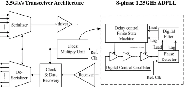
In order to reduce the hardware overhead and the design complexity of high speed transceiver (Figure 1.1), the proposed digitally controlled oscillator has high operation frequency (GHz), high timing resolution, and multi-phase output (8-phase). The proposed DCO can be applied to “a 1.25GHz ADPLL with 8-phase output” and “a 2.5Gb/s data-transceiver architecture”, as shown in Figure 1.1. The DCO is consisted of four delay elements with differential operation frequency and 8-phase output. In this thesis, a systematic design method for the DCO design is also presented. As a result, the design methodology proposed can reduce design time and design complexity of the DCO, making it very suitable for SOC applications.
Figure 1.1 Data transceiver and PLL circuit block
In Chapter 1, we introduce that diffe
lain an overview of PLL related techniques for clock gene
This chap
This
, the conclusions of this work are summarized. All the simulation resul
1.2
Thesis Organization
This thesis is organized into five chapters.
rent clock domains are required in a SoC chip. This motivation and design targets of the DCO are explained.
In Chapter 2, we exp
rator. Properties of analog, digital PLL as well as charge-pump PLL are addressed. Then, all-digital PLL with different DCO approaches are discussed. The design trade-off of clock generator with different PLL architecture is also investigated.
In Chapter 3, we explain an overview of some existing DCO structure. ter explains the most important features of conventional clock generators. As highlighted in the abstract, the focus of this thesis is on the digital clock generation method. Analog clock generators are thus only mentioned, and not explained in detail.
In Chapter 4, we first introduce the fundamental of digitally controlled oscillator. chapter also introduces different approaches to enhance the fine tune solution of the DCO. Then, the chapter explains the operation of digitally controlled delay cells with transmission gates design. And, we apply the digitally controlled delay cell to build high resolution digitally controlled oscillator. Then, we propose a novel digitally controlled oscillator structure. A detailed description of the circuits and experimental results are given.
In Chapter 5
ts are also summarized in this chapter.
Chapter 2
Overview of Clock Generators with
Phase Locked Loop
2.1
Introduction
Several methods exist for realizing frequency multiplication: phase locked loops (PLL)[5,6] , delay locked loops (DLL)[7], and direct digital synthesis (DDS) in [8]. The basic concept of the DLL is similar to PLL. The major difference is the voltage controlled delay line (VCDL) in the DLL and the voltage controlled oscillator (VCO) in the PLL [9]. Each of these methods has advantages and disadvantages for frequency multiplication. DLL approaches may offer better jitter performance than PLL approaches, because the noise induced by the power supply or substrate noise disappears at the end of the delay line. However, DLL based methods are not suitable for wide multiplication range applications. The direct digital synthesis (DDS) in [8] applied accumulator and D/A converter mechanism for the frequency synthesis. Therefore, we only focus on the PLL approach in this work.
The organization of this chapter is as follows. Section 2.2 describes the preliminary knowledge of analog and digital PLLs, basics of all digital PLL and digitally controlled oscillators applications. Design trade off in different PLL
architecture is discussed in section 2.3 .
cs
on principle is summarized in this section and the steps towards digital PLL are described
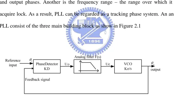
The PLL characteristics are determined by the characteristics of phase detector, ltage controlled oscillator and low pass filter. [5,6] indicated two factors that influence the performance. One is the phase error – the difference between the input
d output phases. Another is the frequency range – the range over which it will acquire lock. As a result, PLL can be regarded as a tracking phase system. An analog
L consist of the three main building block as show in Figure 2.1
2.2
PLL Basi
PLL based clock generator has been widely used in the industry. The operati
in the subsequent sections.
Analog PLL
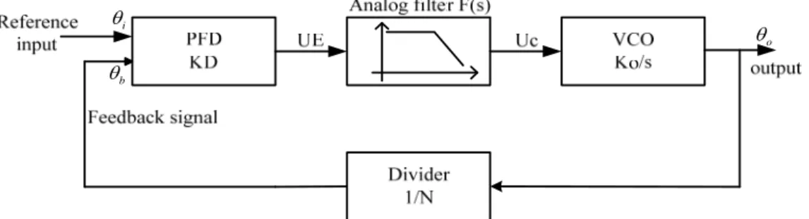
vo an PL i θ o θFigure 2.1 Block diagram of an analog PLL.
• Phase detector: It compares the phase of the input signal (reference signal) with the phase of the feedback signal. The output of the PD is ideally proportional to the phase differenceθe.
( ) ( ( ) ( )) ( )
d d i o d e
U s =K θ s −θ s =K θ s
whereK is the PD gain in [V/rad], d θiandθoare the phase of the input and output signals respectively.
with the transfer functionF s( ).
( ) ( ) ( )
c d
U s =U s ⋅F s
r: The VCO translates the filter output into a frequency. Due to the transformation of the phase information into a frequency, • Voltage controlled oscillato
it has the characteristic of an integrator with gainK [rad/sV]. o
( ) c o U s K o S θ = ⋅
The transfer function of the closed loop becomes the
( ) ( ) ( ) ( ) ( ) i s S KF s o s KF s H s θ θ + d o = = with K =K K
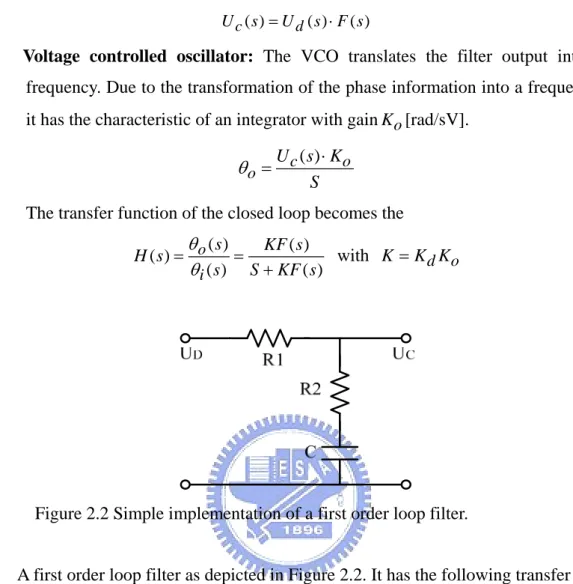
Figure 2.2 Simple implementation of a first order loop filter.
A first order loop filter as depicted in Figure 2.2. It has the following transfer function: 2 1 2 1 ( ) 1 ( SR C F s S R C R C) + = + +
So, the overall loop transfer function is a second order loop with a low pass characteristic. The natural frequency is
1 2 D o n K K R C R C ω = + and the damping factor becomes
2 1 ( ) 2 n D o R C K K ω ζ = +
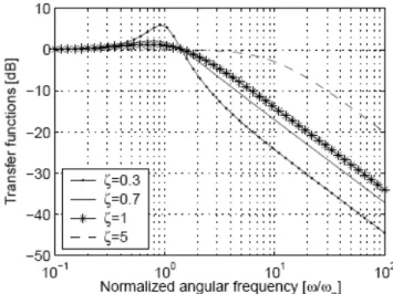
A PLL uses a first order loop filter is therefore a second order system. Figure 2.3 shows the transfer functions of a second order loop for various damping factorsζ .
Figure 2.3 Magnitude response Second order loop transfer function.
Digital PLL
The digital phase locked loops differ form their analog counterparts in that input, output, and feedback signals are digital. The phase frequency detector (PFD) is a popular replacement for analog phase detectors. It consists of a state machine with three states (‘low’, ‘zero’, ‘high’). As illustrated in Figure 2.4, the transitions between
the states are triggered b ’) and feedback
signal (‘Fb’). If it the PLL is Locked, the states ‘low’ and ‘high’ are activated only
te machine remain in ‘low’ or ‘high’ state represents the phase error [10]. y the rising edges of the reference input (‘Ref
during extremely short time spans. During the phase locking process the relative time that the sta
Figure 2.4 Three state phase frequency detector and PFD state diagram .
phase locking, the frequency of the VCO must be locked. During this phase, the PFD produces an output signal corresponding to the frequency error. Incorrect locking on an integer multiple of the desired VCO frequency is therefore not possible. The outputs of the PFD are usually combined to control a tri-state butter that remains in high-impedance during state ‘zero’ and outputs logic ‘1’ and ‘0’ in the states ‘high’ and ‘low’ respectively. This signal is then directly passed to an analog loop filter that controls the VCO. The phase detector’s gain depend on the output voltage levels of the tri-state buffers [10]:
d K 4 high low d U U K
π
− =With the binary clock in digital signals, usage of frequency dividers is simple. In l PLL contain a frequency divider in the feedback path. It allows to gene
fact, most digita
rate VCO output frequencies that are an integer multiple of the reference input frequency. The division ratio N has an impact on the overall PLL gain.
( ) ( ) o fb s s N θ θ = d o K K K N =
When the PLL has locked, the output of the PFD is permanently on high impedance, thus no current is flowing to the loop filter. The charge on the loop filter capacitance is kept constant (beside leakage effects) unit the PFD output is activated. he loop filter depicted in Figure 2.2 works thus as an integrator. The loop filter’s transfer function can then be approximated with
T 2 1 2 1 ( ) ( ) SR C F s S R C R C + = + with natural frequency
1 2 n K R C R C ω = + , d o K K K N = and damping factor
2
2
nR C
ω ζ =
The digital blocks of the digital PLL (Figure 2.5, the PFD and the divider are digit
control blocks. The analog parts (LPF and VCO) are often located off chip. Then, the al block) can be integrated in a SoC, It can close to the network interface and
one bit representation of the phase error by the PFD is very advantageous. Since it only one pin is used to transfer the digital phase information to the analog loop filter. In total two pins are required one tri-state output and one input for the VCO output signal. b θ i θ o θ
Figure 2.5 Block diagram of a digital PLL with digital block.
of continuous voltages. Thus, the phase frequency detector introduced in section 2.2.2 is modified to output a quantized number representing the phase error.
As shown in Figure 2.6, the ADPLL is composed of a digital phase frequency
to control the DCO. The output of the DCO is sent to the divider to divided into the lower frequency range. The divider sends the divided clock to the PFD and completes
All Digital PLL
In all-digital PLLs (ADPLL) all analog building blocks are replaced by a digital representation. All relevant PLL signals are binary numbers instead
detector, a digital loop filter, a digitally controlled oscillator, and a divider. The phase frequency detector detects the phase difference of the two clocks and sends the detection result to the digital loop filter. The digital loop filter receives the signal produced by the PFD, and produces a set of digitally controlled signals (binary signals)
the loop. b θ i θ o θ
In general, there are two types of ADPLL depending on the DCO clock source: (1) to use fixed high speed clock as indicated in [6,11] to form a DCO, (2) to synthesis clock internal based on a DCO circuit as [12,13]. Furthermore, the standard cell based implementation of DCO [14] will also be discussed because of popularity.
(1). The DCO with Fixed High Speed Clock:
Figure 2.7 shows the ADPLL with fixed high speed clock and accumulator in [15].
Figure 2.7 ADPLL with fixed high speed clock to form DCO in [15].
The input is a binary fin, and the output is to be a number that has an average repetition rate of fin, but follows the input with a closeness that depends on the loop parameters. The DCO consists of an accumulator and high speed clockfclock. Its output is a number that changes each clock cycle by an amount equal to its input N2.
Each time the output accumulator reaches its capacityNmax, it recycles to 0. Thus, one cycle is represented byNmax, and the output phase of the output accumulator is :
max ( ) out N N Φ = cycles The outpu out t frequency is 2 max ( ) out out clock N f f t N ΔΦ = = ⋅ Δ
Since the output is incremented by N2 each cycle of the output accumulator. The
register stores the value of at each cycle of the input signal fin. The register thus
functions as a phase detector and zero order hold. Then, the phase error will be inversed and multiply with . There are two sampling processes occurring in the
ulator at
out
N
2−q
The stability of this simple loop can be represented by using z-transform. The closed loop of Figure 2.7 is ( ) 1 K H z z K = − + where 2 q( clockin ) f K f − =
(2). Direct DCO Synthesis Clock:
If the high speed clock is available, such as in SoC, and the target operation’s high speed clock can be the choice. he xternal high speed clock is not always feasible. It requires extra pin and another high-speed quartz oscillator when the target application is for on-chip clock multiplication. In recent years, ADPLL of type is more popular and even applied frequency synthesis for RF wireless application. An ADPLL with high resolution DCO as shown in Figure 2.8 was proposed in [12].
speed is not very high, then DCO with fixed
However, it may consume large power due to high speed clock operation. T e
Figure 2.8 ADPLL with direct DCO synthesis clock [12].
This ADPLL achieved fast locking within 50 reference clock cycles as compared with conventional charge pump PLL based cloc . The fast locking time was binary searching algorithm. It separated the frequency acquisition and phase acquisition. It did not utilize the three state PFD and frequency divider. A high resolution frequency comparator with matching delay line was utilized
as im
d with
k generator achieved with modified
to achieve frequency accuracy under 0.1% error ratio. A high resolution ring oscillator with 16 bit control word w plemented to generate the accurate frequency output. The DCO will de turns on and disable after 30-40 iterations for frequency comparison. An anchor register is needed to store the baseline frequency. After frequency acquisition is completed. The PLL starts to trace the phase of the reference clock. The phase tracking process was performe a phase control algorithm and a phase
detector. It contains phase gain controller and two series connected, edge triggered D flip-flops. The phase acquisition process can be finished within 10 reference clock cycles. After the frequency acquisi ase acquisition. he ADPLL enters phase and frequency tracking process. Many ADPLL variants follow this ADPLL e cost of this chip area is extremely high due to
shown in Figure 2.9. at all of the elements are designed form standard cell library without any full-custom layout.
tion and ph T
approach, such as [16]. However, th
DCO. Another small area DCO was proposed in [16]. Those DCO designs were required to be with full custom layout. The specific transistor sizing of DCO comes to be with changes in design specifications.
(3). Standard Cell Based DCO:
A standard cell based implementation of all digital clock generator [14]. It based on structure of digital PLL that can be divided into five main parts: the PFD, the loop controller, the loop filter, the DCO, and programmable divider as
The key issue is th
Figure 2.9 Function block of ADPLL in [14].
The function of programmable divider is simply to slow the DCO output frequency for comparison. The loop controller generates the digital commands to track the DCO output clock based on the results from the PFD. Two extra digital pulse amplifier circuits are required to minimize the dead zone of the PFD, as indicated in [14]. However, the control code may have small variations due to the following factors: the PFD’s dead zone, the DCO’s finite resolution. An average loop filter is necessary to filter out the rippling and produce a smoother digital controlled word with less jumping. Additionally, two DCOs are required for low output jitter to reduce the noise and jitter associated with input reference. This requirement leads to a highly complex and expensive design.
2.3
Summary
PLL based clock generator is a trade-off lock-in time, area cost, power consumption, jitter performance, circuit complexity and design time. Thus, it is very challenge to design one PLL clock generator for all applications. The conventional charge-pump PLL based clock generators for microprocessor as indicated [17]. It can accomplish good jitter performance as well as low power consumption. However, the chip area and slow lock-in time. Furthermore, it
d clock generator design, fast acquisition requires tuning the free-running frequency near the desired frequency in advance or to increase the loop bandwidth. The exact VCO tuning range is not easy to be achieved, since there always has process variations, voltage variation, and temperature variations (PVT variations).
In the analog PLL, the digital PLL and the all digital PLL, they have many advantages and disadvantages respectively. We compare and illustrate them in Table 2.1
on-chip loop filter occupied a lot of
required long design time due to circuit complexity. Therefore, those clock generators are also only suitable specific application. The application can not be applied a variety of multiplication ranges.
In conventional PLL base
Table 2.1 Phase Lock Loop comparison
Analog PLL DPLL ADPLL
Design methodology Analog Mixed-mode Digital
Design cycle Slow Slow Fast
Output frequency High High Low
Lock time Long Long Short
Area Large Large Small
Power consumption Large Large Small
Frequency resolution High High Low
.
Chapter 3
Clock Generation Cir
s
on
3.1
Introduction
This chapter explains the most important features of conventional clock generators. As highlighted in the abstract, the focus of this thesis is on the digital clock generation method. Analog clock generators are thus only mentioned, and not explained in detail.
3.2
The Analog Clock Generators
Voltage-Controlled Oscillators
Voltage-controlled oscillators are analog circuits that exist in various architectures. The frequency is controlled with a continuous voltage. Pull-range and jitter performance are strongly related and can vary in a broad range.
Voltage-controlled crystal oscillators (VCXO) use a quartz crystal as a resonator. VCXOs provide excellent jitter performance.
Voltage-Controlled Ring Oscillators
Ring oscillators consist of an odd number of inverting stages connected to a loop. By varying the delay of the stages, the frequency of the oscillation can be controlled. In classical ring oscillators, the delay is varied by changing the supply voltage of the stages. As illustrated in Figure 3.1. The absolute frequency stability and jitter performance of ring oscillators are both limited. Jitter of ring oscillators has been
cuit
Classificati
discussed in various publications.
PLL, the absolute frequency stability is guaranteed by the Ring oscillators provide very high pull ranges of up to a factor of two.
When employed in a control loop mechanism.
Figure 3.1 A simple ring oscillator.
.3
The Digital Clock Generators
ed counterparts, digitally controlled ring oscil
3
All Digital Ring Oscillators
In contrast to their voltage controll
lators can be built of digital standard cells. Frequency control is obtained by changing the delay in the inverter loop. The operation principle is depicted in Figure 3.2.
Figure 3.2 All digital ring oscillator.
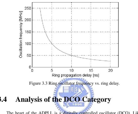
r consists of the propagation delays, rough the positive and negative edge in the ring. If the delay
The output period of the ring oscillato
th dringis assumed
of the ring oscillator is symmetric for both transitions, the frequency
1 2 ring ring f d =
This relationship is illustrated in Figure 3.3. The slop of the curve increases towards small ring delays. Even for very large rings with an oscillation frequency of 25 MHz, the slope at 25 MHz is approximately 1.25 kHz/ps or 50 ppm/ps. Applied to
a ring oscillator, this would require a delay resolution in the ring of 0.02 ps at 25MHz. Digital delay generation with such a high accuracy is not realistic. In Chapter 4, a method for improving the frequency resolution of all digital ring oscillators is proposed.
Figure 3.3 Ring oscillator frequency vs. ring delay.
3.4
Analysis of the DCO Category
The heart of the ADPLL is a digitally controlled oscillator (DCO). Like most voltage-controlled oscillators, the DCO consists of a frequency-control mechanism within an oscillator block. Generally speaking, an odd number of inverters connected ome a ring oscillator. The clock period of the ring oscillator is two time of the inverter ferent clock period. Besides, a variable number of inverters implement a
the ring oscillator. One is the propagation delay time of an inverter and another is the any designs of the DCOs that have been presented.
in a loop chain bec
times the circular loop delay time. Different propagation delay produces dif
variable delay. Therefore, there are two parameters to determine the clock period of
number of the inverters. In terms of tuning these two parameters, there are m
Standard cell based DCO Design
most ADPLL designs. The main advantage is that the oscillator can be implemented by standard-cell library.
Figure 3.4 A typical ring-oscillator.
The modified architecture is shown in Figure 3.5 [18]. The enable signal powers the ring-oscillator. The path selection consists of tri-state inverters. The path selections from p1 to p4 are used to select different delay time of ring-oscillator to change output frequency. The problem of the architecture is a large parasitic capacitance at node 1 in Figure 3.5, and the DCO resolution is poor due to no fine tune cell being applied.
Figure 3.5 Modified architecture in [18].
An improved DCO architecture is showed in Figure 3.6 [14]. It is separated into two stages: a coarse-tuning stage and a fine-tuning stage. To avoid large loading capacitance appearing in the path selection output, the path selector is partitioned into two stages. In the first stage, sixteen coarse-tuning delay blocks select a partial output. The second stage path selector will select the final output.
Figure 3.6 An improved DCO architecture in [14].
A cell-based digital controlled oscillator is shown in Figure 3..7[19]. It is a multiple path selection DCO with a delay matrix. When searching frequency, the path selection works as coarse search and the delay matrix works as fine search. The delay matrix consists of several parallel tri-state inverters. Its disadvantage is the large parasitic capacitance in the output node of the path selection.
Figure 3.7 Structure of the cell-based DCO in [19].
Another cell-based digital controlled oscillator is shown in Figure 3.8[20]. The oscillator being implemented is a seven-stage ring oscillator with one inverter replaced by a NAND gate for shutting down the ring oscillator during idle mode. To change the frequency of the ring oscillator, a set of 21 tri-state inverters are connected parallel to each inverter. When the tri-state inverters are enabled, additional current is added to drive each inverter stage. Although the DCO has the advantages of being made from all-standard cells, it has disadvantages such as relatively high power consumption and low maximum frequency from high capacitive load in the ring oscillator.
Figure 3.8 DCO using parallel tri-state inverters to adjust frequency in [20].
Delay cell DCO design
A DCO structure is showed in Figure 3.9(a) [12]. The ADPLL controls the DCO frequency through the DCO control word. Arithmetically incrementing or decrementing the DCO control word modulates the DCO frequency and phase. The magnitude of the incremental changes to the DCO control word defines the gain, which, in turn, dictates the relative change in DCO frequency(△F/△DCO control word). As Figure 3.9(a) shows, the requisite odd number of inverting stages in the DCO is obtained by using one enabling NAND gate and eight controllable cells. Figure 3.9(b) illustrates the basic premise of a constituent DCO cell. The sizing ratio ntrol devices is 2X to achieve binary weighted control. Hence, the DCO cell disadvantage is large area overhead.
of the co
can control the propagation delay time with n-bit control word. The the
Figure 3.9(a) 8-cell DCO with control bit [12].
Figure 3.9(b) Constituent DCO cell [12].
Another DCO structure is showed in Figure 3.10[16]. The DCO consists of four
he DCO cells work as the fine tune. The area of the DCO in Fi
paths and four DCO cells. The DCO cell is shown in Figure 3.9(b). The path selection works as the coarse search. T
gure 3.10 is smaller than the area of the DCO in Figure 3.9(a).
An improved DCO architecture is showed in Figure 3.11(a) [21].The DCO consists of coarse cell, fine cell, unit gain circuit and voltage divider. The DCO control word is the 8 binary weighted control signals. The weighted control signals DCO[4]~DCO[7] control the coarse cell and the others control the fine cell. The switch of the coarse cell is turned on by the Voltage_A and the switch of the fine cell is turned on by the Vdd voltage or Gnd voltage. By the two stage method, it can save
e area and power consumption. The coarse cell of the DCO was shown in the Figure _A becomes Vdd voltage or Gnd voltage.
th
3.11(b) . The fine cell is the same with coarse cell but the Voltage
Figure 3.11(a) An improved DCO architecture in [21].
3
Generation method equency range Frequency resolution Intrinsic Jitter All digital Circuit.5 Summary
Existent clock generation methods have been explained and the performance has been compared to the requirements mentioned above. Table 3.1 lists the characteristics of conventional clock generation circuits. In the next chapter, a new clock generation methods are proposed.
Table 3.1 Characteristics of various clock generation circuits. Clock
Fr
VCO high high low , depends on pull-range No , analog technique
VCXO very high high very low
No , analog technique Voltage controlled Ring Oscillator
high high low
No ,analog Ring delay control All digital Ring Oscillator
very high low low yes
Ch
ed Oscillator with
High Resolution and 8-Phase Output
4.1
uction
Traditional analog circuit design, such as voltage controlled oscillator (VCO), shifts the design paradigm towards more digitally intensive techniques. The digitally cillator is the key component of all digital PLL. The quality of the output clock is decided by its performance. There are three issues to design a DCO. First, the output clock of a DCO is discrete, so the resolution of a DCO should be sufficiently high to maintain acceptable jitter. Second, for searching target frequency and phase easily and efficiently. A DCO has better monotonic response to the DCO control word. Third, a DCO has better noise immunity, so the output clock will not induce large jitter. The noises come from power supply, control word transition, or other condition. Thus, this chapter attempts to propose a high resolution DCO by using transmission gates as novel delay cells.
apter 4
Digitally Controll
Introd
4.2
Basic Concepts of Digitally Controlled
s
Introduction to the fundamental function of DCO
lly on of a digital input word D, as follows:
Oscillator
The fundamental function of a DCO is to provide an output waveform, typica in the form of square wave. The square wave has a frequency f that is a functi
1 2 1 0 1 2 1 0 ( ) ( 2n 2n 2 2 ) DCO n n f f D f d d d d D C O − − − − = = Δ × + + ⋅⋅⋅ + +
Typically, the DCO transfer functionΔ ×f (dn−12n−1+dn−22n−2+ ⋅⋅⋅ +d121+d020) is defined so that either the frequency or the period of oscillation is linear with D, generally with an offset. For example, a DCO transfer function that is linear
frequency is typically expressed as:
D C O
f TD C O
in
( ) offset
f D = f +D⋅ Δf
Where: fo ffset is a constant offset frequency andΔ is the frequency quantization step. f
milarly, a DCO transfer function that is linear in period is typically expressed as: Si
( ) offset
T D =T +D⋅ ΔT
Where:To ffsetis a constant offset period andΔ is the period quantization step. It is T
converted the frequency directly to the digital value, and change the gain for VCO control adaptively. However, to design a high resolution DAC is extremely difficult. In addition, the VCO is an analog block that is easy to be influenced by power and substrate noise. The chip area cost is very high due to DAC evident that, since the DCO period ( )T D is a function of quantized digital input D. The DCO can not generate a continuous range of frequencies. In this regard, the quantization granularity of the DCO period sets some fundamental limits on the achievable jitter of an all digital PLL. It is of course desirable to have a fairly small quantization step size.
Analysis of the DCO Design Approaches
(1). The DCO constructed with the DAC and the VCO:
The DCO in [22] is directly utilized digital-to-analog converter (DAC) and conventional voltage controlled oscillator (VCO) as shown in Figure 4.1. Another DCO in Figure 4.2[23] is
and VCO.
Figure 4.1 The DCO constructed with the DAC and the VCO in [22].
Figure 4.2 The DCO constructed with the DAC and the VCO in [23].
(2). The DCO constructed with high speed clock and divider:
The common type of conventional DCO includes a high frequency oscillator in combination with a programmable frequency divider. Figure 4.3 shows the DCO. A programmable frequency divider receives an n-bit digital control word D which indicates the divisor values. The output DCO (CLK) signal is to be divided from a high speed oscillator (HFCLK).
The period quantization stepΔ is limited by the high frequency oscillator T
(HFCLK) in this arrang ent. Low jitter operation thus requires oscillator to operate at an extremely high frequency. For example, a 100 ps step between periods require high frequency oscillator and programmable counter to operate at 10GHz. This will consume a lot of power consumption.
em
Figure 4.3 The DCO constructed with high speed clock and divider.
(3). The DCO
Because of the speed limitation, other conventional DCO approaches directly synthesis a signal, rather than dividing down from a high frequency source. Figure 4.4 shows a variable length ring oscillator. For example, delay buffer are connected in series. A decoder decodes n-bit digital control word D into control lines. If the propagation delay time of each buffer stage is Tbuffer. Then the period quantization
step is thus 2*Tbuffer, which is typically an improvement over Figure 4.3’s design.
However, the period quantization step still may be too coarse for many applications. constructed with variable length ring oscillator:
2n
2n
Figure 4.4 The DCO constructed with variable length ring oscillator.
Enhance Fine Resolution of the DCO design
The basic skill to enhance the fine resolution of DCO is to enhance overall driving capability. The methods are to adjust the overall resistance (R), or to adjust capacitance (C), or to adjust inductance (L) as shown in Figure 4.5.
Figure 4.5 General mechanism for enhance of fine tune in the DCO. (1). The mechanism are to adjust the resistance:
As shown in Figure 4.6[24], the pull-down stack uses a transistor array in which multiple rows are allowed. The transistor array actually forms the digitally adjustable resistor. Each bit of the control signal b[n-1:0] is connected to the gate of one transistor in the array.
Figure 4.6 The mechanism are to adjust the resistance.
(2). The mechanism are to adjust the capacitance:
As put
ference of to build digitally controlled varac
shown in Figure 4.7[25], has developed a novel DCV using three-in NAND gates for DCO design. The DCV uses the gate capacitance dif
NAND gates under different digital control inputs
tors (DCV) as shown in Figure 4.7(a). Figure 4.7(b) shows the equivalent circuit of Figure 4.7(a), an initial capacitance (CI) parallels with a capacitance difference
with (ΔC). The D input controls the capacitance (ΔC) in the output (Out) node. The marked transistor (Mn2) produces a large capacitance difference under different D
states.
C
Δ
Figure 4.7 The mechanism are to adjust the capacitance.
Fine Tune in Standard Cell Design
For most digital applications, a standard cell description of the digitally controlled oscillation simplifies the design, and it can be easily ported to different processes in a very short time period.
The fine delay steps determine the resolution of the delay line. Three fine delay generation methods are illustrated in Figure 4.8, Figure 4.9, and Figure 4.10. The first
one consists of igure 4.8 [26].
ne of the buffers is loaded by a small capacitance, while the other is not. This results depends on the load and on the
can rari
a multiplexer and two identical buffers. As shown in F O
in a delay difference between the two paths Tfine that
drive strength of the buffers, but not on the absolute delays of the buffers. The minimum delay Tmin of this fine-delay line is the sum of Lfine. The Lfine is propagation
delays of all unloaded buffers with their corresponding multiplexers. In order to reduce the minimum delay, the buffer can also be replaced by inverters and non-inverting multiplexers by inverting multiplexers. Both inverting cells are signifi tly faster in most standard-cell lib es than their non-inverting counterparts.
Figure 4.8 a multiplexer and two identical buffers structure.
The second type shown in Figure 4.9 [27], depending on the technology above, replacing the multiplexers and the buffers by NAND gates can improve the minimum delay further. The main idea is using the delay different of paths. For example, the capacitances and output strengths of different pins are close for a NAND gate in standard-cell library. The timing delay difference from different input pins to the same output pin approximates to the intrinsic difference.
Figure 4.9 replace the multiplexers and the buffers by NAND gates.
The third type consists of a bank of tri-state buffers driving the same node. As shown in Figure 4.10[19]. The number of enabled buffers influences the delay of the cell. The frequency resolution is decided by the minimum scale of a delay matrix. It is important for systems not only to maintain a table clock but also to ensure minimum frequency error. In order to improve the linearity of the delay sequence, some buffers may drive permanently, and the increment of activated buffers may be not constant.
Figure 4.10 a bank of tri-state buffers.
Fine delay generation methods, the Figure 4.8 and Figure 4.9 solutions are based on two identical buffers with different loads. The Figure 4.10 uses the drive strength of a bank of tri-state buffers to control the delay.
Another e cell and
or-and-inverter(OAI) cell with two parallel tri-state inverters was proposed in Figure 4.11[
xample of DCO implement by an and-or-inverter(AOI)
14]. The basic method is to adjust the driving capability with resistance control. Its resolution step is non-uniform and sensitive to power-supply variation because it is based on AOI-OAI cell to change the delay resolution. In addition, this technique also requires an additional decoder for mapping AOI-OAI cell control inputs.
Figure 4.11 High resolution delay cell.
4.3
The Proposed Fine Tune Delay Cell with
High Resolution
The DCO with High Resolution Delay Cell
The proposed DCO, like most voltage controlled oscillators or delay control, employs a frequency control mechanism located inside an oscillator block. Two parameters are used to modulate the output frequency of a ring oscillator. Namely two parameters are the propagation delay time of each delay cell, and the total number of delay cells in the close loop. Thus, we developed a novel delay cell using transmission
gate in the fine tune ce O improves delay solution and demonstrates monotonic delay behavior with respect to digital control code
driving strength dynamically using a fixed
ll design of DCO. The proposed DC re
s.
Basically, two main techniques exist for design a fine resolution in DCO with shunt capacitor. One technique changes the MOS
capacitance loading and achieves a fine resolution [28]. Meanwhile, the other uses the shunt capacitor technique to fine tune capacitance loading and achieves high resolution [29]. Figure 4.12 shows the conventional control mechanism with the shunt capacitor circuit. In Figure 4.12, Mc serves as a capacitor. The gate of transistor Mctrl (Dctrl) controls the discharge current and charge current. Hence, Dctrl can control the delay resolution from In to Out.
Figure 4.12 Conventional control mechanism with shunt capacitor.
Thus in previous design, as shown in Figure 4.10, the delay matrix uses parallel buffers to enhance the resolution of the delay cell. However, the area cost and ption for the delay matrix is too large to be used in a low cost and tri-state
the power consum
low power design. As shown in Figure 4.11, its area cost and power consumption is low, the average resolution of the delay cell is about is 5ps.
The Proposed High Resolution Delay Cell
As mentioned before, there are two main techniques existing for design a fine resolution in DCO. However, the proposed a method of changing capacitor value to modulate frequency with fixed current value.
Figure 4.13(a) illustrates a novel delay cell using a transmission gate. The proposed method controls the capacitance between gate and source or between gate
and drain. In Figure 4.13(a), the gate capacitance of transmission gate at node CL depends on control nodeVfc ’s value. The total gate capacitance at node CLvaries withVfcinput states. Figure 4.13(b) shows the equivalent circuit of Figure 4.13(a), an initial capacitance (C ) parallels with a capacitance difference I
(ΔC). TheVfcinput controls the capacitance (ΔC) in the output (Out) node.
C Δ
Figure 4.13 Proposed delay cell with transmission gate. (a) Circuit with digital control. (b) Equivalent circuit with ΔCcapacitance.
“off ”. As Figure 4.14(b) shown, the capacitance value of
Figure 4.14 shows the gate capacitance difference characteristic which is simulated using the Hspice circuit simulator. Figure 4.14(a) shows the gate capacitance of transmission gate when the mp and the mn is “on” or “off ”. Figure 4.14(b) illustrates the gate capacitance of the mp and the mn when them is “on” or
C
Δ is estimated at “fF” ated at s” grade.
grade. As described in [30], the transmission gate equivalent resistance is estim “k-ohm” grade. Therefore, theΔTcan be achieved “p
Cp(on)
Cn(on)
Cp(off) Cn(off)
Figure 4.14(a) The gate capacitance of transmission gate.
Cp+Cn(on)
Cn+Cp(off)
ΔC
Figure 4.14(b) The gate capacitance of transmission gate.
Figure 4.15 illustrate the difference of equivalent capacitor value from drain with OS “on” or “off ” to modulate high timing resolution. When MOS is “on“, the M T Δ =R*ΔC Æ (ps = kΩ*fF) Gate voltage (V) Gate voltage (V) Gate capacitance (fF) Gate capacitance (fF)
equivalent capacitor value from drain will be larger. When MOS is “off “, the quivalent capacitor value fr rain a ssume the fine-tune section has a 6-bit control word and adopt a binary weighted control mechanism.
e om d will be sm ller. A
Figure 4.15 High resolution delay cell.
Figure 4.16 illustrate the high ell simulation result. Fine-tune
input control wo 4 different
delays can be provided. In this simulation, the average resolution is about 125.7fs = [8.05ps/64]. In the versus control word is very linear. For gigabit optical communication, this resolution is quiet sufficient.
resolution delay c
rd rang from “000000” to “111111”. Thus, a total of 6
meantime, delay time
4.4
Structure of the Proposed DCO
Structure of the DCO and Design Guide
This DCO design applications demand high resolution, high speed, and multi-phase output. Namely, the design target is 1.25GHz, 8-phase output, and high resolution. As shown in Figure 4.17, the DCO is consisted of four delay elements (DCO-cell) with differential operation frequency and 8-phase output. The oscillation frequency depends on the equivalent load resistance and equivalent capacitance of the delay element. By tuning the equivalent capacitance can obtain the desire oscillation frequency. In the test chip, the DCO is implemented with TSMC 0.18um 1P6M CMOS process.
Figure 4.18 illustrates the structure of the proposed cell-based DCO-cell with
10-bits binary weighted c re is separated into
ree stages, the coarse-tuning stage, the medium-tuning stage and the fine-tuning stage
x structure, whose characteristics are determined by both the combination and number of tri-state inverters. Note that the dynamic control range is determined by the combination of tri-state inverter matrix.
The medium-tuning stage is consisted of three proposed hysteresis delay cell (HDC). The HDC contains two tri-state inverters. The operation concept of HDC is to control driving current to obtain different propagation delay. When tri-state inverter of HDC is enabled, the output signal of enable tri-state inverter has the hysteresis phenomenon in the transition state to produce different delay times from the delay chain. As shown in Figure 4.18, addition to the latch between two signal paths. The latch is consisted of two minimum size inverters. The way of adding small latch forces two signal paths differential is called “pseudo-differential”. Both side of latch will force two signal paths to be 180 degree out of phase.
In order to ng delay cells
re added. The fine-tuning stage is consisted of four transmission gates. The circuit of ontrol. The proposed DCO-cell structu
th
. Besides, the DCO-cell still contains the trigger circuit, as shown in Figure 4.19. The higher three bits of the control code are for coarse-tuning stage. The lower four bits of the control code are for fine-tuning stage. Other three bits of control code are for medium-tuning stage. The coarse tuning stage is consisted of an always on of tri-state inverter and three tri-state inverters. It is a matri
increase frequency resolution of the DCO, the fine-tuni a
fine-tuning delay cell is shown in Figure 4.13(a). The detail information about how to esign the fine-tuning delay cell is discussed in Section 4.3.
d
Figure 4.17 The proposed DCO architecture.
Figure 4.18 The proposed DCO-cell architecture.
Design of the DCO
The minimum required voltage gain and contributed phase shift per stage are erived based on “Barkhausen criteria”. Thus, we analyze the DCO from the small-signal model. Figure 4.20 illustrates the small-signal model of the DCO-cell structure. Figure 4.21 represents the parameters including the transconductance, the output impedance, and the output capacitance of the coarse stage, the medium stage, and the fine stage.
d
Figure 4.20 The small-signal model of the DCO-cell.
Figure 4.21 The parameter of the DCO-cell
The small-signal model equation derived from Figure 4.20 is shown as follows
[ ] [
[ ] [
out out
mm outb mc inb Lc Lm f out oc om outb outb mm out mc in Lc Lm f outb oc om v v g v g v SC SC SC v R R v v g v g v SC SC SC v R R ⋅ + ⋅ + + = − + + ⋅ ⋅ + ⋅ + + = − + + ⋅ ] ] The transfer function of the DCO-cell(H s( )) is shown as follows
( ) ( ) 1 1 ) ( mm Lc Lm s g S C C C R R − + + + + + ( ) o mc i f oc V s g H s V = = (1)
where is the transconductance of the coarse stage; is the transconductance
om mc
of the medium stage; Rocis output impedance of the coarse stage; Romis output impedance of the medium stage; CLcis load capacitance of the coarse stage; CLmis load capacitance of the medium stage; Cf is equivalent capacitance of the fine stage. The transfer function of each stage denotes 0
0 (1 ) A S ω +
. Hence the loop gain of the
four stages is 4 0 0 4 ) A H s S ω + (
Equation (3) can be derived from equations (1) and (2): ( ) (1 = 2) 4 [ gmc ] + 4 1 1 ( ) ( ) ( ) [1 ] 1 1 ( ) mm oc om Lc Lm f mm oc om g R R H s S C C C g R R − + = + + + − + + (3)
The 3-dB bandwidth of each stage can be derived from equation (3):
0 1 1 ( ) ( ) mm oc om Lc Lm f g R R C C C ω − + + = + + (4) For the circuit to oscillate, each stage must contribute a frequency-dependent phase shift of180 45
4
°
= . The oscillating frequency is given bytan 1
0 45 osc ω ω − = ° . Hence osc
ω is equal toω0. The minimum voltage gain of each stage can be derived as follows 2 0 1 1 ( ) 1 1 (ω ) mc mm oc om osc g g R R ω − + + = + (5)
The minimum voltage gain of each stage can be derived from equat as
ions (2) and (5)
0 2 A = .
h
( H j( ωosc) =1)”. This is 2 1 1 2 mc mm oc om osc R R ω = (6) 2 ( ) ( Lc Lm f) g g C C C − − + + + +
From equation (6), the oscillation frequency of the ring oscillator can be derived:
2 2 2 1 1 ( ) 1 2 ( ) mc mm oc om osc Lc Lm f g g R R f C C C π − − + + = + + (7) From equation (7), the maximum oscillating frequency ( fmax) and the minimum oscillating frequency ( fmin) can be derived as follows:
max: f mm(min) 1 1 oc om g R R ≅ + Æ max 1 (max) 2 ( ) mc Lc Lm f g f C C C π ≈ ⋅ + + (8) min : f mm(max) 1 1 oc om g R R >> + Æ 2− 2 (min) (max) min 2 1 2 ( ) mc mm Lc Lm f g g f C C C π ≈ ⋅ + + (9) as follows:
From equations (8) and (9), the operating frequency range ( frange) can be derived
(min) (gmm(max) 2) ] (10) 2 max (max) (max) [1 ( mc ) range mc mc g f f g g ≈ ⋅ − −
ratio of the coarse stage and the medium stage (
From (10), 50% frequency-tuning range can be achieved with a transconductance mm
mc
g
g ) being 6 /13 .
is of the DCO
There are two issues in designing the desired DCO; a sufficiently high resolution to maintain acceptable jitter, a monotonic response of the control word to the oscillation frequency, and high noise immunity.
The clock period control range of the DCO consists of several sections. The
trol ran ust be larger than the clock period difference between each two neighbor control words. Otherwise, there are frequency gaps in each two neighbor
Analys
control range of each control word determines the clock period of each section. The
control words. Moreover, in order to increase the tolerance of the process variation, the overlap of the clock period must be large enough.
This basic concept of the clock control period range is illustrated in Figure 4.22. Having these basic concept and design issues, we can design the DCO in detail based on above discussions.
Figure 4.22 Influence of PVT variations on the controllable frequency range.
n Results and Layout
ent corner cases. As shown in Figure 4.23
4.5 Simulatio
Follow the methods in Section 4.3 and Section 4.4, we propose the DCO architecture as Figure 4.17, Figure 4.18, and Figure 4.19. Figure 4.23 illustrates the clock period of the proposed DCO at three differ
796.01p 1077.5p 678.01p 901.28p 593.63p 802.61p 779.03p 811.96p Tuning Range of 3 Corner Cases Chain
C loc k P er io d of D C O Coarse Code
Figure 4.23 The clock period range of the DCO at three different corner cases.
Figure 4.24 shows monotonous curves of tuning code according to medium tuning frequency of the DCO at TT corner.
778.67p
806.09p
798.04p
801.99p Tuning Range of Medium tune Chain
Cloc k P er i C O o d of D Medium Code
Figure 4.24 Tuning range of medium stage.
Figure 4.25 shows monotonous curves of tuning code according to fine tuning frequency of the DCO at TT corner. And delay range of the fine tune chain is about 6.07ps. Therefore, the average resolution is about 0.38ps.
798.04p
800.09p
804.11p Tuning Range of Fine tune Chain
C loc k P er io d o f D C O Fine Code
Figure 4.25 Tuning range of fine stage.
Gap issue
In order to consider period gaps in each two neighbor control words, the gaps issue is analyzed. As shown in Figure 4.26(a) and Figure 4.26(b), period in each two neighbor control words are overlapped at TT corner. Thus, the proposed DCO has no period gaps in each two neighbor control words.
Figure 4.26(a) The coarse-code vs. medium-code period overlap diagram.
Figure 4.26(b) The medium-code vs. fine-code period overlap diagram.
Table 4-1 shows the form of period overlap at three different corner cases. As shown in Table 4-1, the periods in two neighbor control words are overlapped at three different corner cases. Thus, the proposed DCO has no period gaps in each two neighbor control words at three different corner cases.
Table 4-1 The form of period overlap.
Layout
The digitally controlled oscillator is implemented in TSMC 0.18μm 1P6M CMOS process. The layout of this chip is shown in Figure 4.27. The core area is
“ 310um×220um ”, while the chip area is” 680um×680um ”. The post-layout simulation result summary is shown in Table 4-2.
Figure 4.27 The layout of the proposed lled oscillator.
Table 4-2 The summary of the performance digitally contro
4.6 Comparisons and Summary
omparisons
Table 4-3 shows the comparisons among different DCOs. As shown in Table 4-3, the proposed DCO with multi-phase output achieves the finest LSB resolution.
Table 4-3 Comparison with existing DCOs.
C
Summary
Table 4-3 shows the comparisons among different DCOs. As shown in Table 4-3, the proposed DCO with multi-phase output achieves the finest LSB resolution.
In this chapter, the basic DCO concept, the basic DCO design, and fine tune methods are discussed at first. Then, a digitally controlled oscillator with 8-phase output using the transmission gate as digitally controlled fine-tune cell is presented. The proposed DCO is implemented in TSMC 0.18μm 1P6M CMOS process. It can be operate from 1.06GHz to 1.5GHZ. The average delay resolution of the DCO is 0.38ps. The proposed DCO has multi-phase output, high resolution, and small silicon area suitable for high-speed serial link application.
Chapter 5
Conclusions
5.1
Conclusions
oposed a digitally controlled oscillator has high timing resolution, and
.5Gb/s
t
DCO oscillating frequency slightly. he DCO timing resolution can be improved to about 0.38ps by adding fine-tuning delay stage. The frequency range is about 1.06GHz to 1.5GHz by HSPICE circuit simulation. The proposed digitally controlled oscillator circuit is designed using TSMC 0.18
This thesis pr
multi-phase output (8-phase) for ADPLL. The proposed digitally controlled oscillator can be applied to “a 1.25GHz ADPLL with 8-phase output” and “a 2
data-transceiver architecture”. Thus, there are two issues in designing the desired DCO; a sufficiently high resolution to maintain acceptable jitter, a monotonic response of the control word to the oscillation frequency. As the simulation results in Section 4.5, the proposed DCO can achieve the targe on above discussions.
The digitally controlled oscillator circuit is consisted of four delay elements (DCO-cell) with differential operation frequency and 8-phase output. This thesis proposes a novel fine-tuning method to change the
T
![Figure 2.7 shows the ADPLL with fixed high speed clock and accumulator in [15].](https://thumb-ap.123doks.com/thumbv2/9libinfo/8011401.160464/19.892.141.760.391.724/figure-shows-adpll-fixed-high-speed-clock-accumulator.webp)
![Figure 2.9 Function block of ADPLL in [14].](https://thumb-ap.123doks.com/thumbv2/9libinfo/8011401.160464/21.892.176.729.549.776/figure-function-block-adpll.webp)
![Figure 3.10 Structure of DCO in [16].](https://thumb-ap.123doks.com/thumbv2/9libinfo/8011401.160464/30.892.223.728.131.733/figure-structure-of-dco-in.webp)
![Figure 4.1 The DCO constructed with the DAC and the VCO in [22].](https://thumb-ap.123doks.com/thumbv2/9libinfo/8011401.160464/35.892.272.688.167.463/figure-dco-constructed-dac-vco.webp)
