國
立
交
通
大
學
光電工程研究所
博 士 論 文
低溫氧化物半導體及有機半導體之電晶體及感測器研究
Low Temperature Transistors and Sensors based on Oxide
Semiconductor and Organic Semiconductor Materials
研 究 生:蔡武衛
指導老師:冉曉雯 教授
低溫氧化物半導體及有機半導體之電晶體及感測器研究
Low Temperature Transistors and Sensors based on Oxide
Semiconductor and Organic Semiconductor Materials
研 究 生:蔡武衛 Student: Wu-Wei Tsai
指導老師:冉曉雯 Advisor: Hsiao-Wen Zan
國立交通大學
光電工程研究所
博士論文
A Dissertation
Submitted to Institute of Electro-Optical Engineering National Chiao Tung University
in partial Fulfillment of Requirements for the Degree of
Doctor of Philosophy in
Electro-Optical Engineering November 2011
Hsinchu, Taiwan, Republic of China
I
低溫氧化物半導體及有機半導體之電晶體及感測器研究
研究生:蔡武衛 指導教授:冉曉雯 博士
國立交通大學光電工程研究所
摘 要
軟性電子與顯示器的開發在近年來是新世代在電子領域之研究的重要方針, 目前具有潛力的電晶體如有機半導體電晶體與無機氧化物半導體電晶體,兩者相 較於傳統非晶矽(a-Si)電晶體元件有以下幾項優勢,如較低的製程成本及較低製 程溫度(<200℃),且易於大面積液態製程,所以近年來被許多專家學者廣泛的研 究及探討。然而,後者的載子遷移率相較於前者具有更好的表現,所以在應用層 面上較為廣泛如在高頻電路上等。 首先,在論文第二章節裡,提出一個簡易的製程技術,在元件的通道做處理, 製作出許多的短通道,且利用電漿處理大幅提通道與通道間的載子濃度,進而改 善元件的載子遷移率從 4 到約 80 cm2 /V s。相較於傳統的銦化鎵氧化物半導體, 大多數的研究都是利用電漿處理元件的源極及汲極介面,以去降低元件的接觸電 阻,進而提升元件的特性,且一般傳統的載子遷移率往往都是小於 40 cm2 /V s, 除了一些研究團隊利用一些特殊的技術,如雙層的氧化物半導體層(IGZO/ITO), 或是利用高介電常數(Ta2O5)的絕緣層,去提升元件的載子遷移率為 60~100 cm2 /V s。在此,我們的研究中也討論到奈米點摻雜的數量以及電漿處理的時間都會 影響到元件的特性。由於元件目前製程尚未把元件封裝,且通道孔洞化的結構 受到外界水、氧分子的影響使得元件的穩定性較差,未來我們會覆蓋保護層 (passivation layer)於元件之通到處,且期望搭配一些規則陣列的圖案取代現有的 製程技術,以達到元件的最佳特性。在本論文中,我們也討論到了有機光(章節 三、四)和氣體感測器。此兩種光的偵測器,如光偵測器二極體及光偵測器電晶 體,在章節三提到的光偵測器二極體中,我們首先發現,垂直式元件於垂直方向 的載子遷移率會影響元件對光偵測的頻寬的大小,在此我們利用富勒烯(C60)當 作光偵測器的受體(acceptor layer),並改變元件在垂直方向的電洞之載子遷移率 從 2.3×10⁻⁵ 到 2.8×10⁻⁴ cm2 /Vs,可以提升元件偵測的頻寬從 10 到 80 MHz(元 件的操作偏壓為 4 伏特)。本論文在第三章節有詳細的討論。另外,在章節四提 到的垂直式光電晶體上,為了方便光載子的拆解,我們將我們現有的(p-type)垂 直式電晶體中摻雜少許的(n-type)材料,且在照光下的反應,我們發現外部量子 效率(EQE)可以提升至 360%在 620 奈米下。在此,我們推斷為元件在照光下屏 蔽了基極的控制所以大幅提升 EQE,且本論文在第四章節有進一步的討論 。最 後,在氣體感測器上,在本論文第五章節裡有討論到利用水平式並五苯環II (pentacene)有機薄膜電晶體當作氨氣感測器,我們在此利用紫外光(UV)處理元件 的絕緣層(PMMA),為了去修飾絕緣層表面的形成氫氧官能基進而提升元件的反 應靈敏度,且在有處裡的絕緣層最低可以偵測到的氨氣濃度為 0.5ppm。此偵測 的 範 圍剛 好可 以 判斷一 般 病人 是否 患 有肝病 ( 健 康病 人呼 出的氨 氣 含量 為 0.745ppm;肝硬化病人呼出的氨氣含量為 0.278ppm)。因此非侵入式有機電晶體 當氣體感測器在未來電子產品的發展是相當具有潛力的。本論文最後章節為垂直 式有機電晶體的開發,此項工作為本人與趙宇強博士、陳俊宇博士、姜鈞銘、姜 淑玲、古明哲共同完成,垂直式有機電晶體相較於傳統的水平結構電晶體有幾項 優勢:(1)可以不利用到黃光微影技術就能使通道長度縮至小於 1(微米)等級,(2) 低的操作電壓,(3)高輸出電流。在此章節裡,我們有改變不同的半導體材料製 作不同的空間電荷限制垂直式電晶體,並探討其工作原理與元件特性。在我們的 研究之中,高分子垂直式電晶體具有較好的操作特性,如其操作電壓在為 1 伏特 下最大輸出電流為 0.14 mA/cm2,元件的開關比為 24310,電流增益為 104個數量 級,另外我們的半導體層也有嘗試利用蒸鍍的方式成膜,但得到的成果不盡理想, 再本論文中會再加以討論其原因。
III
Low Temperature Transistors and Sensors based on
Oxide Semiconductor and Organic Semiconductor
Materials
Student : Wu-Wei Tsai Advisor : Dr. Hsiao-Wen Zan
Institute of Electro-Optical Engineering
National Chiao Tung University
ABSTRACT
The development of flexible electronics and displays are crucial for next generation electronics. Metal-oxide thin-film transistors (TFTs) and organic TFTs have higher potential than a-Si TFTs because of the following advantages:1) low-cost; 2) solution fabrication process on a large area array system; 3) low fabrication temperature (< 200 ℃); and 4) the applications are on a flexible substrate.
In the Chapter 2 of this dissertation, we proposed a high performance amorphous In-Ga-Zn-O (a-IGZO) thin film transistor with nano-dot doping (NDD). The nano dot structure creates many short channel and high concentration region in the channel region. Also, the performance of a-IGZO TFT can be controlled by the dots concentration and the Ar plasma treatment time. The proposed nano-dot doping reduces the effective channel length, lowers down the energy barrier, and enhances the effective field-effect mobility 19 times larger than that of the control sample without NDD. The proposed device is promising for the development of low-cost, lithography-free, and high-performance flexible electronics. In the Chapter 3 and
Chapter 4 of the dissertation, we introduce the two organic photodetectors, including
photodiode and phototransistor. In the Chapter 3, bilayered organic photo diodes with controllable carrier mobility in the p-type donor are demonstrated. Vertical carrier mobility of pentacene is demonstrated to be increased while the deposition rate is high. With C60 as the acceptor material and pentacene deposited at high deposition rate as donor material, the detection of 80-MHz signals is demonstrated. Using high mobility pentacene in stead of poly(3-hexylthiophene) (P3HT) to serve as the hole transport layer effectively improves the hole mobility over 1 orders and hence enlarges the operation bandwidth. The results enable the development of low-cost large-area organic image sheets for the detection of high-frequency signals. In the Chapter 4, we introduce a vertical polymer phototransistor with low operational voltage (-1.5 V). A blended polymer layer with both acceptor and donor materials was used as a
IV
channel material in the vertical space-charge-limited transistor (SCLT). Under illumination, we obtained external quantum efficiency (EQE) as high as 360% at 620 nm. We propose the effects of base-field shielding as a means to explain high EQE. This proposition has been supported by two-dimensional simulation of the device. Moreover, we also study the pentacene-based organic thin film transistor (OTFT) as ammonia sensor in the Chapter 5 of this dissertation. Non-invasive ammonia sensors are attractive alternatives for the diagnoses of a variety of chronic diseases such as liver cirrhosis and renal failure. A low cost pentacene-based organic thin film transistor (OTFT) fabricated by a novel and simple process was demonstrated to be highly sensitive and specific for ammonia gas. Various measurement parameters that reflected OTFT device characteristics for ammonia detection were investigated. Significant variations of the turn-on current, intrinsic mobility, and threshold voltage (Vth) were observed while subthreshold swing (S.S.) was almost unchanged to the
alteration of ammonia concentration. The OTFT device detected 0.5~5 ppm concentration ammonia gas at room temperature, which is in the critical range that can distinguish between healthy person and patients with liver cirrhosis and renal failure. The sensitivity of the device was further enhanced following a simple UV irradiation treatment to modify the functional groups on poly(methyl methacrylate) (PMMA) dielectric layer. Possible interference for ammonia detection such as humidity effect and selectivity among nitrogen, alcohol, carbon dioxide, acetone, methane and ammonia were also examined. We concluded that the proposed pentacene-based OTFT is a promising device for the future application in non-invasive medical diagnoses. In the Chapter 6 of this dissertation, an organic vertical transistor is investigated. In this work, I was cooperating with Dr. Yu-Chiang Chao, Dr. Chun-Yu Chen, Shu-Ling Jiang, Chun-Ming Chiang, and Ming-Che Ku. In the Chapter 6, the operation mechanism of vertical transistor is introduced. The turn-on current, on-off current ratio, current gain, and operation voltage of P3HT-based vertical transistor is 0.14 mA/cm2, 24310, 104, and 1 V. In order to improve the controllability and solve the accumulation of polystyrene spheres problems, the nano-imprint technology is used to replace the polystyrene spheres fabrication process and to from the grid structure.
V
Acknowledgement
能夠順利完成學業是令人開心的一件事情,碩博這五年多以來讓我學會了很 多解決事情的能力,且這一路走來要感謝非常多人的幫助。首先,我要感謝我的 指導老師冉曉雯老師,您處理事情的細心以及面對解決分析實驗上問題的能力, 真是令我非常欽佩以及是需要學習的地方;也要感謝孟心飛老師、洪勝富老師、 蔡娟娟老師在實驗上給予我很多的意見及支持,讓我的博士研究能夠更加的完整。 另外要感謝實驗室學長國錫、志宏、育敏、文馨、光明、廷遠、皇維、德倫、睿 志、芸嘉、宇強、士欽,給予我很多研究上的意見,且當我在面臨困難的時候, 你們都很樂意幫助我開導我讓我度過種種難關,希望你們未來都會非常順遂。也 要感謝當初一起修課努力的同學們,權陵、俊傑、志宇、旻君、和璁,謝謝你們 讓我的學生生涯更加地多采多姿,也希望你們的工作能一切順利。此外要感謝當 初與我一起熬夜打拼準備資格考試的伙伴,上傑、凌嶢。還要感謝實驗室可愛的 學弟妹們:感謝長紘,常常陪我一起聊天,祝你發表 Science 的夢想能夠實現; 感謝鈞銘、淑玲、玉玫、明哲,當初一起努力打拼分享實驗心得,也恭喜你們都 已順利畢業找到很好的工作;感謝家新,跟我一起努力奮鬥,讓我博士生涯畫下 完美的句點,也希望你在海陸部隊一切都能夠順利、平安;感謝王辰、培修,你 們的搞笑,真是實驗室的開心果;此外也希望認真的洪正、凱瑞、季遠、永軒、 建豪、茂家等實驗室所有成員們,祝你們都能夠順利畢業。也感謝助理明嬿、欣 鳳,幫忙處理實驗室大小事務,你們真的辛苦了,謝謝。也要謝謝我的女友蚊子, 常常聽我訴說我的實驗上的甘苦談,有了妳的傾聽,也讓我減輕了很大的壓力, 真是謝謝妳了。最後我要感謝我最親愛的父母,蔡日通先生、宋秋琴女士,給予 我最大的支持,在我幾次挫折時,都能給我很大的力量讓我有勇氣繼續走下去, 使得能夠成就今日的我,真是謝謝您們了。VI
Table of Contents
Chinese Abstract ... I English Abstract ... III Acknowledgement ... V Table of Contents ... VI List of Figures ... IX List of Tables ... XIV
Chapter 1. Introduction ... 1
1.1. Overviews of Metal-Oxide Semiconductor ... 1
1.1.1. Fundamental Transport Mechanism of Metal-Oxide Semiconductor ... 2
1.1.2. Oxygen Vacancy on a-IGZO Films ... 3
1.1.3. Argon Plasma Treatment on a-IGZO Films ... 4
1.2. Overviews of Organic Semiconducting Materials ... 5
1.2.1. Polymers ... 6
1.2.2. Small molecular weight materials ... 9
1.3. Overviews of Organic Sensors ... 11
1.3.1. Organic Photodetector ... 11
1.3.2. Ammonia Sensors ... 14
1.4. Overviews of Organic Transistors ... 19
1.4.1. Organic Field-Effect Transistors ... 19
1.4.2. Organic Vertical Transistors ... 22
Chapter 2. Effective Mobility Enhancement by Using Nanometer Dot Doping in amorphous IGZO Thin-Film Transistors ... 37
2.1. Introduction ... 37
2.2. Experiment ... 38
2.2.1. Device Fabrication Process ... 38
2.3. Results and Discussions ... 43
2.3.1. The Resistivity Variation of a-IGZO Thin Film after Ar Plasma Treatment .... 43
2.3.2. The Influence of Ar Plasma Treatment Time on a-IGZO TFT ... 46
2.3.3. The Influence of Dots Concentration on a-IGZO TFT ... 49
2.3.4. The Plausible Mechanism of Increased Mobility... 53
VII
Chapter 3. Increasing Organic Vertical Carrier Mobility for the Application
of High Speed Bilayered Organic Photodetector ... 64
3.1. Introduction ... 64
3.2. Experiment ... 65
3.2.1. Device Fabrication Process ... 65
3.2.2. Measurement Instrument ... 68
3.3. Results and Discussions ... 68
3.4. Conclusion ... 76
Chapter 4. Vertical Polymer Phototransistor featuring Photomultiplication due to Base-field Shielding ... 79
4.1. Introduction ... 79
4.2. Experiment ... 80
4.2.1. Device Fabrication process ... 80
4.2.2. Illumination System ... 85
4.3. Results and Discussions ... 86
4.4. Conclusion ... 97
Chapter 5.Pentacene-based Organic Thin Film Transistors for Ammonia Sensing ... 100
5.1. Introduction ... 100
5.2. Experiment ... 102
5.2.1. Device Fabrication Process ... 102
5.2.2. Gas Sensing System ... 104
5.3. Parameter Extraction ... 106
5.3.1. Field Effect Mobility ... 106
5.3.2. Threshold Voltage ... 107
5.3.3. Subthreshold Swing ... 107
5.4. Comparisons of Ammonia-Sensing Phenomenon in STD-OTFTs and UV-OTFTs ... 108
5.4.1. Electrical Properties of STD-OTFTs and UV-OTFTs ... 108
5.4.2. Gas Diffusion Model ... 110
5.4.3. Ammonia Concentration Effect ... 114
5.4.4. Sensing Phenomenon of UV-OTFTs ... 115
VIII
5.4.6. Phenomenon of Recovery ... 119
5.4.7. Humidity Effect ... 120
5.5. Conclusions ... 122
Chapter 6. Low Operated Polymer Vertical Transistors with High On/Off Current Ratio ... 128
6.1. Introduction ... 128
6.2. Experiment ... 130
6.2.1. Device Fabrication Process ... 130
6.3. Result and Discussions ... 135
6.3.1. Dielectric Characteristics ... 135
6.3.2. Output Current Characteristics of SCLT ... 135
6.3.3. Operation Mechanism of SCLT ... 141
6.3.4. Morphology Effect on Grid Structure ... 146
6.4. Conclusion ... 147
6.5. Future Work... 147
Chapter 7. Summary and Future Work ... 154
Vita ... 160
Publication lists ... 161
IX
List of Figures
1.1 The carrier transport paths in covalent semiconductors... 2
1.2 The carrier transport paths in amorphous oxide semiconductors. ... 3
1.3 Molecular structure of widely used conjugated polymers. ... 8
1.4 Molecular structure of widely used small molecular weight materials. ... 10
1.5 The operation mechanism of photo diode. ... 12
1.6 (a) The current density as a function of voltage (J-V), inset of Figure 1.7(a) is the device structure. (b) The frequency response of device... 13
1.7 Schematic of the bottom-gate organic field-effect transistors with (a) top contact or (b) bottom contact structures. (c) Schematic diagram of a (c) top-gate with bottom contact transistor using a standard TFT device structures. ... 20
1.8 Molecular and crystallographic structures ... 22
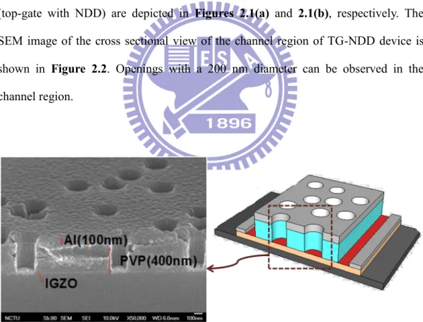
2.1 The schematic device structures of (a) STD (standard) and (b) NDD (nano-dot doping) top gate (TG) a-IGZO TFTs. ... 39
2.2 The SEM image of the cross sectional view of the TG-NDD a-IGZO TFTs in the channel region. ... 39
2.3 (a) The processes flow of the TG-NDD (top-gate with nano-dot doping) a-IGZO TFT. The SEM images of the PVP substrate adsorbed with (b) 0.2 wt % and (c) 0.8 wt % polystyrene spheres. The diameter of the sphere is 200 nm. By counting the PS spheres on SEM images in Figures 6.3(b) and 6.3(c), the concentration of dots per area is estimated to be 6.8106 mm-2 for 0.8 wt % PS spheres and is 4.8106 mm-2 for 0.2 wt % PS spheres, respectively. ... 42
2.4 Resistivity of the a-IGZO thin film as a function of the Ar plasma exposure time.. ... 44
2.5 (a) and (b) are O1s XPS spectra for IGZO without and with Ar plasma treatment films, respectively.. ... 45
2.6 The transfer characteristics of TG-STD devices with different Ar plasma treatment time on source/drain electrodes.. ... 47
2.7 The transfer characteristics of TG-NDD devices with high density dots (0.8 wt % PS spheres) with different Ar plasma treatment time. ... 48
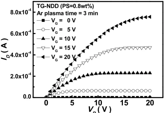
2.8 The output characteristics of TG-NDD devices (PS spheres: 0.8 wt %) with the optimal Ar plasma treatment time (3 mins). ... 49
2.9 The transfer characteristics and the root square of the drain current plotted as a function of gate bias for three devices: ... 50
X
structure in reference 13... 52
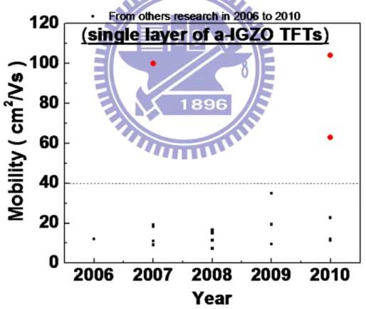
2.11 Effective field-effect electron mobility of this work and of other reports from 2006 to 2010. ... 52
2.12 The SEM images of different dots concentration. ... 54
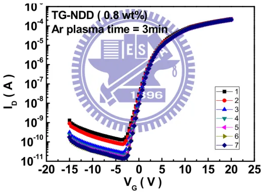
2.13 The transfer characteristics of TG-NDD devices when we repeating the measurement for seven times. ... 56
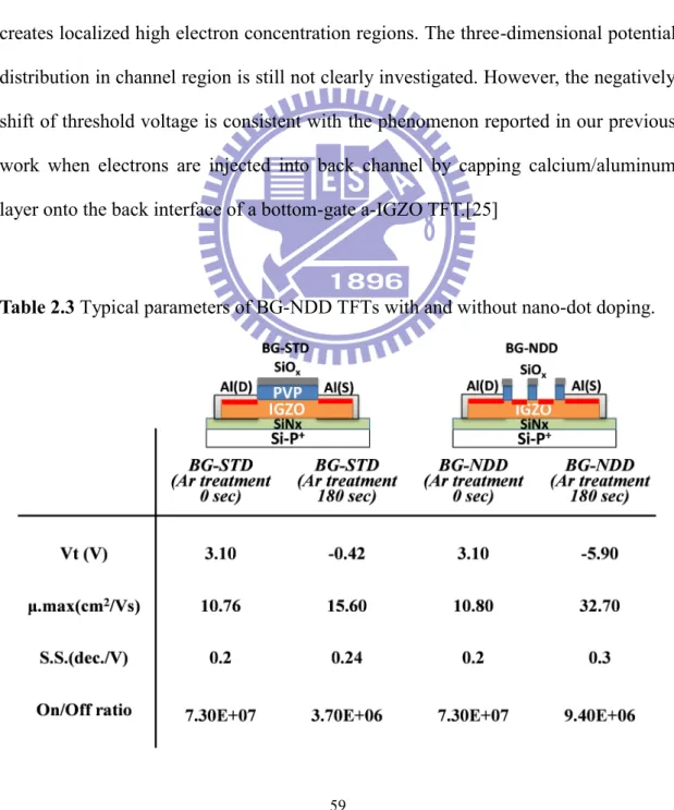
2.14 The schematic device structures of (a) standard (STD) and (b) nano-dot doping (NDD) bottom gate (BG) a-IGZO TFTs. (c) Four typical parameters (threshold voltage, on/off ratio, mobility, and subthreshold swing) of BG-STD and BG-NDD devices are extracted and plotted as a function of Ar plasma treatment time. ... 58
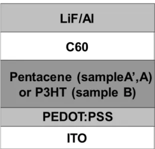
3.1 Schematic device structure of the bilayered photodetector.. ... 66
3.2 The energy band diagrams of sample A and sample B under reverse voltage biases.. ... 69
3.3 The incident photon-to-electron conversion efficiency of sample A and sample B under various reverse voltage biases... 69
3.4 The absorption spectra of pentacene and P3HT. The thickness of pentacene and P3HT is 100 nm. ... 69
3.5 The current density–voltage characteristics of organic diodes with C60, P3HT, pentacene deposited at 0.1 Å/s, and pentacene deposited at 1 Å/s. ... 70
3.6 The electrical frequency responses of pentacene diodes and P3HT diode.. ... 71
3.7 The rectifier circuit ... 71
3.8 The frequency characteristics of PDs made by pentacene and P3HT. ... 72
3.9 The schematic measurement setup.. ... 73
3.10 AFM images of 100 nm, 1.5 nm, and 3 nm pentacene films deposited at (a) 0.1 Å/s and (b) 1 Å/s, (c) 0.1 Å/s and (d) 1 Å/s, and (e) 0.1 Å/s and (f) 1 Å/s on PEDOT:PSS covered ITO glass, respectively. ... 75
3.11 X-ray diffraction (XRD) pattern of pentacene deposited on ITO surface. ... 76
4.1 Schematic illustration of the structure of P3HT or P3HT:PCBM-SCLT. ... 80
4.2 The defined emitter pattern with the ITO electrode. ... 81
4.3 The chemical structure of insulator (a) PVP (poly(4-vinylphenol)) cross-linked with (b) PMF (poly(melamine-co-formaldehyde) methylated). ... 82
4.4 The scanning electron microscopy (SEM) image when the PS is removed by the tape. ... 83
4.5 The PVP at sites without Al coverage were removed through plasma treatment of 150 W O2 for 13 min to open the channel region. ... 83
4.6 The chemical structure of (a) Polythiophene (P3HT) and (b) Phenyl-C61-butyric acid methyl ester(PCBM). ... 84
XI
4.8 The illumination system and the vertical transistor. The organic active layer is
P3HT or P3HT:PCBM. The thickness of the active layer is 350-nm. ... 86
4.9 (a) Output characteristics of P3HT SCLT. The VCE is sweep from 0 to - 3V and the VBE is step from – 0.9 to 1.5 V. (b) The on/off current ratio of the P3HT SCLT. ... 86
4.10 Transfer characteristics of a P3HT-SCLT in total darkness and under illumination. The light intensity is from 0 to 11 mW/cm2. ... 87
4.11 A simulated potential distribution at the central vertical channel. ... 88
4.12 The 2-dimensional electron distribution of P3HT-SCLT with a photo generation rate = 1010 cm-3 and a VBE = 2 V. Electron concentration is denoted by n. ... 89
4.13 (a) Output characteristics of P3HT:PCBM ( 1 : 0.1) ( wt : wt ) SCLT. The VCE is sweep from 0 to - 3V and the VBE is step from – 0.9 to 1.5 V. (b) The on/off current ratio of the P3HT:PCBM ( 1 : 0.1) ( wt : wt ) SCLT. ... 90
4.14 (a) Output characteristics of P3HT:PCBM ( 1 : 0.5) ( wt : wt ) SCLT. The VCE is sweep from 0 to - 3V and the VBE is step from – 0.9 to 1.5 V. (b) The on/off current ratio of the P3HT:PCBM ( 1 : 0.5) ( wt : wt ) SCLT. ... 90
4.15 Transfer characteristics of a P3HT:PCBM SCLT in total darkness and under illumination. The light intensity is from 0 to 11 mW/cm2. ... 91
4.16 The off current density of P3HT:PCBM-SCLT as a function of collector to emitter voltage. ... 93
4.17 The Jph of planar diode of P3HT:PCBM=1:0.1 (Diode-A), planar diode of P3HT:PCBM=1:1 (Diode-B), and EC diode in P3HT:PCBM-SCLT(P3HT:PCBM=1:0.1) plotted as a function of bias voltage.. ... 94
4.18 The EQE of P3HT:PCBM-SCLT. The VBE is fixed at 1.5 V. ... 95
4.19 The (a) EQE of P3HT/PCBM SCLT and (b) EQE of device EC diode as a function of frequency response.. ... 96
4.20 Off current density of P3HT:PCBM SCLT monitored under pulsed illumination of 1 Hz frequency. ... 97
5.1 Device structure of (a) STD-OTFT and (b) UV-OTFT. ... 103
5.2 (a) The flowchart for the fabrication processes and (b) for the measurement characterization. ... 104
5.3 The gas sensing system.. ... 105
5.4 The transfer characteristics of STD and UV-OTFTs... 108
5.5 Energy-band diagram of (a) STD-OTFTs and (b) UV-OTFTs. ... 109
5.6 The AFM images of pentacene film deposited on PMMA and UV-treated PMMA, respectively. ... 110
5.7 The transfer characteristics of (a) STD-OTFTs and (b) UV-OTFTs under 1 ppm NH3 condition with period time of 500 sec. ... 111
XII
5.9 When ammonia molecules diffuse into the active layer through grain boundaries,
the decrease in mobility may result from the increase of scattering centers or the
increase of energy barrier for charge transport.. ... 113
5.10 The hole-traps, which were attributed to the NH3 or NH4+ near dielectric interface and caused lower concentration of gate-induced mobile carriers. ... 114
5.11 Concentration dependent ammonia sensing response. ... 115
5.12 Concentration dependent ammonia sensing response... 117
5.13 Target dependent OTFT responses. ... 118
5.14 Recovery dependent ammonia sensing response. Mobility variation of (a) STD-OTFTs and (b) UV-OTFTs as a function of sensing time.. ... 119
5.15 Recovery dependent ammonia sensing response. Threshold voltage shifted of (a) STD-OTFTs and (b) UV-OTFTs as a function of sensing time.. ... 120
5.16 Humidity effect on ammonia sensing using UV-OTFTs.. ... 122
6.1 Schematic device structures. (a) Vertical transistor with rough source metal [8]. (b) Vertical transistor with thin or porous base metal [9],[10]. (c) Vertical transistor which named as “SCLT”.. ... 129
6.2 The structure of the proposed vertical transistor. ... 130
6.3 The process flow of the vertical transistor. ... 130
6.4 (a) The structure of polystyrene spheres.(b) The polystyrene spheres on the Au film surface.(c) The polystyrene spheres are removed by an adhesive tape (Scotch, 3M) without damage to the metal. (d) The gold surface without the boiling IPA treatment. (from ref. 15)... 133
6.5 (a) The characteristics of silicon oxide with Polystyrene Spheres. (b) The characteristics of silicon oxide without Polystyrene Spheres. ... 135
6.6 The electric characteristics of the P3HT-based SCLT with various grid voltages applied. ... 136
6.7 The electric characteristics of the P3HT-based SCLT in double logarithmic scale with fixed VG. ... 137
6.8 The electric characteristics of the Pentacene-based SCLT with various grid voltages applied.. ... 138
6.9 The electric characteristics of the Pentacene-based SCLT in double logarithmic scale with fixed VG. ... 139
6.10 The electric characteristics of the C60-based SCLT with various grid voltages applied. The Al electrode is commonly grounded and the Au collector is positive biased at VC with respect to Au. The collector current IC means the electrons are collected by the Au collector. ... 140
6.11 The electric characteristics of the C60-based SCLT in double logarithmic scale with fixed VG. ... 141
XIII
6.12 (a) The device structure near one opening of polymer SCLT. Position A is at the
center of the opening, while position B is near the grid. (b) The potential profile along the emitter–collector path through the opening when VC is fixed at a negative value. (x),
(y), (z) are the potential profile along the path for various conditions. (c) The schematic current–voltage curve of EC diode with the structure Au/P-type/Al. The path through
position A in on or off state are denote as AON or AOFF in the diode IV curve. ... 143
6.13 (a) The device structure near one opening of polymer SCLT. Position A is at the center of the opening, while position B is near the grid. (b) The potential profile along the emitter–collector path through the opening when VC is fixed at a positive value. (x), (y), (z) are the potential profile along the path for various conditions. (c) The schematic current–voltage curve of EC diode with the structure Au/C60/Al. The path through position A in on or off state are denote as AON or AOFF in the diode IV curve. ... 145
6.14 Current density – voltage curves for emitter–collector diodes made by P3HT, pentacene, and C60. ... 146
6.15 AFM images of (a) pentacene, (b) C60, and (c) P3HT above grid structure. The dimension of these images is 3um×3um. ... 147
6.16 The process flow of SCLT by nano-imprint technology. ... 148
6.17 The process for developing the PDMS mold. ... 148
6.18 The (a) top view and (b) cross sectional view SEM images of the sample after nano-imprint. ... 149
6.19 The different plasma etching conditions of cross sectional view SEM images. ... 150
6.20 (a), (b), (c) shows the cross sectional view SEM images of different wet etching conditions of sample. (d) is the sample cross sectional view SEM images after plasma etching. ... 151
7.1 Context for Chapter 2... 155
7.2 Context for Chapter 3... 156
7.3 Context for Chapter 4... 157
7.4 Context for Chapter 5... 158
XIV
List of Tables
1.1 Diseases associated with unusual breath odors. ... 15
1.2 The gas concentration with different healthy conditions ... 16
1.3 This table compares the ammonia sensors of this work and of others reports... 19
1.4 Comparison of different types vertical transistors. ... 25
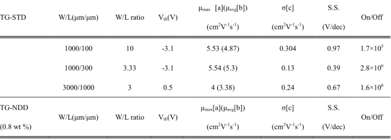
2.1 Comparisons of typical parameters in TG-STD and TG-NDD a-IGZO TFTs. ... 50
2.2 The intrinsic mobility of a-IGZO with 0.2 and 0.8 wt% nano dot doping... 54
2.3 Typical parameters of BG-NDD TFTs with and without nano-dot doping. ... 59
1
Chapter 1.
Introduction
1.1. Overviews of Metal-Oxide Semiconductor
Thin-film transistors (TFTs) based on metal-oxide semiconductors were considered a promising candidate for next generation semiconductors [1]. With a high
mobility (> 10 cm2/Vs) and a low subthreshold swing (0.2 V/decade) under low fabrication process, a-IGZO semiconductors have received considerable attention
because of the applications on liquid-crystal displays, electrophoretic displays, and organic light-emitting diode displays [2,3]. In addition, the large band gap of the
a-IGZO semiconductor (>3 eV) results in high transparency, insensitivity to natural light, and transparency in visible region (λ = 400-700 nm) [4,5]. Moreover, the carrier
concentration of a-IGZO film can be controlled by modulating oxygen ratio, process power, and pressure. Radio-frequency sputtering, which enables deposition of thin
films with high-melting-temperature materials over large areas at low substrate temperatures, is one of the methods used to deposit a-IGZO films [6].
Hosono et al. proposed that the chemical species and/or a structure in a thin film are unstable when thin films are deposited at low temperatures [6][7]. The chemical
species and/or a structure are frozen in the as-deposited thin film, which relaxes to a more stable state and provides the atoms with more energy to rearrange after thermal
annealing, leading to a desirable change in the electron transport properties [6][7]. Most oxide TFTs, especially a-IGZO TFTs, are fabricated by using physical vapor
deposition (PVD) techniques at room temperature and often require a high temperature (> 300 ℃) post-deposition thermal annealing process to obtain
2
1.1.1. Fundamental Transport Mechanism of Metal-Oxide Semiconductor
The a-Si:H material composed of covalent bonds of sp3orbital is shown in
Figure 1.1 [10]. The electronic levels and trap states were influenced by the
fluctuation of the bonding angle in the a-Si:H structure [11]. By contrast, conduction band minimums (CBM) of oxides are composed of spherically extended orbitals of
metals, and their overlaps with neighboring metal orbitals (s orbital) are not considerably altered by disordered amorphous structures; therefore, electronic levels
of CBM are insensitive to local strained bonds, and electron transport is not considerably affected (Figure 1.2). Therefore, a-IGZO exhibits high mobility, even in
an amorphous structure [10].
3
Figure 1.2 The carrier transport paths in amorphous oxide semiconductors.
Each element in a-IGZO film exhibits various characteristics that affect the
performance of TFTs. A high In concentration is expected to obtain high electron concentration [11] because the element of In is a large atom that easily loses electrons.
The released electron from In may move to the conduction band when the composition of a-IGZO lacks oxygen [12]. Ga was chosen because the atomic radius
of Ga is close to In. Hosono et al. reported that the Ga3+ in the a-IGZO film attracts oxygen tightly because of the high ionic potential resulting from the small ionic radius
and +3 valence. It suppresses the electron injection and induces the oxygen ions escaping from the a-IGZO film, providing relatively high stability for the device. [13].
Compared to the carrier concentration in the material of a-IZO (~1021 cm-3), a lower carrier concentration of a-IGZO (~1019 cm-3) was observed [13][14]. However,
incorporation of Ga decreases carrier density and mobility. The largest mobility of 39 cm2/Vs was obtained for Zn-doped In O (a-IZO). However, it is difficult to control
and maintain a low carrier density, which is necessary for efficient TFT operation for Ga-free or Ga-poor films. Therefore, the incorporation of Ga is crucial to obtain stable
films and TFTs. The element of Zn in the a-IGZO film was reported to affect the crystallization of thin film. The crystalline structure was reported when the ratio of the
Zn atoms in the a-IGZO film was higher than 65% [12]. The crystalline structure in a-IGZO film may degrade the electrical characteristic when uniformity is decreased
4
1.1.2. Oxygen Vacancy on a-IGZO Films
The oxygen vacancy formation process is closely related to the generation of charge carriers, according to (1).
O = O + V..+ 2e (Eq.1)
In (1), O is lost from the oxide sub-lattice (O ) to create a doubly charged oxygen vacancy (V..) and two free electrons. It is assumed that IGZO films attained more
charge carriers because of thermally enhanced or energy-activated oxygen vacancy formation processes. It was reported that the mobility of a-IGZO films depends on the
carrier concentration because the carrier transport is governed by percolation conduction over trap states and is enhanced at high carrier concentrations by filling
the trap states [10].
The chemical and oxygen binding energy of O were analyzed by X-ray
photoelectron spectroscopy (XPS) to understand the oxygen vacancy in a-IGZO films. This analytical method was used to investigate the origin of carriers in IGZO. By
Gaussian fitting, these O peaks were divided into three peaks, centered at approximately 530.5, 531.5, and 532.5 eV. The peak with the lower energy value of
530.5 eV represents O2- ions combined with Zn, Ga, and In ions in the IGZO compound system. This indicates the stoichiometric ratio between the metal cations
and oxygen anions. The medium binding energy value at 531.5 eV is associated with O2- ions that are in oxygen vacancy regions within the IGZO films. Therefore, the
change in the intensity of this peak may be connected to a variation in the concentration of oxygen vacancy. The higher binding energy value of 532.5 eV is
related to loosely bonded oxygen on the IGZO surface, including absorbed H2O, CO3,
and O2. The peak may be eliminated completely when the film is annealed or slightly
5
1.1.3. Argon Plasma Treatment on a-IGZO Films
The influence of Ar plasma treatment on a-IGZO thin films was investigated. The net electron carrier concentration (1020–1021 cm−3) of the a-IGZO thin films
considerably increased after exposure to the Ar plasma compared to that (1014 cm−3) of the as-deposited thin film. Furthermore, sheet resistivity considerably decreased
after Ar plasma treatment lasting several seconds. Energetic Ar ion bombardment during plasma treatment induces the preferential sputtering of the relatively light
atoms from the surfaces of II-VI or III-V group semiconductors because of the physical momentum transfer between the ions in the plasma and the atoms on the
material surface. Therefore, the substantial change in electron concentration after exposure to the Ar plasma may be caused by the oxygen deficiency on the a-IGZO
film surface [16].
1.2. Overviews of Organic Semiconducting Materials
In recent years, flexible display has been one of great interest especially in
mobile applications. However, flexible substrates cannot sustain under high temperature fabrication process, the development of low temperature process of
electronics is necessary. Organic semiconducting materials have high potential due to the following advantages: 1) low-cost; 2) solution fabrication process on a large area array system; 3) low fabrication temperature (< 200 ℃); and 4) the applications are
on a flexible substrate.
Recently, organic materials are extensively applied on electronic devices, such as light emitting diode(LED), thin film transistors(TFT), solar cells, and sensors. Also,
organic chemical products are closely related to our life, such as foods, medicines, paper, plastics, and fibers. There are two kinds of organic semiconducting materials
6 of organic materials as following.
1.2.1. Polymers
The conventional polymer is extensively used due to their plastic deformability, mechanical strength, low weight, and usually high resistivity. In 1970, the Japanese
chemist Shirakawa found that it was possible to synthesize polyacetylene (CH)n in a
new way. Shirakawa synthesized trans-polyacetylene by accidentally adding “a
thousand-fold too much catalyst” to the reaction vessel. Shirakawa was stimulated by this discovery. The corresponding reaction at another temperature gave a
copper-colored film instead, and it appeared to consist of almost pure
cis-polyacetylene. Around the same time chemist Alan G. MacDiarmid andphysicist
Alan J. Heeger were experimenting with a metallic-looking film of the inorganic polymer sulphur nitride, (SN)x. When MacDiarmid heard about Shirakawa'sdiscovery
at a seminar in Tokyo, he invited Shirakawa to the University of Pennsylvania in Philadelphia. After Shirakawa and MacDiarmid modifiedpolyacetylene by oxidation
with iodine vapor, they knew that the optical properties changed in the oxidation process and asked Heeger to have a look at the films. Aftermeasured the conductivity
of the iodine-doped trans-polyacetylene, the incredibleincrease of ten million times the original conductivity was discovered. In the summerof 1977, Alan Heeger, Alan
MacDiarmid and Hideki Shirakawa, and co-workers,published their discovery in the article "Syndissertation of electrically conducting organic polymers: Halogen
derivatives of polyacetylene (CH)n" in The Journal of Chemical Society, Chemical
Communications.[17] The discovery was considered a majorbreakthrough, and Alan
Heeger et al. have beenawarded the Nobel Prize in Chemistry in the year 2000 for showing how plastic canbe made to conduct electric current.[18] Since the field has
7
properties of a polymer are strongly related to the physical arrangement ofmonomers
along the backbone of the chain. Polymers which contain only one type ofmonomer are known as homopolymers, while polymers containing a mixture ofmonomers are
known as copolymers.
The conducting conjugated polymer consists of a long chain of carbon atoms with
alternating single and double bonds between them, each with one hydrogen atom. The structure of polyacetylene is shown in Figure 1.3(a) as a typical example.
Polyacetylene is usually prepared in the cis- form which can be converted into the thermodynamically more stable tans- form by thermal isomerization. Other
semiconducting conjugated polymers shown in Figure 1.3 are commonly used in organic light-emitting diodes (OLEDs), organic field-effect transistors (FETs), and
organic solar cells. As shown in Figure 1.3(b), PEDOT:PSS is a water-soluble transparent conducting polymer, which enabled the fabrication of all plastic polymer
light-emitting diodes (PLEDs). PEDOT:PSS can be used as a transparent anode. Currently, it serves as the hole transport layer to develop PLEDs for commercial
products. Structures of PPV and PPV derivatives (MEH-PPV) are shown in Figure
1.3(f) and 1.3(h). The most commonly used PPV is typically deposited by spin
coating a precursor polymer, and then thermal treatment is used to convert the precursor to PPV. PPV also used as hosts for low gap emitter.[19] PFO is also the
material used in the blue PLEDs as shown in Figure 1.3(g). Following the first blue PFO-based PLED was developed in 1991 [20], efforts was conducted on developing
commercially viable devices based on these polymer. Polythiophenes and P3HT-based PLEDs and FETs are widely studied.[21], [22] Due to it relatively low
gap, the polythiophenes are red emitters. However, the relatively poor lifetime of polythiophene-based PLEDs inhibits their commercialization. On the other hand,
8
be increased and the performance of the FETs can be optimized.
Figure 1.3 Molecular structure of widely used conjugated polymers: (a) polyacetylene;(b) poly(3,4-ethylenedioxythiophene) : poly(styrenesulfonate) (PEDOT:PSS); (c)poly(9,9-dioctylfluorene-co-N-(4-butylphenyl)diphenylamine) (TFB);(d)poly(9,9-dioctylfluorene-co-bis-N,N-(4-butylphenyl)-bis-N,N-phenyl-1,4-p
henylenediamine) (PFB); (e)
poly[N,N'-bis(4-butylphenyl)-N,N'-bis(phenyl)-benzidine] (polyTPD); (f)poly(p-phenylenevinylenes) (PPV); (g) poly[9,9-dioctylfl uorenyl-2,7-diyl] (PFO); (h)poly-[2-methoxy,(5-2'-ethyl-hexyloxy)-p-phenylenevinylene] (MEH-PPV); (i)poly(9,9-dioctylfluorene-co-benzothiadiazole) (F8BT); (j) poly[3-hexylthiophene](P3HT); (k) poly[5,5'-bis(3-alkyl-2-thienyl)-2,2'-bithiophene) (PQT); (l)poly[(9,9-dioctylfluorene-co-bithiophene] (F8T2); (m)
9 poly(9-vinylcarbazole) (PVK).
1.2.2. Small molecular weight materials
The phenomenon of organic electroluminescence was first discovered by Pope in 1963.[23] However, the development of organic light-emitting diode actually began in
the late 1970s by Tang and his coworkers. Their research led eventually to the discovery of the first efficient multi-layered organic electroluminescent device.[24]
Since then, tremendous progress has been made in the field of organic electroluminescence. Among all efforts to improve the performance of organic
light-emitting diode, the continuing discovery of new and improved electroluminescent materials is the most essential one. Small molecular weight
materials consist of molecules with several to a few hundred atoms. Small molecular weight materials were the initial focus of physicists and engineers who seeking to
understand the optoelectronics properties of organic materials. Structure of some small molecular weight materials are shown in Figure 1.4. Figure 1.4(a) shows the
structure of CuPC which is widely used as an hole transport layer. However, depending on the other layer, it may inhibit hole injection [25] or enhance it [26].
TPD is another material commonly used as hole transport layer as shown in Figure
1.4(b). But, its relatively low glass transition temperature around 65℃ causes a
failure of OLED as TPD recrystallized. The recrystallization may be suppressed by adding guest molecule such as rubrene. However, it may result in red
electroluminescence from rubrene. Hence, NPB is developed with a structure similar to TPD but the methylphenyl groups are replaced by naphthylphenyls. The
modification significantly enhances the stability of the OLED due to the increased glass transition temperature around 95℃.
10
OLEDs. It is still one of the most robust electron-transport backing layers in OLED,
particularly with the help of the hole blocking layer to trap the hole carriers from injecting into Alq3.[27] It is not only commonly used as a green emitter, but also as a
host for lower-gap emitter guest molecules. It has been found by the time-of-flight technique that the drift mobility of electrons in Alq3 is increased by about two orders
of magnitude (to 10-4 cm2/Vs) as the deposition rate decreased from 0.7 to 0.2 nm/s.
Figure 1.4 Molecular structure of widely used small molecular weight materials: (a)
copper phthalocyanine (CuPC); (b)
N,N'-Bis(3-methylphenyl)-N,N'-bis-(phenyl)-benzidine (TPD); (c) N,N-bis(1-naphtalenyl)-N-N’-bis(phenylbenzidine) (α-NPB);
11
(d)N,N’-bis(2-naphtalenyl)-N-N’-bis(phenylbenzidine) ( β -NPB); (e) 4,4',4" -Tris(N-(1-naphthyl)-N-phenyl-amino)triphenylamine (1T-NATA); (f) 4,4',4" -Tris(N-(2-naphthyl)-N-phenyl-amino)triphenylamine (2T-NATA); (g) α-sexthiophene (α-6T);(h) Pentacene; (i) Tris(8-hydroxyquinoline) Aluminum (Alq3T); (j) (5,6,11,12)-Tetraphenylnaphthacene (Rubrene); (k) 2-(4-Biphenylyl)-5-
(4-tert-butylphenyl)-1,3,4-oxadiazole (PBD); (l)
4-(Dicyanomethylene)-2-tert-butyl-6-(1,1,7,7-tetramethyljulolidin-4-yl-vinyl)-4H-pyr an (DCJTB).
1.3. Overviews of Organic Sensors
1.3.1. Organic Photodetector
Organic electronics have attracted considerable interest because of their low
fabrication temperature on a variety of low-cost flexible substrates, which enables the development of organic photonic integrated circuits, organic sensor arrays, organic
photocouplers, or organic imaging sheets. The two main organic photodetectors used currently are as follows: (1) organic photodiode (OPD) and (2) organic phototransistor
(OPT). The mechanism and the characteristics of these two photodetectors are discussed in the following paragraphs.
1.3.1.1. Organic photodiode
According to the research of organic photodiodes and solar cells, the light is mainly
adsorbed by the organic materials and generates the high binding energy of excitons. The high binding energy of excitons causes difficulty in dissociating the electrons and
holes. In Figure 1.5, the photodetector is through the dissociation of photogenerated excitons at the interface between donor-like materials and an acceptor-like material
under reversed bias. The performance of an OPD is determined by the efficiency of charge generation and charge transport.
12
Figure 1.5 The operation mechanism of photo diode.
The quantum efficiency of an OPD can be enhanced by creating a bulk-heterojunction,
and the charge transport property can be improved by using high mobility materials. Increasing the interfaces of the hole transporting layer and electron transporting layer
with a blending system (for example, P3HT:PCBM) was proposed to enhance the external quantum efficiency (EQE). However, the blending system may decrease the
frequency response of photodiodes because of the increasing recombination rate. The bilayered system may be used to decrease the recombination rate of electrons and
holes to increase frequency response. Forrest et al. (2000) proposed the highest operation frequency (~430 MHz) of organic multilayer OPDs by using
ultrahigh-vacuum (1×10⁻¹⁰torr) organic molecular beam deposition to control the thickness of an individual layer as 0.5 nm, to enable carrier tunneling [28]. The device
structure and the J-V curve are shown in Figure 1.6(a), and the photoresponse is shown in Figure 1.6(b).
13
Figure 1.6 (a) The current density as a function of voltage (J-V), inset of Figure 1.7(a)
is the device structure. (b) The frequency response of device.
When a conventional high vacuum (5×10⁻⁷ to 1×10⁻⁶ Torr) deposition system was used, a multilayered PD was reported to exhibit a bandwidth from a few kilohertz to a few
megahertz under an operation voltage of 1–5 V, and demonstrated a small incident photon to current conversion efficiency IPCE of 0.02% [29]. Morimune et al. used a
bilayered structure to demonstrate a bandwidth of 70 MHz under 7 V operation, with the peak IPCE at approximately 7% [30]. High frequency responses were
demonstrated in these studies; however, factors associated with organic materials to influence frequency response were not discussed. In Chapter 3, we propose an
adjustment of the vertical mobility to influence the frequency response and obtain an ultrahigh response of 80 MHz.
1.3.1.2. Organic phototransistor
Compared to OPD, the OPT exhibits a higher photoresponsivity because of the threshold voltage shift after exposure to light, and it may be used on flexible
substrates and integrated with a circuit.
In organic semiconducting materials of phototransistors, pentacene is one of the most
14
field-effect mobility and the threshold voltage varied, and the pentacene-based
phototransistor was exposed to light [31]. This occurred because the photo penetrated to the interface between the active layer and dielectric, and generated the extra
electron and hole pairs to contribute the photo current. In addition, after exposing to light for a specific period, the generated electron may induce negative traps and cause
a threshold voltage shift. In previous research [32], threshold voltage largely shifted when the device was exposed to light with positive gate voltage, and led to the
increased photoresponsivity of the device. The increased photoresponsivity occurred because the generated electron by exaction may attract through the positive voltage,
and the electron was limited in the channel to form the traps. By contrast, the generated hole by excitons may extract from the channel and decrease the
recombination rate. In addition, it was proposed that the electron trap induced by a photo has a lengthy life time; however, it may recover quickly by applying the
positive voltage [33]. OPTs have high photoresponsivity; however, the frequency response is considerably slow because the reaction includes the trap generation, that is,
the capture and release of carriers.
1.3.2. Ammonia Sensors
1.3.2.1. Applications of Ammonia Sensors
Ammonia is a crucial compound. It can be used in several fields, such as chemical industries, fertilizer factories, refrigeration systems, food processing, fire power plants,
and medical diagnoses. The variation in ammonia concentration is crucial for these applications. For example, in chemical industries, ammonia concentration is related to
the quality of fertilizers and frozen foods. Additionally, ammonia concentration plays a vital role in medical diagnoses. Table 1 shows the component of human breath
15
ammonia is a disease marker for uremia, liver cirrhosis, and renal failure
[34][35][36][37].
Table 1.1 Diseases associated with unusual breath odors.
Breath component as a
disease marker
Diseases References
Acetone Diabetes; Lung cancer [34], [35]
Ammonia Uremia; Chronic liver disease [36], [37]
Butyric acid Liver cirrhosis [37]
Ethanethiol Liver cirrhosis [37]
Hydrogen sulfide Periodontal disease [37]
Table 2 shows the gas concentration with various healthy conditions [36][38]
[39]. The breath ammonia concentration of patients is 1-5 ppm for renal failure, and 0.5-1 ppm for liver cirrhosis.
The common method used for diagnosis is an examination of the ammonia concentration in blood. Recently, developments of a noninvasive diagnostic method
have received considerable attention. The breath of patients can be detected easily and traced by the gas sensor if a noninvasive, inexpensive, portable, and disposable
16
Table 1.2 The gas concentration with different healthy conditions
Renal failure Liver cirrhosis Diabetes References
Ammonia 4.8 ppm 0.5-1 ppm [36], [38]
Acetone 5-300 ppm [39]
1.3.2.2. Different Types of Ammonia Sensors
(a) Metal-oxide gas sensors
ZnO[40], iridium oxide [41], molybdenum oxide [42], polyaniline [43][44][45], polypyrrole [46], Au and MoO3-modified WO3 [47][48], and Pt- and SiO2-doped
SnO2 [49] are commonly used materials for ammonia gas sensing. When the device is exposed to analytes, the gas removes some of the adsorbed oxygen and modulates the
height of the potential barriers, thereby changing the conductivity and creating the sensor signal. However, ammonia sensors based on metal oxide must be operated at high temperature (over 300 ℃), and are not useful as noninvasive ammonia sensors.
(b) Catalytic ammonia sensors
The reaction of a catalytic ammonia sensor is based on a metal layer with ammonia
gas. The reaction causes a change in electrode potential and charge carrier concentration, which can be quantified by using a field-effect device, such as a
capacitor or a transistor [50][51].
(c) Conducting polymer gas detectors
Conducting polymer ammonia gas detectors used polymers, such as polypyrrole or
polyaniline, to react with ammonia. During this process, ammonia can reversibly reduce the oxidized form of polymer. Because the reduction in the polymer film
17
causes a change in the conductivity of material, it can be used for resistometric or
amperometric ammonia detection [52]. However, the irreversible reaction between ammonia and the polymer causes the sensitivity of the sensor to decrease when
exposed to ammonia.
(d) Optical gas analyzers
Two optical methods are used for the detection of ammonia. The first method is the
Berthelot reaction, which uses a coloration reaction of ammonia with phenol and hypochlorite in aqueous solutions [53][54]. The disadvantage of this method is the
slow kinetics of the reaction. The detection limit is approximately 5 μM of ammonia in water or 90 ppb. The second method is optical absorption ammonia detection [55].
A spectrum of the light influenced by the gas composition can be obtained by using a laser and a spectrograph. Although the method is sensitive and selective for ammonia
sensing, the equipment is expensive and is unsuitable for miniaturized ammonia sensors.
1.3.2.3. OTFTs Ammonia Gas Sensors
Research on OTFT sensors began in the late 1980s, after the first OTFTs were proposed. Such sensors offer the advantages of simple process, low fabrication cost,
remarkable response repeatability [56], and selectivity [57][58]. Because several types of organic molecules exhibit sensing behavior based on their chemical compositions,
sensibility and selectivity can be pursued by choosing chemically or biologically functionalized semiconducting polymer active layers for the use of OTFTs in compact
sensing systems or in biochips [56][59][60][61]. In addition, [59] and [62] verified that the OFET sensor exhibited superior performance than a similar resistor-type
18
operating temperature. In particular, OTFTs were proposed as multi-parameter sensors
[63]. A fingerprint of each gas can be obtained by measuring the parameters of field-induced conductivity, threshold voltage, and field-effect mobility. This enables
the transistors to be more selective than conventional chemiresistors. The morphology of the active layer plays a crucial role in the sensibility of OTFT sensors. The device
response increases when the grain size is reduced [64]. The effect of a channel length compared to the grain size was also observed. Nanoscale organic transistors were
explored to improve the limit of detection [65].
The active layer of OTFT sensors currently include substituted thiophene
polymers, oligomers, naphthalenes, copper-phthalocyanine, and pentacene. These devices were exposed to various analytes, such as alcohols, ketones, thiols, nitriles,
and ester and ring compounds. However, research on ammonia sensors with OTFTs is limited. Our study is the first to demonstrate the pentacene-based OTFTs as ammonia
gas sensors.
Finally, Table 3 shows a comparison of the ammonia sensors proposed in this study
and those of other studies [66][67][68][69][70][71][72]. Currently, only optical sensing systems exhibit a sensitivity in parts-per-billion (ppb) or even
parts-per-trillion (ppt) regime. Electrical ammonia sensors, such as poly(3-hexylthiophene)(P3HT)-based OTFT, exhibit sensitivity higher than 10 ppm.
Electrical sensors based on catalytic metals exhibit sensitivity of 1 ppm; however, the sensors must be operated at a temperature higher than 150 ℃. Our proposed
pentacene-based OTFT, particularly the UV-treated pentacene-based OTFT, exhibited sensitivity of 0.5 ppm at room temperature.
19
Table 1.3 This table compares the ammonia sensors of this work and of others reports
Principle Low detection limit Response time Temperature range Remarks[ref.] Optical gas sensors
/Nessler
90 ppb ~1 min 37℃ To detect in water[66] Optical gas sensors
/Coulorometric
1 ppt ~5 min N/A Expensive setup[67] Optical gas sensors
/Absorption spectroscopy
1 ppb ~5 min N/A Expensive setup[68] Catalytic metal
/ Palladium
1 ppm ~1 min Up to 600℃ Low selectivity[69] Catalytic metal
/ Polyaniline
1 ppm ~1 min Up to 150℃
Irreversible reactions [70], [71]
OTFT/P3HT 10 ppm 2~3 min RT Low sensitivity[72]
Our proposed
/ pentacene-based OTFT
0.5 ppm ~ 500 sec RT
Low cost and high sensitivity
1.4. Overviews of Organic Transistors
1.4.1. Organic Field-Effect Transistors
The beginning of the electronics was marked by cathode ray tube, vacuum
rectifier, and vacuum-tube triode. The triode, includes a grid between the anode and the cathode, transformed communication and long-distance telephone come true.
However, the vacuum-tube d the rectifier into an amplifier, and made the radio triode was fragile, slow, and difficult to miniaturize.
Replacing the triode with a solid-state device offering an alternative to the thermionic principle is thus a good idea for solving problems of triode. This concept was
successfully demonstrated with Bardeen and Brattain’s point-contact transistor and Shockley’s bipolar transistor. After material technology research for more than forty
20
years, the performance of metal-oxide-semiconductor field-effect transistor
(MOSFET) is optimized. Today, MOSFETs dominated almost every electronic device. Recently, organic field-effect transistors (OFETs) based on solution-processed
polymeric as well as small molecular semiconductors have obtained impressive improvements in their performance. Even an all polymer transistor has been reported.
[73] Initially, the interest in organic transistors remained limited due to the poor performance of these initial devices. Several review papers and books describing the
materials, operating principles, and fabrication processes have been published for comprehensive understanding. ([74], [75])
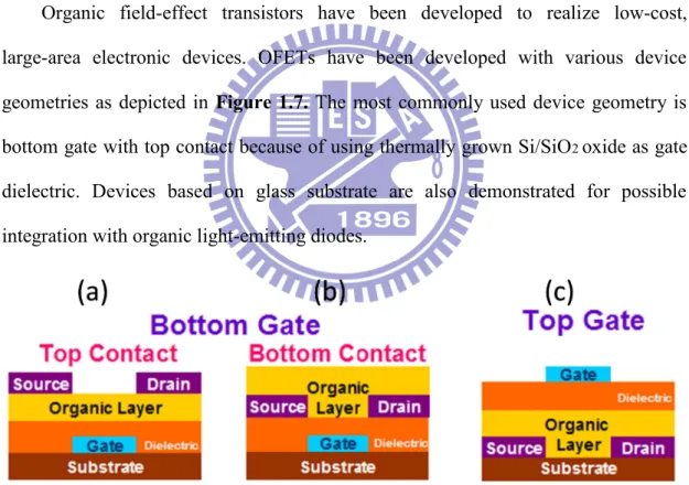
Organic field-effect transistors have been developed to realize low-cost, large-area electronic devices. OFETs have been developed with various device
geometries as depicted in Figure 1.7. The most commonly used device geometry is bottom gate with top contact because of using thermally grown Si/SiO2 oxide as gate
dielectric. Devices based on glass substrate are also demonstrated for possible integration with organic light-emitting diodes.
Figure 1.7 Schematic of the bottom-gate organic field-effect transistors with (a) top
contact or (b) bottom contact structures. (c) Schematic diagram of a (c) top-gate with bottom contact transistor using a standard TFT device structures.
Carrier mobilities in organic semiconductors are limited by the hopping process between the molecules in disordered regions of the material. Many research works
21
molecular weight [77], and side-chain length [78]) and processing conditions (film
thickness [79], doping level [80], thermal annealing [81], and the film-forming method [82]). Studies of semiconductor/insulator interface phenomena (such as
surface-mediated molecular ordering, surface dipoles, semiconductor alignment using self-assembled monolayers (SAMs), physical treatment, and photoalignment) are also
receiving attention for enhancing the electrical properties of organic semiconductors. SAMs are highly ordered, two-dimensional structures that form spontaneously on a
variety of surfaces. Tuning of the interfacial surface can be achieved by varying the rigidity, length, and terminal functional group of the molecule, which in turn affects
the uniformity, packing, conformation, polarity, and charge density of the surface. Fluorene copolymers and polythiophenes have a relatively rigid backbone with
attached alkyl chains for solubility, and are able to crystallize. Charge transport is fastest in the conjugation direction as shown in Figure 1.8(a).[83] When chains pack,
the π-orbitals belonging to different polymer chains are stacked co-facially, and this partial overlap between π-orbitals assists inter chain charge transfer. However, in
another direction, the insulating alkyl chains impede charge transport so that mobility in this direction is the lowest. Such anisotropy has been experimentally verified by
comparing the electrical characteristics of TFTs and diodes. Because of this pronounced anisotropy, texture and relative orientation of crystallites are expected to
22
Figure 1.8 Molecular and crystallographic structures (orthorhombic unit cell) of
P3HT chains show the enhanced π–π overlap along the b direction. [83]
1.4.2. Organic Vertical Transistors
An explosion of interests in flexible electronics made from organic semiconductors gave rise to extensive research on organic light-emitting diodes
(OLED), organic field-effect transistors (OFET), organic chemical sensors, and organic solar cells. One of the key components of the flexible electronics is the
organic FET, a horizontal device with source and drain electrodes on the same plane. Its operating voltage usually over 25 V due to low carrier mobility and long channel
length. The characteristics of organic FETs can be strengthened by increasing the mobility [83], utilizing a self-assemble monolayer as gate dielectrics [85] and
reducing the channel lengths to the submicron [86]. Horizontal organic FETs with submicron channel lengths made by electron-beam lithography [87], nanoimprint
lithography [88] and soft contact lamination [89] have been demonstrated. Vertical organic FETs, whose channel length was determined by the thickness of an insulating
layer between source and drain, have been made by solid-state embossing [90], excimer laser [91] and photolithography [92]. However, the inherently low mobility
23
organic materials create great limitation on the device performance and the fabrication
process for organic FET. The unique advantages of organic materials such as low-cost and large-area solution process are so far not fully explored for high-performance
FET. Vertical non-field-effect transistors with multilayer structures give another route to circumvent the limits of both horizontal and vertical field-effect transistors. In
vertical non-field-effect transistors, the channel length can be easily defined by the total thickness of the organic layers, and the current is modulated by a conductive
layer embedded in the organic materials. Various device operating principles were proposed with different types of conductive layers such as a thin metal film[93], a
strip-type metal film[94], a mesh gate electrode[95], and a porous conducting polymer network[96]. The remaining problems are the low current density, low on/off ratio as
well as the complex fabrication process. One promising direction is to turn a vacuum tube triode into a solid-state device with current limited by the space-charge-limited
current. Here, the vertical transistor is called “space-charge-limited transistor.” The operation mechanism of the SCLT can be understood as the quadratic space charge
limited current between the emitter and the opening modulated by the grid potential. As in vacuum tube, the potential at the center of the opening is a linear combination
of grid and collector potential kVG + VC, the factor k depends on the device geometry and increases with the ratio between the opening diameter and the grid-collector
distance. The SCLC between the emitter and the opening is therefore approximately
C
VG VC
2/ L3, where ɛ is the polymer dielectric constant and L is theemitter-grid distance. If the potential across the opening were uniform, the factor C
would be the standard SCLC value of 9/8. The overall effect of non-uniform potential in our case can be absorbed into a numerical factor C. Because of the higher electric
24
therefore the emitter-opening current given above is actually the output current.
Table 1.4 shows the different types of vertical transistors and classified three
types: (1) vertical organic field-effect transistor, VOFET (Y Yang et al.)[97], (2) hot
carrier transistor, HCT (H. F. Meng et al.) [98] and metal-base transistor, MBT (I. A. Hümmelge) [99] (3) space-charge limited transistor, SCLT (H. F. Meng et al.) [100]
and static induced transistor, SIT (Kudo et al.) [101]. Most of the devices are operated at low voltage (<5 V) with high output current density ( >10 mA/cm2). For the first
type transistor (VOFET), the transistor can obtain high on/off current ratio due to the transistor is operated at normally-off mode. However, it is difficult to develop for
large area because it needs to deposit thin charge injection layer (2.5 nm) between source electrode and organic layer for improving the gate controllability. Also, the
uniformity of the thin charge injection layer is difficult to control. The operation mechanism of second type transistor (HCT or MBT) is similar to BJT, the output
current have saturation region. However, the carriers have to tunnel from base metal to collector, therefore, the film thickness of base metal have to be well controlled. For
the third type transistor (SCLT or SIT), it does not need to deposit ultra-thin base metal due to the porous base structure. However, the low on/off current ratio and high
leakage current are needed to solve. In the chapter 6, we proposed a new structure of vertical transistor and successfully solved these two issues.
25
Table 1.4 Comparison of different types vertical transistors.
Reference
[1] M. Orita, H. Ohta, M.Hirano, S. Narushima, H. Hosono, “Amorphous transparent conductive oxide InGaO3 (ZnO)m (m les 4): a Zn 4s conductor” Philosophical
magazine B, 81, 501,(2001).
[2] H. Yabuta, M. Sano, K. Abe, T. Aiba, T. Den, H. Kumomi, K. Nomura, T.
Kamiya, H. Hosono, “High-mobility thin-film transistor with amorphous InGaZnO channel fabricated by room temperature rf-magnetron sputtering” Appl.
Phys. Lett. 89 ,112123, (2006).
[3] A. Tsukazaki, A. Ohtomo, T. Onuma, M. Ohtani, T. Makino, M. Sumiya, K.
Ohtani, S. F. Chichibu, S. Fuke, Y. Segawa, “Repeated temperature modulation epitaxy for p-type doping and light-emitting diode based on ZnO” Nature