國
立
交
通
大
學
電機與控制工程系
碩
士
論
文
利用雜訊功率模型、非線性失真模型
與功率消耗模型,以最佳化離散時間
單迴路積分三角類比數位轉換器
Design Optimization of Discrete-Time Single-Loop
Sigma-Delta ADCs based on Analytical Models of Noises,
Nonlinear Distortions, and Power Consumptions
研 究 生:李孟學
指導教授:陳福川 教授
利用雜訊功率模型、非線性失真模型與功率消耗模
型,以最佳化離散時間單迴路積分三角類比數位轉
換器
Design Optimization of Discrete-Time Single-Loop
Sigma-Delta ADCs based on Analytical Models of Noises,
Nonlinear Distortions, and Power Consumptions
研 究 生:李孟學 Student:Meng-Syue Li
指導教授:陳福川 Advisor:Fu-Chuang Chen
國 立 交 通 大 學
電 機 與 控 制 工 程 系
碩 士 論 文
A ThesisSubmitted to Department of Electrical and Control Engineering
College of Electrical Engineering and Computer Science
National Chiao Tung University
in partial Fulfillment of the Requirements
for the Degree of
Master
in
Electrical and Control Engineering
August 2007
Hsinchu, Taiwan, Republic of China
利用雜訊功率模型、非線性失真模型與功率消耗
模型,以最佳化離散時間單迴路積分三角類比數
位轉換器
研究生:李孟學 指導教授:陳福川 教授 國立交通大學 電機與控制工程研究所摘要
傳統的積分三角類比數位轉換器電路規格設計是一個相當耗時的工作,且需要不斷的 嘗試各種電路規格,以達到所需要的解析度。本篇論文分析了積分三角類比數位轉換器 的主要雜訊來源與非線性特性所造成的失真問題。藉由分析推導出的失真功率模型、雜 訊功率模型及絕對功率消耗模型,並以訊號對雜訊和失真比(SNDR)來當作我們的設計 規格,以做最佳化的設計。此最佳化設計意指在特定系統規格下(如頻寬、訊號對雜訊 和失真比),找到一組最佳化的設計參數,使得類比數位轉換器的功率消耗最小以及訊 號對雜訊和失真比最大,並節省龐大制定電路規格的時間成本。最後我們將針對已發表 的設計結果來做驗證的工作。雖然現今已存在相當多行為模擬工具以自動化制定電路規 格,但較之下,本論文所提出的最佳化方法將快上許多。Design Optimization of Discrete-Time Single-Loop
Sigma-Delta ADCs based on Analytical Models of
Noises, Nonlinear Distortions, and Power
Consumptions
Student:Meng-Syue Li Advisor:Dr. Fu-Chuang Chen
Institute of Electrical and Control Engineering Nation Chiao Tung University
ABSTRACT
The conventional sigma-delta ADC design approach is a time consuming process and needs much trials and errors. This paper analyze the mainly noise sources and nonlinear distortions. Utilizing the noise power models, nonlinear distortion power models and accurate power consumption models derived in this paper, and the assigned signal to noise and distortion ratio (SNDR) to be the design goal, we can forward to do design optimization under the specific specifications. Design optimization means that under the specific specifications (signal bandwidth, SNDR), we find a set of optimal design parameters such that the power consumption of ADCs is minimum and SNDR is maximum, and reduce the huge time-cost to set up the circuit specifications. Finally, design optimization is tested against a published design result. Although design automation issues have been partially addressed by recent behavior- simulation–based methods, yet such methods can be slower than our analytical approach far.
誌謝 Acknowledgment
我要將此論文獻給 我親愛的母親-廖甚 女士 最疼我的父親-李其昌 先生 我今生的摯愛-潘昭佑 小姐 若沒有他們,我不可能有機會完成此篇論文,並且從交通大學碩士班畢業。此外, 必須感謝指導教授陳福川博士兩年來嚴格的督促與指導,讓我學會做研究的方法與心 態。另外,也要感謝口試委員林清安教授、蘇朝琴教授與董蘭榮博士對本篇論文所給予 的建議與指導。 還要感謝實驗室英瑋學長在我一年級時幫我打好深厚的研究基礎。感謝實驗室同學哲 安、基恩和學弟文佑、俊傑、柏年陪我度過最後的學生生涯,並在研究上給予我很多幫 助。感謝研二舍710 室室友淳正、淳泰與士榮,謝謝你們在這兩年間帶給我的鼓勵和歡 樂,我以後會很懷念晚上刁牌的日子。感謝軍中黃文顯排長對我的鼓勵,我才能進入交 通大學就讀,且順利完成這兩年學業。 最後要謝謝這兩年在新竹唸書期間所有幫助過我的人,雖然無法一一列舉,但在這 邊向大家致上最大的謝意。Contents
中文摘要 ... I English Abstract ... II Acknowledgment... III Contents ...IV Lists of Tables ...VII Lists of Figures ...IX List of Symbols ...XIII
Chapter 1 Introduction ... ..1
1.1 Current Status and Background ... 1
1.2 Motivation and Aims ... 1
1.3 Organization ... 3
Chapter 2 Fundamental Theorems of Sigma-Delta Modulators ... 5
2.1 Nyquist Sampling Theorm ... 5
2.2 Quantization Noise and Peak SNR ... 7
2.3 Techniques of Sigma-Delta Modulator ... 9
2.3.1 Oversampling Technique ... 9
2.3.2 Noise shaping ... 11
Chapter 3 Architectures of Sigma-Delta Modulator ... 13
3.1 First-Order Sigma-Delta Modulator ... 14
3.2 Single-Loop Second-Order Sigma-Delta Modulator ... 16
3.3 Single-Loop High Order Sigma-Delta Modulator ...17
3.4 InterpolativeSigma-Delta Modulator ... 18
3.5 MASH Architecture ... 19
3.7 Multi-bit Sigma-Delta Modulator use DEM Technique ... 22
3.7.1 Randomization Technique ... 23
3.7.2 Data Weighted Averaging (DWA) ... 23
3.8 Decimator ... 25
3.9 Performance Metrics for a ΣΔ Modulator ... 26
Chapter 4 Models of Sigma-Delta Modulator Noises and Power ... 27
4.1 Finite OTA Gain Error ... 29
4.2 Thermal noise (Switch, OTA, Reference circuits) ... 29
4.3 Settling Problem ………... 32
4.4 Multi-bit DAC noise ... 39
4.5 Clock Jitter Effects ...40
Chapter 5 Models of Sigma-Delta Modulator Nonlinear Distortion ...42
5.1 Settling Distortion ...42
5.2 Nonlinear Finite OTA Gain Distortion...50
5.3 Multi-bit DAC Distortion ...62
5.4 Quantizer Nonlinearity Distortion ………...71
5.5 Nonlinear Capacitance Distortion ...72
5.6 Nonlinear Switch Resistance distortion ...73
Chapter 6 Models of Sigma-Delta Modulator Power Consumption...76
6.1 Analog Power Consumption ...76
6.2 Digital Power Consumption ...78
Chapter 7 Design Optimization of Sigma-Delta ADCs Design ...81
7.1Design Parameters Discussions ...81
7.2 Design Optimization ...84
Chapter 8 Simulation Results ...86
Lists of Tables
Table 4.1 Standard deviations of
V
S vs. different quantizer bit numbers... 34 Table 5.1 Minimum SR and GBW required w. r. t. OSR
... 50 Table 5.2 The relationship between the each parameter and power of the harmonic
distortions
... 59 Table 5.3 Comparison of theoretic result and behavior simulation for case A
... 61 Table 5.4 Comparison of theoretic result and behavior simulation for case B
... 62 Table 5.5 Simulation results of standard deviation of capacitor mismatch vs. unit DAC
number with Ain=1
... 69 Table 5.6 Theoretical results of standard deviation of capacitor mismatch vs. unit DAC
number with Ain=0.5
... 69 Table 5.7 Simulation results corresponding to Table 5.6
... 70 Table 6.1. kOTA for three common OTA structures.
Table 7.1 Summary of noise and distortion-power and power-rating when design parameters increase
... 83 Table 8.1 Comparisons of our design results and those in [Gag 03] with different K
... 87 Table 8.2 the corresponding noise and distortion powers for the design parameters listed in
Table 8.1
... 98 Table 7.3 Listing the details of power consumption.
Lists of Figures
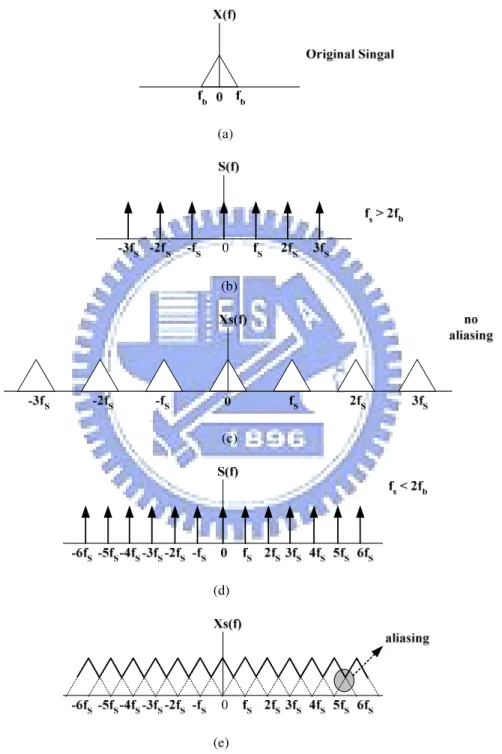
Fig. 2.1(a)Original signal spectrum (b)Sample function when fs > 2fB
(c)Signal spectrum that is sampled by (b) (d)Sample function when fs < 2fB
(e)Signal spectrum that is sampled by (d)... 6
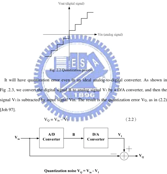
Fig. 2.2 Quantization process ... 7
Fig. 2.3 Quantization error caused by A/D converter ... 7
Fig. 2.4 Quantization error range ... 8
Fig. 2.5 P.D.F of quantization error ... 8
Fig. 2.6 Sampling system ... 10
Fig. 2.7 Noise distribution after sampling ... 10
Fig. 2.8 (a)General ΣΔ modulator (b)Linear model with quantization noise ... 11
Fig. 2.9 Noise shaping ... 12
Fig. 3.1 Block diagram of ΣΔ A/D converter. ... 13
Fig. 3.2 First-order ΣΔ modulator ... 14
Fig. 3.3 Single-loop second order ΣΔ modulator ... 16
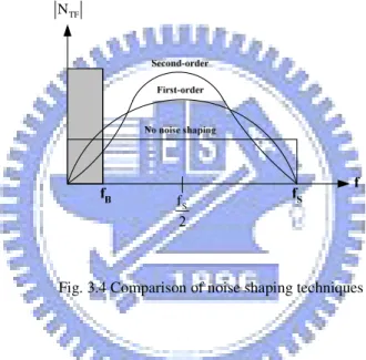
Fig. 3.4 Comparison of noise shaping techniques ... 17
Fig. 3.5 Single-loop high order ΣΔ modulator ... 18
Fig. 3.6 Four-order interpolative architecture ... 18
Fig. 3.7 2-1 architecture MASH ΣΔ modulator ... 19
Fig. 3.8 SNR vs. OSR with different quantizer bit number ... 21
Fig. 3.9 Multi-bit architecture ... 22
Fig. 3.11 Operation principle of the DWA algorithm ... 24
Fig. 3.12Output spectrum with three kinds of DAC ... 24
Fig. 3.13 Comparison of ΣΔ modulator architectures ... 25
Fig. 3.14Performance characteristic of a ΣΔ converter ... 27
Fig. 4.1 Integrator and the DAC branches... 28
Fig. 4.2 Equivalent circuits of sampling and integration phases... 31
Fig. 4.3A bandgap voltage reference circuit………... 32
Fig. 4.4Equivalent circuit while considering reference voltage noise………... 32
Fig. 4.5 Switched capacitor integrator diagram (a) Sampling phase (b) Integration phase …………..………...33
Fig. 4.6Simulated results of VS distribution ... 34
Fig. 4.7 Three types of settling conditions in integration phase... 36
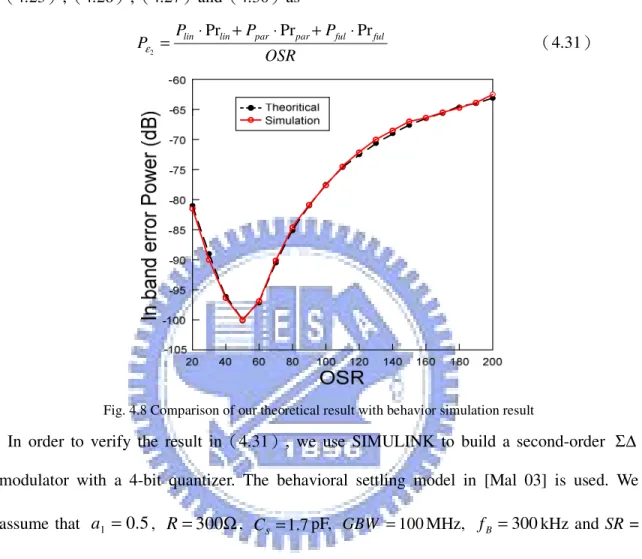
Fig. 4.8 Comparison of our theoretical result with behavior simulation result ………….…..38
Fig. 4.9 Main nonidealities sources in the ΣΔ modulator ………..………….…..41
Fig. 5.1 3D plot of(5.5)... 44
Fig. 5.2 Spectrum of
V
S with different quantizer bit number …... 47Fig. 5.3 Output spectrum of a second-order ΣΔ modulator with harmonic distortion………..………... 48
Fig. 5.4 20log
α
3 vs. SR ... 49Fig. 5.5 20log
α
3 vs. GBW... 49Fig. 5.6. General behavior of MOSFET output resistance...…….…... 51
Fig. 5.7. A typical op-amp’s configuration schematic considering nonlinear DC gain ...51
Fig. 5.9. Two nonlinear gain curves with identical VOS but different ...52 A0
Fig. 5.10. Two nonlinear gain curves with similar but different A0 VOS...53
Fig. 5.11. A simple two-stage operation amplifier...54
Fig. 5.12. A comparison between simulation of nonlinear curve function and practical design...55
Fig. 5.13. Switch-capacitor integrator with finite-gain amplifier...56
(a) sampling phase (b) integration phase Fig. 5.14 Output spectrum of a second-order ΣΔ modulator with 3rd and 5th harmonic distortion...60
Fig. 5.15 Output spectrum of a second-order ΣΔ modulator with obvious 3rd harmonic distortion...61
Fig. 5.16 A block diagram of a B-bit flash DAC...63
Fig. 5.17(a)Ideal DAC (b)DAC with mismatch...64
Fig. 5.18 DAC transfer curve: (a)DAC with larger DAC output error (b)DAC with smaller DAC output error ... 65
Fig. 5.19 DAC transfer curve: (a)DAC with smaller output level (b)DAC with larger output level ... 65
Fig. 5.20 Simulation results of DAC harmonic distortion... 68
Fig. 5.21 HD2 vs. std. of mismatch with 3 Bit DAC and Ain =0.2...70
Fig. 5.22 HD2 vs. DAC output level with std. = 0.04% and Ain =0.2...70
Fig. 5.24 Normalized C-V curves (△C/C) of MIM capacitors with single ,
single and stack...73
) 12 ( 2 nm HfO ) 4 ( 2 nm SiO HfO2/ SiO2 Fig. 5.25 Normalized capacitance vs. temperature...73
Fig. 5.26 (a) A simple sample and hold circuit...74
Fig. 5.26 (b) The proposed switch circuit...75
Fig. 6.1. A clock generator with non-overlapping clocks...79
List of Symbols
Symbols
VLSB Quantizer step size
OS
V Maximum output swing of op-amp OSR OverSampling Ratio
n Order of the Sigma-Delta modulator
B Number of bits in the quantizer
S
f
Sampling Frequency Bf Signal Bandwidth
ref
V
Reference Voltage of the quantizer0
A Finite Gain of OTA
in
f Frequency of the input signal
i
φ
ith phase of a nonoverlap clock inA
Amplitude of input signal.
jit
σ
standard deviation of clock jitter SC
Sampling capacitorI
C
Integrating capacitorL
C
Load capacitor of OTALogic
C
The loading capacitors of CMOS logic gatesgate
C The gate capacitances of all CMOS transmission gates
OX
C The capacitance per unit area of the gate oxide
S
V
Input signal plus feedback DAC signal1
τ
Time constant of input branch VSσ
Standard deviation ofV
S2
τ
Time constant of integrator output settling iη
percentage of the bottom plate parasitic T Absolute temperatureR Switch ON resistance N quantizer levels
gm1 Amplifier transconductance Pr() Probability of some condition
.
cap
σ
Mismatch of unit capacitancek Boltzmann’s constant (1.38×10⁻²³) J/K
α OTA noise factor []
Erf Error Function
OTA
I
Total current of the OTAB
I
Bias current of each transistor of the input differential pair of OTA OTAk The ratio of the total current of the OTA to this bias current
2
cl
f The GBW of the OTA
reff
V The overdrive voltage of the transistor of the input differential pair of OTA
Cs
k
The ratio between the summation capacitance of in all stages and the one in the first stageS
C
0
ε
The permittivity of free spaceS
1
Introduction
1.1 Current Status and Background
Sigma-Delta A/D converters have become popular for high-resolution medium-to-low-speed applications such as digital audio [Bos 88][Nor 89], voice codec, and DSP chip. Recently, Σ∆ ADCs have been applied to higher bandwidth signals, and low power designs are frequently emphasized. For example, in ×DSL [Gag 03][Rio 04] applications, signals up to several MHz must be handled. Since significantly increasing the sampling rate is difficult, designers either seek to increase the order or the cascade stages [Oli 02][Vle 01], or employ multi-bit quantization [Gri 02][Mil 03], or both, in order to achieve the required dynamic range. DAC linearity can be improved due to process technology advances, making the multi-bit architecture more popular. The Σ∆ modulator design is a complex and time consuming process because many coupled design parameters must be determined. Coming up with an acceptable design is very challenging with increasing design specification demands, previously described. Even an acceptable design may not be the best one. We propose an optimization approach to increase automation and reduce complexity in the single-loop Σ∆ ADCs design.
1.2 Motivation and Aims
To propose the design optimization for single-loop Σ∆ modulators, we need a complete set of important nonideality models and the power consumption model. Some issues concerning Σ∆ modulator noise and error modeling appeared in [Bos 88][Nor 89][Mal 03]. The performance of the Σ∆ ADCs is usually expressed in terms of SNR and SNDR. Circuit designers must take into consideration the nonidealities and decide the circuit and system
parameters to meet the desired specifications. A design optimization procedure is proposed in [Chu 05] to meet design specifications while minimizing power consumption. However, it didn’t consider the nonlinear distortions, so that the effectiveness of the proposed design optimization is limited. In this work, we discuss all the important nonlinear distortions, and incorporate relevant distortion powers into the optimization process in order to achieve more realistic designs.
In a Σ∆ modulator, common causes for harmonic distortions are nonlinear finite-OTA-gain, settling error, nonlinear capacitances, quantizer nonlinearity, nonlinear switch resistance and unit-DAC mismatch. Operational amplifiers (op-amps) are the critical part of the Σ∆ modulators and its nonidealities such as nonlinear finite-OTA-gain and settling error may produce distortions significantly. Some analyses of the distortions resulting from nonlinear finite-OTA-gain and settling error are given in [Med 94][Dia 94]. In [Med 94], the settling distortion has been modeled. However, the model provides little insight on how settling distortion are related to circuit and system parameters and it had a mistake. In this work, we correct this mistake and discuss the harmonic distortion how to vary with circuit and system parameters and what condition it can be ignored. Then we will apply the model and discuss to our design optimization. The nonlinear finite-OTA-gain distortion is caused by the gain variation of op-amp, whose power model is not complete in [Med 94] [Dia 94][Gee02] and [Lee85], so we build the complete distortion power model for 0.18µm process, and involve it in optimization
Recently, with the advanced technology, multi-bit modulators are used often because it offers many advantages. However, multi-bit modulators can introduce significant distortion into the modulator loop due to the unit-DAC mismatch. Any error in the DAC response will be directly subtracted from the input signal and hence it appears at the output without the benefit of noise shaping. Therefore any nonlinearity of the DAC will introduce a corresponding nonlinear signal distortion into the overall ADC response. Some analyses about
DAC nonlinearity appeared in [Stu 01][Bru 99]. The derived distortion models in [Stu 01][Bru 99] are not expressed in harmonic power forms, and the relations between circuit parameters and distortion powers are not clear. In this work, we derive the harmonic distortions in terms of quantization level and standard deviation of capacitor mismatch, and the distortion model can help us do design optimization to determine the quantizer output level.
One straightforward approach to improve the accuracy of the internal DAC is to improve the matching of the individual elements. The most common approach for improving the accuracy of a DAC is dynamic element matching (DEM). Many dynamic element matching algorithms have been proposed to convert the static error into a wide-band noise signal [Bai 01][Kuo 95][Car 89]. Σ∆ modulators using DEM can reduce the distortion but it increases the extra hardware and consumes more power.
These nonidealities described above are important when the specifications of the modulator are demanding because they can become the dominant error sources. In this work, we have the noise and distortion models of all important nonidealities and power consumption model for design optimization. The design of Σ∆ modulators is a complex and time consuming process. With these models for design optimization, we can increase the automation and reduce complexity in the single-loop Σ∆ ADCs design.
1.3 Organization
This work is organized as follows. In Chapter 2 and Chapter 3, systematic studies of fundamental theory and various architectures of
Σ∆
modulator are presented first. In Chapter 4, analyses of several errors which may degrade system performance are proposed.In Chapter 5, analyses of several distortions are proposed. The accurate power consumption model is derived in Chapter 6. A design optimization scheme is proposed in Chapter 7. It essentially combines system and circuit level designs, and optimizes all design parameters atthe same time. The optimization scheme is verified in Chapter 8, and various issues are discussed. Conclusions and future works are presented in Chapter 9.
2
Fundamental Theorems of Sigma-Delta
Modulators
Before we establish the error models of Σ∆ modulators, several important theorems and concepts must be known, such as Nyquist sampling theorem, quantization error and the two most critical techniques in a Σ∆ modulator: oversampling and noise shaping. All topologies of Σ∆ modulators are based on these two techniques. There also have some parameters we must to understand, such as OSR, SNR, and SNDR …etc. This chapter starts from fundamental theorems, and introduces several topologies of Σ∆ modulators.
We will illustrate quantization error and analyze quantization noise in an ideal A/D converter and then derives the peak signal-to-noise ratio. The resolution of an A/D converter is determined by signal-to-noise ratio, which is a very important specification in an A/D converter.
2.1 Nyquist Sampling Theorem
In an analog-to-digital converter, the analog signal from external environment must be converted to discrete-time signal by sampling. However, the sampling rate (fs) and signal bandwidth (fB) must follow the Nyquist sampling theorem in (2.1):
fS
≧ 2f
B (2.1)The sampling rate must be higher or equal to twice of signal bandwidth in order to prevent from aliasing. We will illustrate the phenomenon of aliasing by Fig. 2.1. Fig. 2.1(a) and (b) are the spectrums of signal and sample function respectively; from fig. 2.1(c), when sampling rate is twice higher than signal bandwidth, the signal after sampling has no aliasing and it can be perfectly reconstructed by using low pass filters. However, in Fig. 2.1(d), when the
sampling rate is lower than twice of signal bandwidth, aliasing will appear in the signal after sampling. The signal having aliasing is difficult to reconstruct to original signal [Mach 96], like Fig. 2.1(e).
(a) (b) (c) (d) (e)
Fig. 2.1(a)Original signal spectrum(b)Sample function when fs > 2fB(c)Signal spectrum that’ sampled
2.2 Quantization noise and Peak SNR
We can get a discrete-time signal by sampling a continuous-time signal, and this sampled signal can be converted to digital signal. Quantization will appear in this process, the basic concept of quantization is to classify the original signal to different levels according to its level to determine the bit number of this signal, as shown in Fig. 2.2
Fig. 2.2 Quantization process
It will have quantization error even in an ideal analog-to-digital converter. As shown in Fig .2.3, we convert the digital signal B to analog signal V1 by a D/A converter, and then the
signal V1 is subtracted by input signal Vin. The result is the quantization error VQ, as in (2.2)
[Joh 97].
VQ = Vin – V1 (2.2)
Fig. 2.3 Quantization error caused by A/D converter
probability density function of quantization error is uniformly distributed between ±VLSB/2
and its mean is zero, as shown in Fig. 2.5. From this assumption, we can easily get the quantization noise power VQ(rms)2 in (2.3).
VQ(rms)2 =
∫
∞ ∞ − x ⋅fQ(x)⋅dx 2 =∫
− ⋅ 2 / VLSB 2 / VLSB 2 LSB dx x V 1 = 12 VLSB2 (2.3) 2 VLSB + 2 VLSB − LSB V 1Fig. 2.4 Quantization error range Fig. 2.5 P.D.F of quantization error From (2.3) we can know the quantization noise power is proportional to square of VLSB, and
VLSB can be represented as in (2.4). Therefore, we can say that the quatization noise will
reduce by increasing quantization bit number. VLSB = B
2 FS
(2.4) FS=Full scale = Vref+-Vref- B:Quantization bit number
Assume that input signal is sinusoidal, expressed as Vin(t) = A sinωt, so the input signal power
Vin(rms)2 is as (2.5). In (2.5), we define the amplitude of input signal is the full scale of
reference voltage, and from (2.3), (2.4) and (2.5), the peak SNR(Peak Signal-to-Noise Ratio) can be derived as in (2.6). Vin(rms)2 =
∫
− ⋅ ⋅ 2 / T 2 / T 2 dt ) t sin A ( T 1 ω = 2 A2 = 8 ) A 2 ( 2 = 8 FS2 (2.5) PSNR = 10 log( 2 ) rms ( Q 2 ) rms ( in V V )= 6.02B + 1.76 dB (2.6)additional bit number in quantizer increases 6dB in SNR. In Nyquist A/D converters, increasing the resolution of quantizer (decrease VLSB) while reducing the quantization noise is
a general method to reach higher SNR, but this method is sensitive to mismatches of analog device. Therefore, the general Nyquist A/D converter is not easily to implement with high resolution.
2.3 Techniques of Sigma-Delta Modulator
Σ∆ A/D converters are based on oversampling and noise shaping to reach high resolution. Oversampling means the sampling rate is much higher than Nyquist rate, about 8~512 times in general applications. The goal of oversampling is to expand quantization noise to wider range. It can reduce the quantization noise in signal bandwidth and increase the DR (Dynamic range) of input signal. Noise shaping is a technique that moves noise to high frequency, which is done by using discrete time filter and feedback technique. After noise shaping, the noise in high frequency can be filtered out by a digital filter [Nor 97].
2.3.1 Oversampling Technique
First, we made the assumption that quantization noise is a uniform distribution in sampling spectrum so its mean is zero and is a white noise [Raz 01]. The system in Fig. 2.6 just has oversampling function and does not have noise shaping effect. If a A/D converter is sampled in Nyquist rate, then the quantization noise is uniform distributed between ±fB ; if it is
sampled by oversampling technique, then quantization noise is uniform distributed between± fS2/2s, which is much larger than fB. As shown in Fig. 2.7, if the signal bandwidth is between
±fB, then quantization noise in this bandwidth will be reduced by using oversampling
Fig. 2.6 Sampling system Frequence Se(f) 2 fS1 2 fS1 − 2 fS2 2 fS2 − fB -fB PSD of Nyquist rate PSD of oversampling rate High = kx Se1(f) Se2(f)
Fig. 2.7 Noise distribution after sampling
In the condition of oversampling, the PSD (Power Spectrum Density) of quantization noise is as Se2(f) in Fig. 2.7 and can be represented as:
kx2 = s 2 LSB f 12 V ⋅ = Se2 2 (f) (2.7)
From (2.7) we can estimate the quantization noise in 2fB after oversampling
PQ =
∫
− ⋅ B B f f 2 x df k = OSR 2 12 FS 12 V f f 2 B 2 2 2 LSB s B ⋅ ⋅ = ⋅ (2.8)In (2.8), we define a parameter OSR (Oversampling Ratio) as OSR = B s f 2 f (2.9) Finally, we can get PSNR from (2.5) and (2.8)
PSNR = 10 log( Q signal P P )= 6.02B + 1.76 + 10 log(OSR) (2.10)
From (2.10), we can find that doubling OSR will increase 3dB in PSNR, which is about 0.5 bit increase in resolution. Although oversampling can reduce quantization noise, it is difficult
to reach high SNR when using a low bit quantizer. For example, if we need a 16bit A/D converter, then SNR must be equal to 98dB, if the signal bandwidth is 20KHz, then the sampling rate must equal to 2 × 109 × 20KHz, it is impossible to implement. Because at such high frequency, quantization noise is no longer a white noise, it is correlated with input signal. So there is not only oversampling technique, we must add noise shaping technique also, if we want to achieve high resolution.
2.3.2 Noise Shaping
We can model a general Σ∆ modulator and its linear model as shown in Fig. 2.8.
(a)
(b)
Fig. 2.8 (a) General Σ∆ modulator (b) Linear model with quantization noise From Fig. 2.8(a), we can derive output Y(z) as (2.11)
Y(z) = ) z ( H 1 ) z ( H + X(z) + 1 H(z) 1 + E(z) (2.11) and define Signal Transfer Function STF and Noise transfer function NTF as
STF (z)= ) z ( H 1 ) z ( H ) z ( X ) z ( Y + = (2.12) NTF (z)= ) z ( H 1 1 ) z ( E ) z ( Y + = (2.13)
where H(z) is the transfer function of a discrete time filter. There have two important meanings in (2.12), (2.13). If we want to obtain highest SNR, STF must be equal to 1, that
means the input signal can transfer to output without attenuating; and NTF (z) must be equal to
0, because the quantization noise will not affect output SNR.
In order to make NTF (z) be a high pass filter, so at DC(z = 1), NTF must be 0, and z = 1 is a
pole of H(z), so the transfer function H(z) of the discrete filter is as H(z) = 1 Z 1 − = 1 1 Z 1 Z − − − (2.14) Substitute (2.14) into (2.12) and (2.13), we can get
STF (z) = z 1 (2.15) NTF (z) = z 1 1− (2.16)
And we substitute z with fs f 2 j
e
π
, then we can plot STF(f)2 and NTF(f)2 in frequency domain, as Fig. 2.9. We can find NTF(f)2 also increases with frequency, and STF(f)2 is always equal to 1, if we choose signal bandwidth in low frequency, then we can get highest signal power and lowest noise power, from this figure we see that quantization noise is moved to higher frequency significantly, this is the noise shaping effect.
2 TF(f) N 2 TF(f) S Fig. 2.9 Noise shaping
After noise shaping, we can filter out the noise in high frequency by using digital filter, and we will illustrate its architecture more detail in the next chapter.
3
Architectures of Sigma-Delta Modulator
Before we introduce various architectures of Σ∆ modulators, we must to realize the basic architecture of a general Σ∆ A/D converter. Fig. 3.1 is a complete block diagram of a Σ∆ A/D converter [Joh 97], and we can divide it into two different parts. First part is the Σ∆ modulator. The main function of this part is doing oversampling and noise shaping to the input analog signal. Second part is the decimation filter. The main function of this part is to remove noise in high frequency and down sampling the sampling frequency to base band frequency.
Fig. 3.1 Block diagram of Σ∆ A/D converter
First, the input signal Xin(t) pass an Anti-aliasing filter, the 3dB frequency of this filter is about few times of Nyquist frequency, so signal and noise out of Nyquist frequency is filtered roughly, and this signal goes into the Σ∆ modulator after goes through a S/H circuit. However, in the circuits implement situation, the sample and hold function is included in the circuits of Σ∆ modulator, so the signal Xc(t) will pass this modulator and produces a high speed data code Xdsm(n), because of noise shaping, the quantization noise will appear in high frequency. Finally, we must filter the noise in high frequency and reduce the sampling frequency to Nyquist frequency by a decimator, and passes the digital signal to the output
[Joh 97].
In this chapter, we will focus on the architectures of Σ∆ modulator, because that the noise model and optimal method is focus on this part, we must understand the theorem, benefits and drawbacks of each kinds of Σ∆ modulators. In addition, the implement of decimator is very typical [Ner 02][Mok 94]. In today’s technology, DSP processors are also used to replace decimators, so we will introduce this part roughly.
3.1 First-Order Sigma-Delta Modulator
We recall that H(z) in (2.14) is 1 1 Z 1 Z − −
− , substitute it into Fig. 2.8, then we can get a first-order Σ∆ modulator; Analyze transfer function H(z) from time-domain, it indicates that output signal m(t) is obtained by adding the delayed input signal n(t-1) and the delayed output signal m(t-1), so we can express a complete first-order Σ∆ modulator as Fig. 3.2.
Fig. 3.2 First-order Σ∆ modulator
H(z) in Fig. 3.2 is indicated the effects of delay and accumulation, this is equivalent with an integrator in circuit design, so the three circuits components of Σ∆ modulator are integrator, quantizer and DAC in the feedback path. A first order Σ∆ modulator’s output can represent as Y(z) = z-1X(z) + (1-z-1)E(z) (3.1)
From (3.1) we can find the signal transfer function is as a delay function, and noise transfer function is as a high pass filter, moves the noise to high frequency. In order to derive PSNR of first order Σ∆ modulator, we must get the magnitude of NTF(z) and STF(z) in the frequency
domain, so we substitute z with ej2π⋅f/fs, and get S (f)
TF and NTF(f) respectively as:
1 j2πf/fs TF(f) z e S = − = − ⋅ = 1 (3.2) NTF(f) = 1-e−j2π⋅f/fs= j f/fs s e j 2 ) f f sin(π × × −π⋅ ⇒ ( ) 2 sin( ) s TF f f f N = ⋅ π (3.3) So the quantization noise in base band ±fB can obtain by (2.7) and (3.3)
PQ = df f f sin 2 f 12 V df ) f ( N ) f ( S 2 f f s s 2 LSB 2 TF f f 2 e B B B B ⋅ ⋅ ⋅ = ⋅
∫
∫
− − π (3.4)Because that fB is much lower than fs, so sin(πf/fs) is approximate equal to (πf/fs), and PQ is
as PQ = 3 2 2 LSB ) OSR 1 ( 36 V ⋅ π = 2B 3 2 2 OSR 2 36 FS ⋅ ⋅ ⋅π (3.5) From (2.5) and (3.5), if we have the maximum signal power, then PSNR is as (3.6)
PSNR = 10 log( Q signal P P ) = 10 log( 22B 2 3 ) + 10 log[ 3 2(OSR) 3 π ] = 6.02B + 1.76-5.17 + 30 log(OSR) (3.6)
(&)From (3.6), we find that each octave of OSR, PSNR will increase 9dB, increase 1.5 bit in resolution. Compare (3.6) with (2.10) that only has oversampling effect; we can find that 1st order noise shaping increases the performance of Σ∆ modulator.
3.2 Single-Loop Second-Order Sigma-Delta Modulator
When the discrete time filter in Fig. 2.8 is replaced by two cascade integrator, then it is a second order Σ∆ modulator, output of the first integrator is only connecting with the input of the second integrator, it is shown in Fig. 3.3
Z-1 Z-1 x(n) y(n) Quantizer H(z) H(z) D/A Fig. 3.3 Single loop second order Σ∆ modulator
Then the output of it can easily be derived as
Y(z) = z-2X(z) + (1-z-1)2E(z) (3.7) where STF and NTF is as
STF(z) = z-2 (3.8)
NTF(z) = (1- z-1)2 (3.9)
Using the same method in (3.3) (3.4), we can obtain
STF(f) = (3.10) 1 2 s TF f f sin 2 ) f ( N ⋅ = π (3.11) PQ = 5 4 2 LSB OSR 60 V ⋅ ⋅π = 2B 5 4 2 OSR 60 2 FS ⋅ ⋅ ⋅π (3.12) So finally, PSNR of the second order Σ∆ modulator is as
PSNR = 10 log( Q signal P P ) = 10 log( 22B 2 3 ) + 10 log[ 54 (OSR)5 π ]
= 6.02B + 1.76-12.9 + 50 log(OSR) (3.13) In the single loop second order architecture, each octave of OSR can increase PSNR by 15 dB, it is equivalent to 2.5 bit in resolution. If we compare (3.13), (3.11) with NTF(f)=1 that without noise shaping, as Fig. 3.4, we can find that in our needed signal bandwidth, the quantization noise is highest when NTF(f)=1, and that with second order noise shaping is smallest among this figure [Joh 97].
TF
N
2 fS
Fig. 3.4 Comparison of noise shaping techniques
3.3 Single-Loop High Order Sigma-Delta Modulator
Fig. 3.5 is a single loop high order Σ∆ modulator, from the derivation in Section 3.1 and Section 3.2, we can get the quantization noise PQ in signal bandwidth is as
PQ = 2L 1 L 2 2 LSB ) OSR 1 ( 1 L 2 12 V + ⋅ + ⋅ π ,L:order (3.14) and its PSNR is PSNR = 6.02B+1.76-10 log( 1 L 2 L 2 + π )+(20L+10) log(OSR) (3.15) In the application of high order Σ∆ modulator, (6L+3)dB increases in SNR when OSR is octave, so PSNR can be raised by increasing the order of the system, especially at large oversampling ratio. But sometimes in high order architecture, the performance will be worsen
than result predicted by (3.13), because of the stability problem, it will make less effective noise shaping function, so the quantization noise will not be suppressed completely.
Fig 3.5 Single-loop high order Σ∆ modulator
3.4 Interpolative Sigma-Delta Modulator
Interpolative is a kind of high order Σ∆ modulator, it changes connection of some stages, adds some feedforward paths and feedback paths in order to suppose more aggressive noise shaping effect, Fig. 3.6 is a four-order interpolative architecture Σ∆ modulator [Cha 90].
1 1 z 1 z − − − 1 1 z 1 z − − − 1 1 z 1 z − − − 1 1 z 1 z − − −
Fig. 3.6 Four-order interpolative architecture
This architecture also has stability problem, when the order L increases, each integrator produces one pole, and when the order is higher, poles of this system will also increase, and it will cause unstable situation, so the range of integrator gain will be limited; if the range of integrator gain is small, oscillation will appear in the circuits. Another is the considerations of clock control, when we use SC (switched-capacitor) to implement the integrator, each integrator needs two clocks to control its operation, and we will need more clock to control
the integrator when the order of system increases, it will produce more problems.
3.5 MASH Architecture
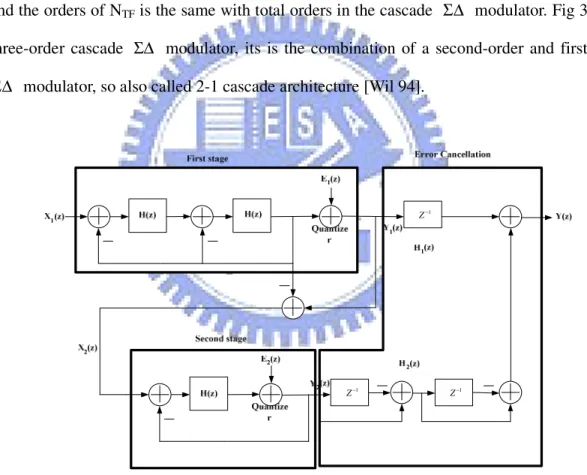
MASH (Multi-stage noise shaping) architecture is also called cascade architecture, which is a method that cascades several low order loops modulator in order to get high order noise shaping effect. The fundamental ideal of MASH is delivering quantization noise of front stage to input of next stage, and combining the digital outputs of all the stages with proper transfer function in digital domain, only the quantization noise of last stage will appear at the output, and the orders of NTF is the same with total orders in the cascade Σ∆ modulator. Fig 3.7 is a
three-order cascade Σ∆ modulator, its is the combination of a second-order and first-order Σ∆ modulator, so also called 2-1 cascade architecture [Wil 94].
1 − Z 1 − Z −1 Z
Fig. 3.7 2-1 architecture MASH Σ∆ modulator
From Fig. 3.7, we can derive the first stage output Y1(z) can be represented as
Y1(z) = z-2X1(z) + (1-z-1)2E1(z) (3.16)
Output of second stage Y2(z) is as
and overall output of MASH Y(z) is as
Y(z) = H1(z)Y1(z) + H2(z)Y2(z) (3.18)
and we can say that second stage input X2(z) is almost the same with E1(z), in order to
eliminate first stage quantization noise E1(z), from (3.16) ~ (3.18), we can define the error
cancellation functions H1(z) and H2(z) as
H1(z) = z-1 (3.19)
H2(z) = (1-z-1)2 (3.20)
From (3.16)~(3.20), E1(z) can be eliminated, and second stage quantization noise E2(z) is
shaped by third-order noise shaping function, and the MASH output Y(z) is as
Y(z) = z-3X1(z) + (1-z-1)3E2(z) (3.21)
The most significant advantage of this architecture is that stability is not an issue, because it is composed by several low-order systems, and the quantization noise will not be amplified stage by stage, so its stability is good. Most important, the noise shaping function is equivalent as high order Σ∆ modulator, so it is popular in recent publications [Rio 04][Vle 01]. However, there also have some drawbacks of this topology; it is sensitive to the circuits’ imperfections, such as finite DC gain of OTA, variance of integrator gain due to capacitor mismatch and non-zero switch resistance. These are all practical considerations when we design a MASH architecture Σ∆ modulator [Gag 03].
3.6 Multi-bit Quantizer Sigma-Delta Modulator
The demands of high resolution and high bandwidth ADC are more and more in recent years. In a high signal bandwidth, OSR of Σ∆ ADC can’t be too high, and the peak SNR of a Σ∆ modulator with such limited OSR can’t satisfy of high resolution applications, if we use higher order architecture, then the performance will degrade due to instability. So the most general method to increase performance is to use multibit quantizer. The most obvious advantage of using multibit quantizer is that the distance between quantizer level VLSB in (2.4)
is much smaller due to increasing of B, and according to (2.3), the power of quantization noise is attenuated. Fig. 3.8 is the results of theoretical peak SNR of Σ∆ modulator versus oversampling ratio, with different order and quantizer bits, it is noted that peak SNR of the same OSR is increase 6 dB with each additional bit number in quantizer, and at low OSR, low order higher bit number architecture has equivalent performance as high order architecture. This result is usable for high bandwidth applications, and the power consumption of digital circuit in Σ∆ modulator is reduced due to lower sampling rate [Pel 99].
0 50 100 150 200 250 300 20 40 60 80 100 120 140 160 OSR S N R O2B1 O2B2 O2B3 O3B1
Fig. 3.8 SNR vs. OSR with different quantizer bit number
Because of using multi-bit quantizer, so we also need to use multi-bit DAC(Digital-to Analog Converter) to transfer the digital output to analog signal, and feed it back to integrator. The most significant disadvantage is the non-linearities introduced by multi-bit DAC can degrade the performance of Σ∆ converter, like Fig. 3.9. It is a linear model of multi-bit Σ∆ modulator, where E(Q) and E(D) represent the quantization noise and feedback DAC noise respectively. The values of these capacitor elements in DAC will not equal to ideal values that we need, it is due to process variation, typical value of mismatch in modern CMOS technology is about 0.05% ~ 0.5%. In recent years, so many researches are make efforts on
reduce DAC noise due to mismatch, such as trimming [Nor97], Dynamic element matching(DEM)[Mil 03][Reb 90], although trimming is effective, but it has a expensive production step. So, DEM becomes more and more popular because of its efficiency and cheaper cost.
H(z)
X(n) Y(n)
Multi-bit Quantizer Discrete time Filter
Multi-bit D/A
E(Q)
E(D)
Fig. 3.9 Multi-bit architecture
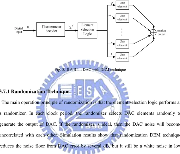
3.7 Multi-bit Sigma-Delta Modulator use DEM Technique
Dynamic element matching is a different approach to decrease the DAC noise, it is used to improve the linearity of pure DACs [Pla 79], but now it is most used in inner DAC of multi-bit Σ∆ modulator. A DAC with DEM technique is illustrated in Fig. 3.10, B
2 bits thermometer code is put into the element selection logic block, and the function of element selection logic is try to select DAC elements in such way let the errors introduced by DAC average to zero for several operation periods. Because the DEM block is located in feedback loop, so its delay must be very small prevent to degrade the performance of Σ∆ converter, therefore the algorithm used in the DEM block must be simple. There are several techniques of DEM, such as Randomization [Car 89], Clocked Averaging (CLA) [Pla 79], Individual Level Averaging (ILA) [Che 95], Data Weighted Averaging (DWA) [Bai 95], Randomization
is the first approach to use DEM technique in Σ∆ ADC, and DWA offers a good performance to reduce DAC error, in this section, an overview introduction of these two algorithms will be presented, and the operation principle of them will be explained.
1 2B− 1 2 B 2 B 2
Fig. 3.10 A B-bit DAC with DEM technique
3.7.1 Randomization Technique
The main operation principle of randomization is that the element selection logic performs as a randomizer. In each clock period, the randomizer selects DAC elements randomly to generate the output of DAC. If the randomizer is ideal, then the DAC noise will become uncorrelated with each other. Simulation results show that randomization DEM technique reduces the noise floor from DAC error by several dB, but it still be a white noise in low frequency. Fig. 3.12 is the output spectrum of a second-order Σ∆ modulator with a 0.1% capacitor mismatch, it is notable that the noise floor of randomization DEM is lower than that without any calibration technique in the feedback DAC.
3.7.2 Data Weighted Averaging (DWA)
DWA is a efficiently method to reduce DAC mismatch noise, it uses one register to remember the capacitor last time used, and always points to the first unused unit capacitor in this clock, so DWA rotates through all the unit capacitors such that all capacitors are used at the maximum possible rate. From this algorithm, each elements is used the same number of
times in long interval, this ensures that the errors caused by the DAC average to zero quickly. In Fig. 3.11, it is a 4-bit DAC and the shaded boxes are the number of 1’s in the thermometer code. Assumes that the input codes sequence is 8, 8, 10, 9, 10, 10, 11, 11, 12, 11, 14, 11, 14, 13, 12, 15... Fig. 3.12 is the simulation results of a third order Σ∆ modulator, we can see that without DEM has highest noise floor and DWA works as a first order noise shaping function of DAC noise, ideal DAC only with quantization noise has third-order noise shaping.
Fig. 3.11 Operation principle of the DWA algorithm
10-3 10-2 10-1 -200 -180 -160 -140 -120 -100 -80 -60 -40 -20 0 60 dB/decade P S D Normalized Frequency No DEM DWA ideal DAC
Fig. 3.12 Output spectrum with three kinds of DAC
Another consideration is the sub-ADC(quantizer) of the Σ∆ modulator, we usually use Flash A/D as the multi-bit quantizer because of its high speed, but Flash A/D has a significant disadvantage is that the number of comparators of it is proportional to 2B. That means a 6 bit quantizer needs 64 comparators, the occupied area of comparator may not much, but in modern SOC applications, the problems of power and area are important, so it becomes one
limitation of multi-bit quantization.
Σ∆ A/D converter is attractive for high resolution application, for higher signal bandwidth, we increase system order to raise SNR, but it still have stability problem. So people develop MASH and multi-bit architecture to improve its performance. Finally, we classify they into low order, high order, MASH and multi-bit four kinds of architecture, and compare their advantage and disadvantage as Fig. 3.13 [Med 99]
Σ∆
Fig. 3.13 Comparison of Σ∆ modulator architectures
3.8 Decimator
In Σ∆ A/D converter, digital decimator is used to process digital signal of the quantizer output, the high speed data word after oversampling modulation can’t be used directly. Because there have original signal and quantization noise among it, so the main function of decimator is to convert the oversampled B-bit output words of the quantizer at a sampling rate of fs to N-bit words at Nyquist rate of input, and removes the noise out of signal band. In order to prevent the noise introduced by other frequency, the decimator filter must have very
flat signal pass-band, and sharp transition region and enough signal attenuation in stop band. Two-stage decimator is used in a general situation, because that single stage decimator is difficult to convert sampling rate to Nyquist rate in 1 time and without degrading SNR. In the first stage, we can down-sample the sample frequency to 2~4 times of Nyquist frequency, and in the second stage, we can use IIR or FIR filter that have high linearity [Nor 97]. For a large OSR, multi-stage decimator is used.
3.9 Performance Metrics for a
Σ∆Modulator
In order to understand the performance merits used to specify the behavior of Σ∆ modulator, several specifications concerning the performance are discussed [Gee 02].
․Signal to Noise Ratio: The SNR of a data converter is the ratio of the signal power to the noise power, measured at the output of the converter for a certain input amplitude. The maximum SNR that a converter can achieve is called the peak SNR.
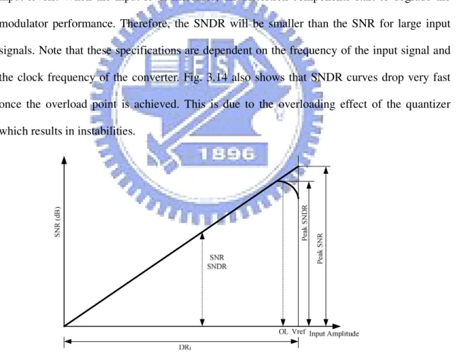
․Signal to Noise and Distortion Ratio: The SNDR of a converter is the ratio of the signal power to the power of the noise and the distortion components, measured at the output of the converter for a certain input amplitude. The maximum SNDR that a converter can achieve is called the peak SNDR.
․Dynamic Range at the input: The DRi is the ratio between the power of the largest input signal that can be applied without significantly degrading the performance of the converter, and the power of the smallest detectable input signal. The level of significantly degrading the performance is defined as the point where the SNDR is 6 dB bellow the peak SNDR. The smallest detectable input signal is determined by the noise floor of the converter. ․Dynamic Range at the output: The dynamic range can also be considered at the output of
the converter. The ratio between maximum and minimum output power is the dynamic range at the output DRo, which is exactly equal to peak SNR.
․Effective Number of Bits: ENOB gives an indication of how many bits would be required in an ideal quantizer to get the same performance as the converter. This numbers also
includes the distortion components and can be calculated from (2.6) as 02 . 6 76 . 1 ENOB= SNR− (3.22)
․Overload Level: OL is defined as the relative input amplitude where the SNDR is decreased by 6dB compared to peak SNDR
Typically, these specifications are reported using plots like Fig. 3.14. This figure shows the SNR and SNDR of the Σ∆ converter versus the amplitude of the sinusoidal wave applied to the input of the converter. For small input levels, the distortion components are submerged in the noise floor of the converter. Consequently, the SNDR and SNR curves coincide for small input levels. When the input level increases, the distortion components start to degrade the modulator performance. Therefore, the SNDR will be smaller than the SNR for large input signals. Note that these specifications are dependent on the frequency of the input signal and the clock frequency of the converter. Fig. 3.14 also shows that SNDR curves drop very fast once the overload point is achieved. This is due to the overloading effect of the quantizer which results in instabilities.
4
Models of Sigma-Delta Modulator Noises
and Power
Proposing an optimization algorithm for searching design parameters which maximize Σ∆ ADC SNR while minimize power consumption, is one of the primary purposes of this paper. Related model completeness determines success of this goal. The Σ∆ modulator nonidealities are categorized into five parts in this chapter; finite OTA gain error, thermal noise, settling error, multi-bit DAC noise, and jitter noise. All nonideality models are expressed in noise power form, which can directly add to ideal quantization noise power. All noise power models discussed in the following are based on the integrator scheme, as shown in Fig. 4.1. In Fig. 4.1, C is the unit capacitor whose capacitance value is u
B S
C
2
. The power consumption model is presented as the last part of this chapter.
I C I C S C ( B )X 1 2 − (B )X 1 2 − INP V INN V REFN V REFP V REFN V REFP V DAC DAC u C u C u C u C S C
4.1 Finite OTA Gain Error
Finite OTA Gain is an important error when we analyze a real integrator. Typical value of OTA gain is about 50 ~ 80 dB in modern CMOS technology. For a general single-loop n th order Σ∆ modulator with finite OTA gain A0, the modified quantization noise is expressed
as [Med 99]:
(
)
(
)
⋅ − ⋅ ⋅ + ⋅ + ⋅ ∆ ≅ − − + 2 1 2 2 2 1 1 2 2 2 .) (mod 1 2 1 2 12 n n n n Q OSR n n π A a OSR n π P AV Q P P + = (4.1) where PQ is the original quantization noise, and ∆ is the quantizer step size. The PAV in (4.1)is due to finite OTA gain, and can be considered as an additive quantization noise power. It can be verified using (4.1)that, for a single-loop topology, A = 50 dB is sufficient to avoid SNR degrades, in the sense that a higher A0 would not significantly reduce.) (mod
Q
P .
4.2 Thermal noise (Switch, OTA, Reference circuits)
There are three thermal noise sources in the Σ∆ modulator, in MOS switches, OTAs and reference voltage. We will analyze them separately as follows.
For a fully differential implementation, the in band switch thermal noise during the sampling phase results in output noise power [Med 99]
⋅ = S 1 C 4kT 1 OSR Psw (4.2)
where k is Boltzman constant and T is the absolute temperature. Additional thermal noise is introduced by the switches during the integration phase, resulting in the output noise power [Gee 02]
⋅ ≅ S 2 C 4kT 1 OSR Psw (4.3) Since the thermal noise voltages introduced during these two phases are uncorrelated, the total output switches thermal noise power from the switched capacitor integrator is
⋅ ≅ + = S 2 1 C 8kT 1 OSR P P Psw sw sw (4.4)
Half of P is from the input branch, and the other half is from the DAC branch. sw
The OTA transistor thermal noise can be modeled as an equivalent noise source V at no OTA input shown in Fig. 4.2. In deep submicron process
gm1 kT 10 Vno ⋅ ≅α V2Hz [Gra 01], where α is a noise factor depending on OTA topology. In a two-stage OTA, α ≈2. During the sampling phase (Fig. 4.2(a)), the circuit looks like a voltage follower. However, due to OTA finite gain bandwidth, noise at V has an equivalent bandwidth, so thermal noise O power at integrator output in the sampling phase is
L OTA AC A samp P 4 kT 10 2 2 GBW V ) ( no samp ⋅ = ⋅ ⋅ ⋅ ≅ π α π (4.5) During the integration phase (Fig. 4.2(b)), the circuit looks like a non-inverting amplifier, with + + + + ≅ A GBW S S s R sC R sC a s 1 2 1 2 1 2 ) ( V V 1 no O (4.6)
where GBWA is the 3dB frequency of the non-inverting amplifier. Then the OTA noise
power at the first integrator output can be expressed as
df f POTA 2 no O 0 no V ( ) V V (int)≅
∫
∞ ⋅ (4.7)± ± B 2 × no V L C O V I C L C no V S C I C u C O V
(a) sampling phase (b) Integration phase Fig. 4.2 Equivalent circuits of sampling and integration phases
Finally, the total OTA thermal noise power at the Σ∆ ADC output can be obtained as
1 1 ( ( ) (int)) 2 1 OTA OTA OTA P samp P a OSR P ⋅ + ⋅ = ⋅ + ⋅ ⋅ ⋅ =
∫
∞ f df AC a OSR L 2 no O 0 no 2 1 ) ( V V V 4 kT 10 1 α (4.8)The reference voltage circuit is implemented by transistors, so the thermal noise device will appear at the reference circuit output and influence the system directly. Consider the bandgap reference circuit in Fig. 4.3 [Raz 01]. Reference output noise is nearly equivalent to OTA input referred noise [Raz 01], so we can express it as
gm1 kT 10 Vno 2 ⋅α = ≈ ref V . Different
integrator schemes can introduce reference noise in different ways [Gag 03][Mil 03][Gee 00]. We consider the case shown in Fig. 4.4, where this noise is introduced only in the sampling phase. If the reference noise is unbuffered, its noise power at the Σ∆ ADC output can be derived as S 2 0 2 2 S 2 2 2 RC 4 C R 4 1 1 ⋅ = + ⋅ =
∫
∞ OSR V df f V OSR P ref ref refπ
(4.9)We usually add buffers between the bandgap circuits [Pie 02] and the DAC paths. Denote the 3dB buffer bandwidth as BWb. If BW is smaller thanb
S RC 4 1 , the ref P in(4.9)is changed to be
OSR BW V P b ref ref 2 2 ⋅ ⋅ = π (4.10) If BWbis larger than S RC 4 1 , the ref P in(4.9)is applied. dd
V
Fig. 4.3 A bandgap voltage reference circuit
2 ref V ± B 2 × u
C
uC
SC
IC
LC
inV
oV
Fig. 4.4 Equivalent circuit while considering reference voltage noise
4.3
Settling Problem
As Σ∆ modulator sampling frequency increases, and multi-bit quantization becomes a high resolution and high-speed application trend, the dynamic settling problem of switched capacitor integrator becomes a more dominant factor. Previous articles have mentioned the settling error [Mal 03][Gri 02][Rio 00]. References [Mal 03] and [Rio 00] provide behavior
models, which are tedious and integrate poorly with noise-power models of other noises or errors. The noise-power model of [Gri 02] is very primitive since it assumes the pdf (probability density function) settling error is uniformly distributed, and does not consider multi-bit quantization. We only consider the integrator at the first stage. Settling errors at later stages are less influential due to noise shaping.
Now consider a switched capacitor integrator in Fig. 4.5. Assume the MOS switch has an on-resistance R, and gm1 is the transconductance of OTA. Let the output parasitic capacitor
I L C
C ≅η⋅ , where η is the percentage of bottom plate parasitic, assumed to be 20% [Rab 99]. In Fig. 4.5(a), the voltage VS represents the difference between the sinusoid input signal and the feedback signal from DAC. It is sampled by CS, so CS is charged in the half clock
period 2 T to the voltage VCS: )] 2 exp( 1 [ 1 τ ⋅ − − ⋅ =V T VCS S (4.11) where τ1=R⋅CS is the time constant in the input branch. So the setting error during the
sampling phase is:
) 2 exp( 1 1 τ ε ⋅ − ⋅ =VS T (4.12) S C S V I C L C VO S V 1 gm I C L C S C R O V S C DAC
(a) Sampling phase (b) Integration phase Fig. 4.5 Switched capacitor integrator diagrams
In order to obtain settling noise power during the sampling phase from(4.12), we need to find the VS statistical property. Simulations results (using SIMULINK) on a second-order Σ∆ modulator with a1=0.5, a2 =2, 10-level quantization, reference voltage Vref =±1, and a full scale sinusoidal input signal, are shown in Fig. 4.6. The result is close to a Gaussian
distribution. Therefore, we assume VS is Gaussian distributed with a zero mean. The standard deviations
σ
VS of VS under different quantizer levels are tabulated in Table 4.1. We observed that when the quantizer level N increases,σ
VS decreases. From this table, therelation between standard deviation
σ
VS and quantizer levelsB
2 can be approximated by 2B⋅σvs≈1.4⋅Vref (4.13)
Fig. 4.6 Simulated results of VS distribution
Std. deviation (σVS) Variance Quantizer level (N) Bit number (B) 0.706 0.498 2 1 0.476 0.227 3 1.585 0.282 0.080 5 2.322 0.198 0.040 7 2.808 0.152 0.023 9 3.17 0.124 0.016 11 3.46 0.047 0.002 31 4.95
TABLE 4.1 Standard deviations of VS vs. different quantizer bit numbers
The settling noise can reasonably assumed to be white, and its power spectral density constant and distributed over (− fS 2, fS 2) as:
exp( ) 2 V 4 . 1 1 1 2 ref 1 τ ε T f S B S − ⋅ ⋅ ⋅ = (4.14)
Due to oversampling, noise power can be obtained by integrating(4.14)in the signal band ) , (−fB fB , which is: exp( ) 2 V 4 . 1 1 1 2 ref 1 τ ε T OSR P B ⋅ − ⋅ ⋅ = (4.15)
Next, we consider the integration phase shown in Fig 4.5(b), where the
2
B unit capacitors are combined intoS
C , and the
2
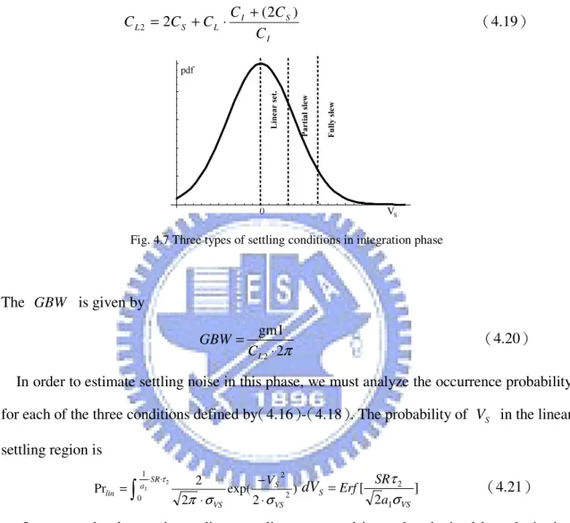
B DAC switches are neglected. The charge stored in sampling capacitor will be added to the integration capacitor and this charge current is supplied by OTA. So when the slew rate and gain bandwidth are not large enough, the settling errorε
2 will be produced. The statistical properties of VS have been summarized in Table I. Then, according to Fig. 4.7, three types of settling conditions can happen in the integrator output during this phase, and the corresponding voltage errors of these three conditions are [Mal 03]:1. Linear settling: When the initial change rate of the integrator output voltage (V ) is O smaller than the OTA slew rate (SR).
) 2 exp( 2 1 2 τ ε ⋅ − ⋅ ⋅ =a VS T , when 2 1 1 0< < ⋅SR⋅τ a VS (4.16)
2. Partial slewing: The initial change rate of V is larger than O SR, but it gradually decreases until it is below the slew rate.
1) 2 exp( 2 2 1 2 2 − − ⋅ ⋅ ⋅ ⋅ = τ τ τ ε T SR V a SR S , when 1 2 2 1 ) 2 ( 1 a SR T V SR a ⋅ ⋅τ < S < +τ (4.17)
3. Fully slewing: The initial change rate of V is larger than O SR, and it maintains above SR in the 2 T interval. 2 1 2 T SR V a ⋅ S − ⋅ = ε , when ) 2 ( 2 1 τ + > T a SR VS (4.18)
where SR is the slew rate of OTA, and
GBW Cs R GBW ⋅ ⋅ ⋅ ⋅ + = π π τ 2 2 1
constant in the integration phase, with GBW being the equivalent gain bandwidth in the integration phase. The capacitor loading in OTA output during this phase is heavier than in the sampling phase, and is [Gee 02]
I S I L S L C C C C C C 2 =2 + ⋅ +(2 ) (4.19) 9.5 10 10.5 11 11.5 0.2 0.4 0.6 0.8 1 F u ll y s le w P ar ti al s le w L in ear s et . S V
Fig. 4.7 Three types of settling conditions in integration phase
The GBW is given by π 2 gm1 2⋅ = L C GBW (4.20)
In order to estimate settling noise in this phase, we must analyze the occurrence probability for each of the three conditions defined by(4.16)(- 4.18). The probability of VS in the linear settling region is
∫
⋅ ⋅ ⋅ − ⋅ = 1 2 1 0 2 2 ) 2 exp( 2 2 Pr τ σ σ π SR a VS S VS lin V S dV ] 2 [ 1 2 VS a SR Erf σ τ = (4.21)Let ε2max be the maximum linear settling error, and it can be obtained by substituting
2 1 1 τ ⋅ ⋅ = SR a
VS into(4.16). Since VS is approximately Gaussian, it is reasonable to assume that the linear settling error in (4.16) also has a Gaussian distribution in
(
−ε2max,ε2max)
. So the average linear settling noise power in the integration phase is approximately2 2 2 2 max 2 ) 2 exp( 9 1 9 − ⋅ = ≈ τ τ ε T SR Plin (4.22)