國
立
交
通
大
學
資訊科學與工程研究所
碩
士
論
文
全數位鎖相迴路之
相位追蹤與頻率追蹤控制器設計
The Study of Phase Tracking and Frequency Search for Single
DCO-based ADPLL Designs
研 究 生:李峻榮
指導教授:許騰尹 教授
全數位鎖相迴路之相位追蹤與頻率追蹤控制器設計
The Study of Phase Tracking and Frequency Search for Single
DCO-based ADPLL Designs
研 究 生:李峻榮
Student : Jyun-Rong Li
指導教授:許騰尹
Advisor : Terng-Yin Hsu
國 立 交 通 大 學
資 訊 科 學 與 工 程 研 究 所
碩 士 論 文
A Thesis
Submitted to Institute of Computer Science and Engineering College of Computer Science
National Chiao Tung University in partial Fulfillment of the Requirements
for the Degree of Master
in
Computer Science
June 2006
Hsinchu, Taiwan, Republic of China
全數位鎖相迴路之相位追蹤與頻率追蹤控制
器設計
學生:李峻榮 指導教授:許騰尹 博士
國立交通大學資訊科學與工程研究所 碩士班
摘要
現代的系統單晶片(SoC) 需要晶片內部的時脈產生器用以產生不同的頻率來給予內部 其他的子系統使用,一般而言以鎖相迴路為基礎的時脈產生器來達到此目的。為了減少抖 動量及增加迴路的穩定度,必須依照輸出頻率及倍數來調整設計參數,然而現今的類比鎖 相迴路需要較長的設計週期。 相較而言以全數位的方式實作鎖相迴路更能節省系統晶片整合的成本。然而現今大部 分的數位鎖相迴路仍是以追蹤頻率為主要考量,如此之下在部分與相位誤差有關的應用 中,全數位鎖相迴路便不適用於此應用當中。在本文中將提出以相位為主的追蹤演算法, 使全數位鎖相迴路更能適應於各類應用當中。此外在僅使用單一數位控制震盪器的前提 下,提出一個低輸出擾動,高效率的追蹤演算法。為了達到此目的,一個便於分析相位頻 率分析的相位狀態圖將被提出。為了解決雙數位控制震盪器所導致的不匹配問題,根據此 相位狀態圖,一個類數位訊號處理器的架構將被提出。綜合以上所有,一個全新可移植整 合的全新架構的全數位鎖相迴路將被提出在此篇論文當中。The Study of Phase Tracking and Frequency
Search for Single DCO-based ADPLL
Designs
Student:
Jyun-Rong
Li Advisor:
Dr.
Terng-Yin
Hsu
Institute of Computer Science and Engineering College of Computer
Science
National Chiao Tung University
Abstract
Modern system-on-a-chip (SoC) processors often require on-chip clock generation and multiplication to produce several unrelated frequencies for other sub-systems. The PLL is common way of frequency multiplication to accomplish the task. In order to minimize the jitter and insure the stability for each output frequency, the design parameters need to change according to the output frequency and multiplication factors. Conventional analog skills suffer from long design cycle.
In SoC design, it can save more time when we use the all-digital skill to implement the PLL. However, most of current ADPLL controlled only discuss with the frequency tracking. Under this situation, the ADPLL cannot meet the requirements of some applications, which is depended on the phase error. This thesis provides a phase tracking based algorithm, thus the proposed ADPLL can be portable in varied applications. Furthermore, the proposed tracking algorithm has high efficiency and low output jitter. The proposed ADPLL with single DCO solves the mismatch problem in clock pair architecture. Moreover, DSP based architecture is proposed to provide a programmable and stable ADPLL. In order to realize All-Digital PLL, new approaches be presented to offer portable, full-integration and low-jitter frequency synthesizer in digital VLSI.
Acknowledgement
This thesis describes research work I performed in the Integration System and Intellectual Property (ISIP) Lab during my graduate studies at National Chiao Tung University (NCTU). This work would not have been possible without the support of many people. I would like to express my most sincere gratitude to all those who have made this possible.
First and foremost I would like to thank my advisor Dr. Terng-Yin Hsu for the advice, guidance, and funding he has provided me with. I feel honored by being able to work with him.
I am very grateful to all members of ISIP Lab for their support and suggestions.
Finally, and most importantly, I want to thank my parents for their unconditional love and support they provide me with. It means a lot to me.
Table of Contents
page
摘要 . . . i Abstract . . . .ii Acknowledgement . . . .iii Chapter 1 Introduction . . . 1 1.1. Thesis Background . . . .1 1.2. Thesis Motivation . . . .1 1.3. Thesis Organization . . . .2Chapter 2 Overview of Phase-Locked Loop. . . .3
2.1. Basic Concept of PLL . . . .3
2.2. Digital Phase-Locked Loop . . . 3
2.2.1. ADPLL with fixed High-speed Clock . . . .4
2.2.2. Adaptive Gain Control with Full-custom DCO . . . .4
2.2.3. Standard Cell-based ADPLL . . . .5
Chapter 3 Phase Tracking and Frequency Search Algorithm . . . 7
3.1. Basic Concept of Phase Tracking Algorithm . . . 7
3.2. The Definition of Phase Tracking and Frequency Search. . . 9
3.3. Challenges of Phase Tracking and Frequency Search. . . 12
3.4. The Proposed Phase Tracking and Frequency Search Algorithm . . . 13
3.4.1 Frequency and Phase Acquisition. . . .13
3.4.2. Coarse Tracking Algorithm. . . . 15
3.4.3. Fine Tracking Algorithm. . . 16
3.5. HDL Jitter Model . . . .18
3.6. Jitter Reduction . . . 19
3.6.1. Types of Jitter . . . 19
3.6.2. Tradeoffs Between Loop Filter Parameters. . . 19
3.7. Simulation Results . . . .21
Chapter 4 The proposed ADPLL Architecture. . . .26
4.2. Circuit Designs . . . .26
4.2.1. Digital-Controlled Oscillator (DCO) . . . .26
4.2.2. TDC . . . 27
4.2.3. HSPD with Pulse Amplifier. . . .28
4.2.4. Frequency Error Detector (FED) . . . 28
4.2.5. Flag . . . .29
4.2.7. Register . . . 29
4.2.8. Delay Time Selector . . . 29
4.2.9. Controller . . . .30
4.2.10. DCO Controlled Word Buffer (DCWB) . . . .30
4.2.11. Frequency Divider . . . 30
Chapter 5 Conclusion and Future Work . . . 31
5.1. Conclusion . . . 31
5.2. Future Work . . . .31
List of Figures
page
Fig. 2.1 Basic block diagram of PLL . . . 3
Fig. 2.2 Basic concept for estimating input’s phases and frequencies . . . .4
Fig. 2.3 The structure of cell-based digital controlled oscillator . . . 5
Fig. 2.4 the binary search ADPLL controller . . . .5
Fig. 2.5 the structure of time-to-digital converter . . . 6
Fig. 3.1 The simple phase tracking process . . . 8
Fig. 3.2 the modified phase acquisition process . . . .8
Fig. 3.3 the corresponding waveform at position a and b . . . .10
Fig. 3.4 . . . 10
Fig. 3.5 . . . 12
Fig. 3.6 . . . 12
Fig. 3.7 The scenario of phase tracking & frequency search . . . 13
Fig. 3.8 The flow chart of proposed algorithm . . . .13
Fig. 3.9 The first cycle of frequency acquisition . . . .14
Fig. 3.10 The relation between TDC and DCO control word . . . .14
Fig. 3.11 The basic steps of the proposed algorithm . . . 14
Fig. 3.12 the proposed algorithm . . . .15
Fig. 3.13 all situations by the proposed algorithm . . . .15
Fig. 3.14 . . . 17
Fig. 3.15 . . . 17
Fig. 3.16 . . . 18
Fig. 3.17 Period jitter . . . 19
Fig. 3.18 Cycle-to-cycle jitter. . . 19
Fig. 3.19 Long-term jitter. . . 19
Fig. 3.20 . . . 20
Fig. 3.21 The structure of filter . . . 21
Fig. 3.22 . . . 21
Fig. 3.23 . . . 22
Fig. 3.25 . . . 23
Fig. 3.26 . . . 24
Fig. 4.1 The proposed architecture . . . .26
Fig. 4.2 The proposed DCO. . . .27
Fig. 4.3 The problem of inverter delay line . . . .27
Fig. 4.4 The proposed pulse amplifier . . . .28
Fig. 4.5 The corresponding waveform of proposed pulse amplifier . . . .28
Fig. 4.6 The frequency error detector. . . 29
Chapter 1
Introduction
1.1.
Thesis Background
Traditionally, Phase locked loop (PLL) based clock generators for microprocessor are common way of frequency multiplication from a low-frequency reference clock, typically from quartz oscillator. They are often applied to communication applications, such as: frequency synthesizer, clock multiplier, Clock and Data Recovery (CDR) circuit, and clock de-skew applications. As VLSI technology grows up rapidly, the advance of semiconductor process enables the successful realization of system-on-chip (SoC). Such applications often require on-chip clock generation and multiplication to produce several unrelated frequencies for digital signal processing, I/O interfaces. The diversity of SoC applications has led to diversity in operating frequencies and multiplication factors in PLL.
Because of the design of PLL-based clock generator is a trade-off among jitter performance, frequency and phase resolution, lock-in time, power consumption, area-cost, circuit complexity and design time. To provide ample flexibility for a variety of applications is a big challenge for PLL design. It often needs to redesign the PLL for target application.
In addition, most PLL design use mixed signal and full custom design techniques, which can not be fully in digital environment. Due to time-to-market issue, the design cycle remains the same or even shorter. Thus in System-on-Chip (SoC) design, each module had better to be reusable and process portable, so that the total design time can be reduced. As a result, how to design these PLLs in a more efficient way becomes more and more important in these days.
1.2.
Thesis Motivation
All-digital and cell-based approach is preferred for SoC application over their analog counterparts. Firstly, traditional analog loop filter costs a lot of chip areas. Using digital loop filters gives benefits such as programmable parameters, robustness against noise, and also the ability to design higher order filters without much extra power consumption and area penalty. Secondly, analog component are vulnerable to DC offset and drift phenomena that are not present in equivalent digital implementations. Thirdly, the loop dynamics of analog PLLs are quite sensitive to process technology scaling, whereas the behavior of digital logic remain unchanged with scaling, so it requires much more significant redesign effort to migrate analog PLLs to a new technology node than all-digital and cell-based approach. For above
reason, all-digital and cell-based approach can reduce significantly both time and design complexity by using hardware-description language, and the final circuit layout to be generated by an auto placement and routing (APR) tools.
In recently years, ADPLL became more attractive since they yield better testability, programmability, stability and portability over different processes. But most ADPLL design in recently years separate phase lock into the phase acquisition and frequency acquisition to enhance each individually. This way will reduce the period jitter and the cycle-to-cycle jitter, thus they gat a good jitter performance. But this kind of method is not suitable in some applications, like a graphics card driving a CRT, because of the terrible long-term jitter and phase error. Furthermore, most designs of ADPLL use two DCOs to reduce the design complexity; because DCO is working at the highest frequency compare with other modules in design generally, this will lead large power consumption. And dual DCO architecture has mismatch problem between inner clock and output clock. Thus how to design a fast-locking ADPLL with one DCO and still have good jitter performance for widely applications in a short design time is the challenge in ADPLL design.
1.3.
Thesis Organization
The organization of this thesis is as follows:
In chapter 1, we introduce that difference clock domains are required in a SoC chip. Using portable clock generator to replace conventional PLL is feasible.
In chapter 2, we give an overview of PLL related techniques for the proposed ADPLL. The different PLL approaches are discussed.
In chapter 3, the proposed algorithm is introduced. A detailed description of the idea and simulation are given.
In chapter 4, we utilize the proposed ADPLL described in chapter 3. Detailed structures are then discussed.
In chapter 5, some concluding remarks will be derived from this research. Finally, we describe several design issues that needed to be further explored in the near future.
Chapter 2
Overview of Phase-Locked Loop
As shown in chapter 1, numerous applications, such as video graphics card, microprocessor and telecommunication system, require a clock synthesizer. Several methods exist for realizing frequency multiplication: phase locked loop (PLL), delay locked loop (DDL), and direct digital synthesis (DDS). Each of these methods has advantages and disadvantages for frequency multiplication. DLL approach may offer better jitter performance than PLL approach; but it is not suitable for wide multiplication range applications. The direct digital synthesis applied accumulator and D/A converter mechanism for frequency synthesis. Therefore, we only focus on the PLL approach in this work.
The organization of this chapter is as follows. Section 2.1 describes the basic concept of analog PLL. The architecture and algorithm of different digital PLL are discussed in section 2.2.
2.1.
Basic Concept of PLL
A phase-locked loop (PLL) is combined with phase detector (PD), voltage controlled oscillator (VCO), and loop filter (LF). The basic block diagram is shown in Fig. 2.1, where PLL is a negative feedback control loop. The PLL's characteristics are determined by characteristics of PD, VCO and, LF. Its performances are taken careful of two kinds, one is the phase error, the difference between the input phase and output phase; and the other is the frequency range, what range over which it will acquire lock. As a result, PLL can be regarded as a tracking phase system.
Fig. 2.1 Basic block diagram of PLL
2.2.
Digital Phase-Locked Loop
All analog building blocks are replaced with digital representations in all-digital PLL. Many different DPLL are discussed in literature. This section discusses some DPLL architectures as below: (1) ADPLL with fixed high-speed clock, (2) An adaptive gain control with full-custom DCO, (3) Standard cell-based ADPLL.
2.2.1. ADPLL with fixed High-speed Clock
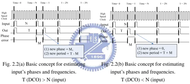
It is assumed that a high-speed clock is used as reference timing, and all signals must be referred to this clock. Generally, the high-speed clock is faster than input at least 10 times to achieve better performance. The proposed algorithm [1] is illustrated in Fig. 2.2(a) and Fig. 2.2(b) for two conditions. Fig. 2.2(a) shows the case of DCO’s frequency (1/period) which is slower than input signals, i.e. T (DCO) > N (input). Fig. 2.2(b) shows the other case of DCO’s frequency which is faster than input signal, i.e. T (DCO) < N (input).
Fig. 2.2(a) Basic concept for estimating input’s phases and frequencies.
T (DCO) > N (input)
Fig. 2.2(b) Basic concept for estimating input’s phases and frequencies.
T (DCO) < N (input)
2.2.2. Adaptive Gain Control With Full-custom DCO
If the high-speed clock is available, such as in SoC, and the target operation’s speed is not very high, then DCO with fixed high-speed clock can be the choice. However, it may consume large power due to high-speed clock operation. So, an ADPLL [2] was proposed as a frequency synthesizer for microprocessor that did not require external fixed high-speed clock. The ADPLL has a 50 cycle phase lock, has a gain mechanism independent of process, voltage, and temperature.
It separated the frequency acquisition and phase acquisition. A high-resolution frequency comparator with matching delay line was utilized to enhance frequency accuracy. An anchor register is needed to store the baseline frequency. After frequency acquisition is completed, the ADPLL starts to trace the phase relation between reference clock and DCO clock. The phase tracking process was performed with a phase control algorithm and a phase detector.
After the frequency acquisition and phase acquisition, the ADPLL enters phase and frequency maintaining process. However, the cost of this chip area is extremely high due to DCO. Those DCO designs were required to be with full-custom layout. The full-custom DCO make it difficult for porting to difference process as design specification to be changed.
2.2.3. Standard Cell-based ADPLL
To improve performance and decrease costs of system integration, much more requirements and constraints must be taken into account in implementation. For advances and improvements of digital VLSI, all digital methodology has good abilities to satisfy above requirements of computer and communication applications in recent years. A major problem of traditional direct DCO synthesis method is the highly technology dependence. So, the portable design is an important issue in digital VLSI to improve system-on-chip (SOC) turnaround. The key issue is that all of the elements are designed form standard cell library without fully-custom layout. A high-resolution cell-based DCO is shown in Fig. 2.3, which includes two major parts. One is the inverter chain to perform coarse searches, and the other is the fine module. Hence, the operating range is determined by number of cascaded inverters, and the resolution is decided by scale of fine module. So, how to enhance the fine module accuracy is a big challenge of cell-based PLL design.
mux . . . Fine module Coarse module DCO clock
DCO controlled words
Fig. 2.3 The structure of cell-based digital controlled oscillator
Fig. 2.4 the binary search ADPLL controller
There are two common algorithms to realize the controller: one is binary search based ADPLL controller; the other is TDC-based fast-locking ADPLL controller. The ADPLL may have two DCOs for low output jitter associated with input reference. An average loop filter is necessary to filter out the rippling and produce smoother digital controlled word with less jumping.
The basic concept of binary search based ADPLL is a “Prune-and-Search” algorithm. Fig. 2.4 illustrates the frequency acquisition process. Whenever the frequency detector’s output changes from up to down or vice versa, the search step is divided by two. And after the search step reduces to one, the frequency acquisition is done. Then the ADPLL controller enters
phase acquisition and phase maintaining mode.
For fast-locking applications, lock-in time is the most critical design issue. Thus a time-to-digital converter (TDC) is used to quickly calculate the nearest control code for DCO to produce the desired frequency. TDC can convert the reference clock’s period information to multiples of delay cell’s delay time. Hence, ADPLL controller can use this information to quickly jump to the desired frequency band. And then ADPLL performs fine-turning to reduce the residual frequency error and phase error. As a result, the lock-in time can be reduced by adding TDC module. The basic structure of TDC is show in Fig. 2.5.
Counter
. . .
Latch & Encoder Latch
Input signal
Integrator Output
Fig. 2.5 the structure of time-to-digital converter
However, the controlled code may have small variations due to the following factors: Phase detector’s dead zone, DCO’s resolution. In phase acquisition process, Phase detector must provide correct phase relationship information about reference clock and divided output clock. The dead zone of phase detector will increase phase acquisition time and final phase error. To minimize the dead zone of Phase detector, several new phase detectors are proposed. The key component is the digital pulse amplifier. Increasing the sensitivity of pulse amplifier will increase the sensitivity of phase detector and increase accuracy of controller.
Chapter 3
Phase Tracking and Frequency
Search Algorithm
As discussion in chapter 2, most ADPLL lock-in process is separated in frequency acquisition and phase acquisition. By the TDC based or adaptive gain control algorithm, the PLL controller controls the internal oscillator’s output frequency to minimize frequency error. After frequency acquisition is completed, the PLL turns into phase acquisition and phase maintaining mode. The lock-in time of PLL is mainly determined by the frequency acquisition time, thus how to reduce frequency acquisition time is very important to a fast-locking PLL design.
In this chapter, a new phase tracking based algorithm will be proposed. Most previous ADPLL algorithms are frequency searching based algorithms. They may not meet for some applications that depend on phase error. Actually, it can achieve the function of ADPLL either by frequency acquisition or by phase tracking. By the phase tracking algorithm, we only need to focus on how to minimize the phase error; and frequency maintain is done. We don’t need to divider our algorithm into phase acquisition and phase & frequency maintaining modes. The proposed algorithm is flexible and very suitable for more applications.
The organization of this chapter is as follows. Section 3.1 describes the simple phase tracking process. Section 3.2 gives a new definition of phase tracking process. Section 3.3 explains the challenges of the phase tracking algorithm. The proposed algorithm is introduced in Section 3.4. Section 3.5 introduces the jitter model in this thesis. How to minimize the jitter is discussed in section 3.6. Section 3.7 gives the simulation result with verilog and matlab.
3.1.
Basic Concept of Phase Tracking Algorithm
The basic concept of phase tracking algorithm is to minimize the phase error according to the information phase detector provide. The simplest way is very similar to the method in section 2.2.1 but no high speed reference clock. Fig. 3.1 illustrates the phase acquisition process of PLL. If we assume the frequency error between reference clock and divided output clock is very small after frequency acquisition, and the phase error between reference clock
and divided output clock is . And we assume at time = t0, t1 and so on, the phase detector finds that divided output clock lags behind reference clock. The PLL controller will control the internal oscillator to speed up. Without high speed clock, we don’t know the value of
Δ
Δ , so we modify the DCO controlled words with a constant value.
Fig. 3.1 The simple phase tracking process
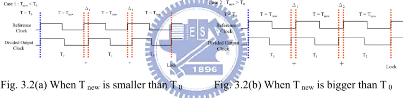
Clearly, this method is passive and slow. So we think about the other way to speed up phase tracking with TDC aided. Fig. 3.2 illustrates the modified phase acquisition process of PLL for two conditions. Because we have more information about phase error, the value and the direction, we can tune the DCO controlled word with variable value.
Δ1 Δ2 T0 T1 T2 Lock - -Case 1 : Tnew< T0 T = Tnew T = T0 T = Tnew T = Tnew Δ1 Δ2 T0 T1 T2 Lock + + Case 2 : Tnew> T0
T = T0 T = Tnew T = Tnew T = Tnew
Fig. 3.2(a) When T new is smaller than T 0 Fig. 3.2(b) When T new is bigger than T 0
This modified method is similar a phase & frequency maintain algorithm. If we assume that there exists a phase lock before, we get phase error due to the change of reference clock or incorrect DCO frequency. As show in Fig. 3.2(a), when the cycle time of reference clock changes from T0 to T new, the phase detector finds that divided output clock lags behind
reference clock, and the TDC tell us the value isΔ . So we subtract a corresponding value 1 ofΔ1from DCO controlled word and get new cycle time, T1.
1 0
1 T
-T = Δ (3-1)
After one reference clock cycle time, we get the phase errorΔ . Again, by subtracting the 2 DCO controlled word and getting a new DCO setting. The period time of new setting is T2.
2 1
2 T
Then we can calculate the correct cycle time of reference clock from equation (3-3), and set the corresponding setting into DCO controlled word.
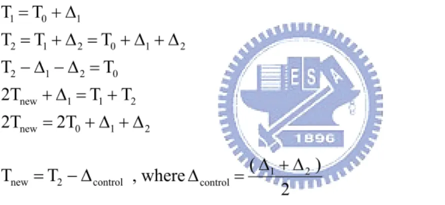
-2T T T 2T T T -T -T T -T T 2 1 0 2 1 1 new 0 2 1 2 2 1 0 2 1 2 1 0 1 Δ Δ = + + Δ = = Δ + Δ + Δ Δ = Δ = Δ = T
Tnew = 2+Δcontrol , where
2 ) ( 1 2 control Δ + Δ = Δ (3-3)
Fig. 3.2(b) shows the other case of reference clock which is slow than divided output clock. From equation (3-4), we still get the phase & frequency lock at third cycle.
2 1 0 new 2 1 1 new 0 2 1 2 2 1 0 2 1 2 1 0 1 2T 2T T T 2T T T T T T T T Δ + Δ + = + = Δ + = Δ − Δ − Δ + Δ + = Δ + = Δ + = T
Tnew = 2−Δcontrol , where (3-3)
2 ) ( 1 2 control Δ + Δ = Δ
But this method is still like other phase & frequency algorithm, which need a phase lock before; that means we need to do the phase acquisition process. So the performance of phase error will be limited by how small phase error that phase acquisition process can achieve is.
3.2.
The Definition of Phase Tracking and Frequency Search
In real situations, input information is very important for tracking or recovering desired signals correctly. In order to extract accurately and track immediately input information, it is necessary to estimate both phases and frequencies of input signals continuously. Obviously, the information from phase detector and TDC is still not enough to achieve minimum phase error; we need to find more information to reach the goal.
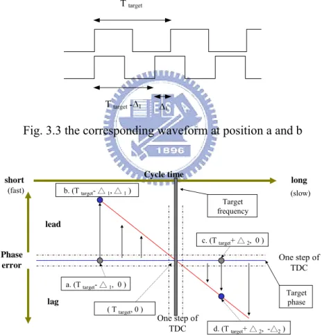
Fig. 3.4 illustrates the new definition of phase tracking & frequency search problem. The horizontal line means the cycle time of divided output clock or reference clock which is according to the scale of TDC. The vertical line represents the phase relation between divided
output clock and reference clock. The magnitude is according to the value of TDC, too. Fig. 3.4 illustrates the relation between phase error and frequency error. When initial phase error is zero and initial frequency error is zero, we denote this situation as (T target, 0), where T target
is the cycle time of reference clock. When initial phase error is zero and the cycle time of divided output clock is (T target -Δ1), we denote this situation as (T target - , 0). Fig. 3.4(a) shows that where the position at next cycle time while current phase error is zero and DCO controlled word is no change. When divided output clock is faster than reference at current cycle, like a: (T
1 Δ
target -Δ , 0), next position will be at b: (T 1 target -Δ ,1 Δ ) if we don’t change the 1
controlled word. It is very easy to been proven from Fig. 3.3. When divided output clock is slower than reference at current cycle, like c: (T target +Δ , 0), next position will be at d: (T 2
target + ,- ) if we don’t change the controlled word. Because both horizontal and vertical
line use the same scale, the oblique line will be . 2
Δ Δ2
o
45 −
Fig. 3.3 the corresponding waveform at position a and b
One step of TDC One step of TDC (slow) Cycle time Phase error lead lag short long (fast) Target phase Target frequency ( T target, 0 ) a. (T target- △1, 0 ) b. (T target- △1, △1) c. (T target+ △2, 0 ) d. (T target+ △2, -△2)
Fig. 3.4(a) Initial phase error is zero
Fig. 3.4(b) illustrates the situation when the initial phase error is not zero. It also can be proven by drawing its corresponding waveform.
One step of TDC One step of TDC Cycle time Phase error lead lag short long
Fig. 3.4(b) Initial phase error is not zero
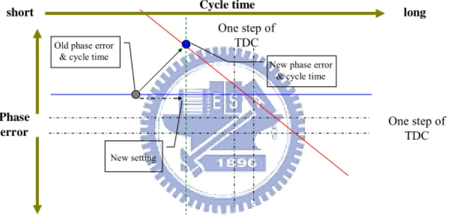
Fig. 3.4(c) illustrates the general condition when the initial phase error is not zero and DCO controlled word applies new setting at current cycle. This also can be proven by drawing its corresponding waveform.
One step of TDC One step of TDC New setting Cycle time Old phase error
& cycle time
New phase error & cycle time Phase
error
short long
Fig. 3.4(c) Initial phase error is not zero and DCO controlled word applies new setting It often waste a lot of time to drawing the waveform to explain the phase tracking & frequency search problem, and the waveform is usually hard to be understood. We transfer the phase tracking & frequency search problem into the other problem to deal with. The new problem we need to solve is shown in Fig. 3.5. The problem is how to reach the position of (T
target, 0) from any other position in Fig. 3.5. Obviously, the best solution is a straight line from
starting point to our goal, as show in Fig. 3.5(a). Actually, that is very hard to achieve it. The greedy solution may be a whirlwind-like curve, as show in Fig. 3.5(b). To solve this problem is to solve the phase tracking & frequency search problem. The following sections all base on the new definition to discuss.
One step of TDC One step of TDC Phase error long short lead lag ( T target, 0 ) One step of TDC One step of TDC Phase error long short lead lag ( T target, 0 )
Fig. 3.5(a) The best solution Fig. 3.5(b) The greedy solution
3.3.
Challenges of Phase Tracking and Frequency Search
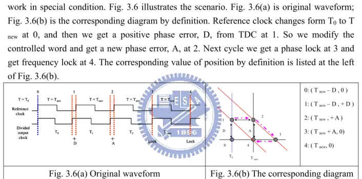
As discussion in section 3.1, the modified phase & frequency maintaining algorithm only work in special condition. Fig. 3.6 illustrates the scenario. Fig. 3.6(a) is original waveform; Fig. 3.6(b) is the corresponding diagram by definition. Reference clock changes form T0 to T new at 0, and then we get a positive phase error, D, from TDC at 1. So we modify the
controlled word and get a new phase error, A, at 2. Next cycle we get a phase lock at 3 and get frequency lock at 4. The corresponding value of position by definition is listed at the left of Fig. 3.6(b). D T0 T1 T2 Lock + +
T = T0 T = Tnew T = Tnew T = Tnew
A T = Tnew T new Lock 0 1 2 3 Reference clock Divided output clock 4 D T0 T1 T2 Lock + +
T = T0 T = Tnew T = Tnew T = Tnew
A T = Tnew T new Lock 0 1 2 3 Reference clock Divided output clock 4 D A T0 T new 2 1 0 3 4 0: ( T new – D , 0 ) 1: ( T new – D , + D ) 2: ( T new , + A ) 3: ( T new + A, 0) 4: ( T new, 0)
Fig. 3.6(a) Original waveform Fig. 3.6(b) The corresponding diagram What happen if there is no “really” phase lock before maintaining algorithm? The term “really” means how small the phase error is. This term will be limited by the dead zoon of phase detector. Fig. 3.7 shows the scenario in this situation. The path will be a close loop, and the magnitude of phase error and frequency error will be cyclic. It never achieves the “really” phase & frequency lock. Actually, most phase & frequency maintaining algorithms which are discussed in chapter 2 have the same problems even though phase acquisition algorithm and frequency acquisition algorithm are aided. This problem is due to the regularity of tracking process.
D A D A A D A A A-D D D 1 2 3 4 5 6 1: ( T new – A , +D ) 2: ( T new – (A-D) , + A ) 3: ( T new +D, + (A-D) ) 4: ( T new + A, -D)
5: ( T new + (A-D), -A)
6: ( T new -D, -(A-D))
Fig. 3.7 The scenario of phase tracking & frequency search
3.4.
The Proposed Phase Tracking and Frequency Search
Algorithm
The flow chart of proposed algorithm is shown in Fig. 3.8. Phase lock begins with frequency acquisition. In this mode an algorithm estimation and calculate the initial frequency. The algorithm also initiates and determines the parameters of coarse and fine tracking algorithm which execute after it. When frequency acquisition is complete, the ADPLL enters coarse tracking algorithm. This algorithm combines phase acquisition and frequency acquisition algorithms based on our definition. The pull-in range is from half to two times of reference clock cycle time. If the accuracy of TDC, which is compared with the accuracy of DCO, is not enough while the input jitter of reference clock is smaller than a single TDC cell, the ADPLL enters the fine tracking algorithm. The fine tracking algorithm also bases on our definition. This algorithm executes binary-search-like process. Its goal is to tune the DCO as accurate as it can. Moreover, there is a watching dog to detect whether the divided output clock is out of pull-in range or not.
Frequency and Phase Acquisition Watching dog bark ? Coarse Tracking Algorithm Need for fine
tracking ? Watching dog bark ? Fine Tracking Algorithm Power on NO YES NO NO YES YES
Fig. 3.8 The flow chart of proposed algorithm
3.4.1. Frequency and Phase Acquisition
only for fast lock-in time. We just need a coarse initial frequency and phase before coarse algorithm. This mode only need two cycles of reference clock; the first cycle to estimate the minimum cycle time of divided output clock by TDC, and the second cycle to estimate the cycle time of last divided output clock by TDC and calculate the initial control word.
Fig. 3.9 The first cycle of frequency acquisition
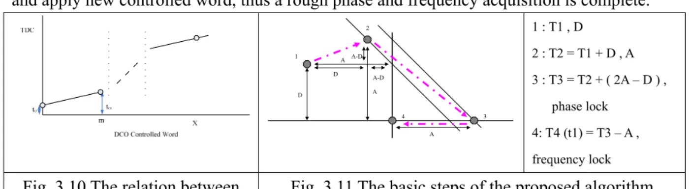
Initially, DCO set the minimum cycle time after power on. The controlled word in DCO would be zero. After the first edge of reference clock comes, the controlled word will be added by a constant value, P, at every positive edge of divided output clock. How to determine P depends on the ration of the scales between TDC and DCO. Selecting the value which can be detected the difference in TDC while the multiplication factor sets the minimum value is recommend. After the second edge of reference clock comes, the controlled word will be held and TDC gets the corresponding value. If we assume the DCO is linear, which is shown in Fig. 3.10, we can write the equation (3-4) from the relation of reference clock and divided output clock. In equation (3-4), k = tm-t0 / m, where t0 is the
TDC value of intrinsic delay time in DCO; tm is the TDC value when control word is m; and
X is corresponding controlled word value we want to calculate. We get the control word form equation (3-5) which rewrite from the equation (3-4).
k X + t 1)k) -(m + (t + … + 2k) + (t + 1k) + (t + 0k) + (t0 0 0 0 ≅ 0 (3-4) )) t -(m/(t )/2 t + 1)(t -(m X≅ m 0 ∗ m 0 (3-5)
When the calculation is complete, ADPLL will wait the coming of third positive edge and apply new controlled word, thus a rough phase and frequency acquisition is complete.
D A A D A-D A-D A 1 2 3 4 1 : T1 , D 2 : T2 = T1 + D , A 3 : T3 = T2 + ( 2A – D ) , phase lock 4: T4 (t1) = T3 – A , frequency lock
TDC and DCO control word
3.4.2. Coarse Tracking Algorithm
Fig. 3.11 illustrates the basic steps of the proposed algorithm, and its corresponding waveform is shown in Fig. 3.12. There are four fundamental cycles. The initial cycle time of divided output clock is T1 at 1, and we get the phase error, D, between the first and the second cycles. Then we update the DCO setting with T1 + D to form the T2, and get phase error A at 2. Because we want to create a phase lock at 3 and we know the oblique line always is in Fig. 3.11, we can calculate where the position 3 is by the property of the isosceles triangle. Finally, we get frequency lock at 4 by the same method.
o
45 −
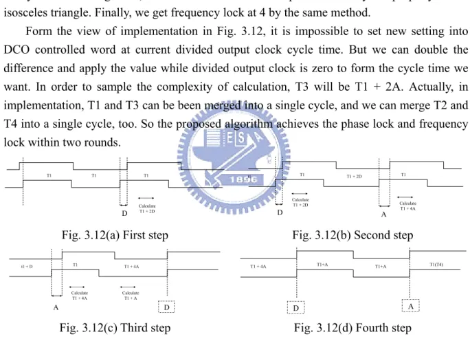
Form the view of implementation in Fig. 3.12, it is impossible to set new setting into DCO controlled word at current divided output clock cycle time. But we can double the difference and apply the value while divided output clock is zero to form the cycle time we want. In order to sample the complexity of calculation, T3 will be T1 + 2A. Actually, in implementation, T1 and T3 can be been merged into a single cycle, and we can merge T2 and T4 into a single cycle, too. So the proposed algorithm achieves the phase lock and frequency lock within two rounds.
D T1 T1 T1 Calculate T1 + 2D D T1 + 2D T1 t1 A Calculate T1 + 2D Calculate T1 + 4A T1
Fig. 3.12(a) First step Fig. 3.12(b) Second step
t1 + D A Calculate T1 + 4A T1 T1 + 4A Calculate T1 + A D T1 + 4A T1+A T1+A T1(T4) D A
Fig. 3.12(c) Third step Fig. 3.12(d) Fourth step
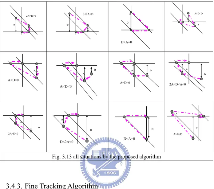
Fig. 3.13 illustrates the other situation by the proposed algorithm. Clearly, the proposed algorithm is robust at any position.
A>D=0 A A D A D A 0<D<A D A D A 0<D=A D A D A 2A>D>A>0
D A D A 2A=D>0 D A D A 0<2A<D D D D>A=0 D A D A A<0<D A A A<D=0 D A D A A<D<0 D A D A A=D<0 D A D A 2A<D<A<0 D A D A 2A=D<0 D A D A D<2A<0 D D D<A=0 D A D A A>0>D
Fig. 3.13 all situations by the proposed algorithm
3.4.3. Fine Tracking Algorithm
When the sensitivity of TDC is not enough to detect and the input jitter is very small, and we still have a little bits of DCO controlled word that TDC can not sense the difference between them, the ADPLL enters the fine tracking mode. The ADPLL add or subtract the controlled word with a gain register according to the direction which phase detector indicates. The initial value of the gain register is the corresponding value of one step time of TDC. Fig. 3.14(a) illustrates the behavior when the reference clock within the gain windows which rate is 1.2 : 1 from two points. Clearly, the average phase error will shift up if the average cycle time is smaller than reference clock, otherwise the average phase error will shift down if the average cycle time is bigger than reference clock. In the shift up case in Fig. 3.14(a), the direction will not change after the long running, and the gain register can be reduced to the half. If the reference clock locates on the center of gain, as show in Fig. 3.14(b), the average phase error will never change; so, we subtract the gain register by one.
1.2:1
Gain register value
Gain register value be the half
Phase lock
Reference clock
1:1
Gain register value
Gain register value Subtract by
one
Reference clock
Fig. 3.14(a) Fig. 3.14(b)
In order to maintain the position always locate on the quadrant (-, +) or quadrant (+, -), we need to handle the situation when the position locates on the quadrant (+, +) or (-, - ). The simplest way is to wait the changing of direction. In order to prevent that the ADPLL wait too long, we use the offset register and round register to tune the gain register. The initial value of offset register and round register is one, and we give it a chance when the first event that the direction does not change occurs; but the gain register is reduced and the round register is subtracted by one. If the direction still does not change, the gain register is added by the offset register to speed up the locking process. In order to prevent the offset register grow too quick, we define a rule, the bigger the offset register is, the more chance it has. So every time the offset register grows up, the round register grows up, too. When the round register become to zero, the offset can be been added by one. The more detail of flow chart is shown in Fig. 3.15.
3.5.
HDL Jitter Model
In order to increase the accuracy for ADPLL simulations, it is requisite to model jitter phenomena in HDL simulation environment. If this idea can be realized, the difference between simulations and measured results can be reduced. On the other hand, the accuracy of simulation is improved to approach real situations. For implementations, jitter needs to be handled carefully when locked stability takes into account. To compensate for jitter, DSP schemes are requisite to eliminate these imperfections. Generally, a portable design must be able to apply to different cell library by synthesis tool. Hence, it is necessary to model jitter before performing synthesis to a target cell library - a HDL jitter model must be established to verify possible ADPLL architectures.
For simplification without losing generality, we define a parameter, ∆ jitter, which is
modeled by triangular distribution. Fig. 3.16 illustrates the relation between input parameter p% and its waveform, where ∆ noise is modeled by uniform distribution and T is the period of
non-jitter signal or named the central frequency. The period of output clock is T jitter, where T
jitter = T + △ jitter. For example, the input parameter is 1%, and reference clock cycle time is
500 ns, the period of output clock with jitter is from 495 ns to 505 ns. The histogram is shown at left side.
a1 a2 a3 a4 a5 a6 a7 a8 a9 a10 b1 b2 b3 b4 b5 b6 b7 b8 b9 b10 b10 Max pulse = T/2 + p%*(T/2) + p%*(T/2) Min pulse = T/2 -p%*(T/2) - -p%*(T/2)
Min cycle time = T -p%*(T/2) - -p%*(T/2)
Max cycle time = T + p%*(T/2) + p%*(T/2) c i( ∆jitter ) : bi– bi-1 b i ( ∆noise) : - (T / 2) x p% ~ + (T / 2) x p% a i: cycle time / 2 = ( T / 2 ) Fig. 3.16
By this HDL jitter model, many real situations are easily monitored in computer simulations to help engineers improve their designed efficiency. From above descriptions, it has also provided that the HDL jitter model can be used to verify the performance of possible architectures in noise (jitter) environment. Hence, designers can improve their solutions to prevent and reduce careless problems, such as locked bandwidth, tracking performance, and circuit stability … etc.
3.6.
Jitter Reduction
3.6.1. Types of Jitter
There are many different types of jitter. Period jitter, cycle-to-cycle jitter and long-term jitter are described below.
Fig. 3.17 Period jitter Fig. 3.18 Cycle-to-cycle jitter Fig. 3.19 Long-term jitter (1) Period Jitter : Period jitter is the maximum change in a clock’s output transition from
its ideal position. Fig. 3.17 is a graphical representation of period jitter.
(2) Cycle-to-Cycle Jitter : Cycle-to-cycle jitter is the change in a clock’s output transition from its corresponding position in the previous cycle. Fig. 3.18 depicts the graphical representation of cycle-to-cycle jitter. J1 and J2 are the jitter values measured for single ended signals. The maximum of such values measured over multiple cycles is the maximum cycle- to-cycle jitter.
(3) Long-term Jitter : Long-term jitter measures the maximum change in a clock’s output transition from its ideal over a large number of cycles. Fig. 3.19 is a graphical representation of long-term jitter. The actual number of cycles depends on the application and the clock frequency. Long-term jitter is also called accumulated jitter.
3.6.2. Tradeoffs Between Loop Filter Parameters
From above descriptions, jitter must be eliminated to make output as clean as possible. With considerations of cost and performance, the mean processing is a useful scheme to reduce noise or jitter, which it can average the spectrum in frequency domain or period in time domain. By taking algorithm complexity into account, it is not flexible to average signals in frequency domain because it needs more procedures for Fourier transform and inverse transform. The period after mean processing (it is activated in time domain) is equal to n T T n jitter average
∑
= 1 = n T n jitter∑
Δ + 1 (3-6)Note that the second term in equation (3-6) can be regarded as a period error after mean processing. By central limit theorem (CLT), it is shown that the variance after mean processing in equation (3-6) is smaller than origin one. This means that the jitter has been decreased by applying mean value. Theoretically, it is impossible to completely remove jitter; however it can be reduced by large “n”. On the other hand, it is possible to minimize the period error in equation (3-6); however the error can not be eliminated. General speaking, the response time is also proportional to “n”, the number of average cycles. Because of physical limitations, such as size, complexity, and speed … etc, “n” can not be set too large in implementation. As a result, the average processing is a recycle action per “n” to trade off both period error and response time.
In order to reduce the cycle-to-cycle jitter and period jitter, IIR-like filter is added in ADPLL. The more degree the filter has, the more jitter be reduced. However the phase error and long-term jitter will be enlarged. The relation between the IIR filter degree and output jitter at 80MHz DCO output, under 2 MHz reference clock with HDL jitter model, where the peak-to-peak period jitter is ±5000ps, is shown in Fig. 3.20. From Fig. 3.20, IIR degree = 4 is a proper selection to trade off costs and performance.
Fig. 3.20(a) The peak-to-peak value of long-term jitter and phase error
Fig. 3.20(b) The rms value of long-term jitter and phase error
Fig. 3.20(c) The peak-to-peak value of period jitter and cycle-to-cycle jitter
Fig. 3.20(d) The RMS value of period jitter and cycle-to-cycle jitter
As a result, the filter of ADPLL needs to be programmable to achieve variable applications. The structure of filter is shown in Fig. 3.21, where the C is controlled word and the degree of IIR filter is four. Because the coarse algorithm get phase & frequency lock every two reference cycles, the mean processing works every two reference cycles. And the IIR-like filter works every DCO cycle.
C C new 1/4 3/4 R1 R2 1/8 1/8 1/2 n C n ∑ 1 Mux IIR R3 R4 1/8 1/8
Fig. 3.21 The structure of filter
3.7.
Simulation Results
In this section, we will discuss the simulation result with HDL jitter model. The environment is as follows. The control bit of the DCO is 23 bits. The finest resolution is 1.55ps and the intrinsic delay is about 1ns. The dead zone of phase detector is 50ps. The “n” is 128 for mean processing.
Fig. 3.22 illustrates the relation between jitter performance and multiplication factor. The reference clock is 10 KHz (100000ns); the peak-to-peak jitter of reference clock is ±1000ps. The DCO frequency is form 100 KHz to 10MHz. It is shown that the long-term jitter and phase error will increase when the multiplication factor increases; the absolute value of the period jitter and cycle-to-cycle jitter tend toward a constant value, but the relative value increase, too. The corresponding waveform when multiplication factor is 10 and 1000 are shown in Fig. 3.23 and Fig. 3.24.
Fig. 3.22(a) The average period of DCO vs. multiplication factor
Fig. 3.22(b) The peak-to-peak long-term jitter and peak-to-peak phase error vs.
multiplication factor
Fig. 3.22(c) The peak-to-peak period jitter and peak-to-peak cycle-to-cycle jitter vs.
multiplication factor
Fig. 3.22(c) The peak-to-peak period jitter and peak-to-peak cycle-to-cycle jitter (%
output period) vs. multiplication factor
Fig. 3.23 The waveforms and its close view when multiplication factor is 10
From behavior simulations at 80MHz DCO output, the period is 12.5ns, under 2 MHz reference clock, the period is 500ns, with HDL jitter model, where the ratio of peak-to-peak period jitter is from ± 0% to ± 1% of reference clock, the peak-to-peak value is form ±0ns to ±5ns. The relation between input jitter and output jitter is shown in Fig. 3.25. Clearly, the output jitter and phase error will increase when the input jitter increase. Because the phase error between idea clock and reference clock with jitter is never smaller than the input period jitter, and it is impossible to generate the idea clock, the value of “PkPk phase error” is never smaller than the value of input period jitter. Fig. 3.25(g) shows the histogram of output clock when the input peak-to-peak jitter is ± 1 %; the histogram of input clock is shown in Fig. 3.16. Fig. 3.26(h) shows the histogram of output clock when the input jitter is zero.
Fig. 3.25(a) The peak-to-peak value of long-term jitter and phase error vs. peak-to-peak input jitter from 0% to ±1 %
Fig. 3.25(b) The RMS value of long-term jitter and phase error vs. peak-to-peak input
jitter from 0% to ±1 %
Fig. 3.25(c) The peak-to-peak value of period jitter and cycle-to-cycle jitter vs. peak-to-peak input jitter from 0% to ±1 %
Fig. 3.25(d) The peak-to-peak value of period jitter and cycle-to-cycle jitter relate to output period vs. peak-to-peak input jitter
Fig. 3.25(e) The RMS value of period jitter and cycle-to-cycle jitter vs. peak-to-peak input jitter from 0% to ±1 %
Fig. 3.25(f) The RMS value of period jitter and cycle-to-cycle jitter vs. peak-to-peak
input jitter from 0% to ±1 %
Fig. 3.25(g) The histogram of output clock when input jitter is ±1%
Fig. 3.25(h) The histogram of output clock when input jitter is ±0%
From behavior simulations at 30.72MHz DCO output, the period is 32.5ns, under 30 KHz reference clock, the period is 33333.3ns, with HDL jitter model, where the ratio of peak-to-peak period jitter is from ± 0% to ± 1% of reference clock, the peak-to-peak value is form ±0ns to ±333.3ns. The relation between input jitter and output jitter is shown in Fig. 3.26. To compare with ISSCC04 [3], which list in Table 3.1, the proposed algorithm get the same jitter performance under ± 0.55% of input jitter from our simulation result. That means the proposed algorithm will get the better performance when the real input jitter is smaller than ±183.3ns.
Fig. 3.26(a) The peak-to-peak value of period jitter and cycle jitter vs. peak-to-peak
input jitter from 0% to ±1 %
Fig. 3.26(b) The peak-to-peak value of period jitter and cycle jitter vs. peak-to-peak input jitter from 0% to ±1 %
Fig. 3.26(c) The RMS value of period jitter and cycle jitter vs. peak-to-peak input jitter
from 0% to ±1 %
Fig. 3.26(d) The RMS value of period jitter and cycle jitter vs. peak-to-peak
input jitter from 0% to ±1 %
Performance Parameter This work ISSCC’04[3]
Process simulation under 90nm CMOS 90nm CMOS
Approach TDC + single DCO PFD + TDC Digital loop
Input Range Min. cycle time :
max { TDC delay line + 2 x ( Register x 2 + ALU ) + filter + 2 x Register + DCO decoder, N x ( intrinsic delay of DCO ) x 20 }
Max. cycle time :
4 x { max. DCO clock cycle time }, (while TDC register doesn’t overflow)
30 KHz ~65 MHz
Output Range Depend on process and the bit numbers of DCO controlled word
0.18~600 M
Multiplication Factor 4 ~ the bit numbers of divider 1 ~ 1023 Max. Lock time Theoretical cycle : 4 after power on >150
Output Jitter (peak-to-peak) ±0.6 % @ 30.72MHz, N=1024 ±0.6 % @ 30.7 MHz, N=1023
input jitter (peak-to-peak) ±183.3ns (±0.55 % ) @ 30 KHz Unknown @ 30 KHz Table 3.1 To compares with different PLL
Chapter 4
The proposed ADPLL Architecture
4.1.
ADPLL Architecture Overview
Based on the algorithm proposed in chapter 3, the corresponding architecture of TDC based ADPLL is shown in Fig. 4.1. There are ten basic modules; frequency error detector, flag, delay time selector, estimator, register files, arithmetic logic unit, DCO, DCO controlled word buffer, ADPLL controller, frequency divider. The details of each module will be illustrated at next section.
TDC Estimator Instruction Control DCO Frequency Divider Reference clock HSPD Decoder ALU Divider Adder Register N M u x DTS DFF Multiplier FED FLAG addr Reg ist e r Update Register Decoder Filter InstBuf DCWB DCO clock Divided output clock
Fig. 4.1 The proposed architecture
4.2.
Circuit Designs
4.2.1. Digital-Controlled Oscillator (DCO)
A high-resolution cell-based DCO is shown in Fig. 4.2, which includes two or three major parts depend on application. One is fine module to provide the high resolution; the other is coarse module to provide the wide clock range; the last is the heavy module to provide the ultra wide range that the coarse module can’t support. The heavy module is optional depend on which application.
. . . MUX 1'b1 Mask[0] 1'b1 Mask[n/2-2] 1'b1 Coarse module Delay chain Counter = M U X DFF Heavy module Controlled word Controlled word Fine mudle Reset
Fig. 4.2 The proposed DCO
The basic idea of heavy module is a delay loop, which equal the maximum delay time of whole DCO loop. The goal of this module is to save the delay line in coarse module.
The coarse module uses the NAND gate delay chain to replace the inverter gate delay chain. When the total intrinsic delay time is small than the delay time at inverter delay chain, it will cause function error if controlled word switch from the lowest to the highest; it is shown in Fig. 4.3. Because this reason, we use the NAND gate as our coarse module. And we get efficiency of the stable DCO and power saving also. But if the intrinsic delay time is bigger than the delay time at inverter, the inverter delay version is recommended.
The fine module uses novel varactors, which is proposed in [4]. The proposed DCO get high resolution with the fine module, and has ability of wide bandwidth generation with the heavy module.
Fig. 4.3 The problem of inverter delay line
As discussion in chapter 2, the structure of TDC is shown in Fig. 2.5. Actually, the trouble in TDC design is the synchronism between latches in the delay line and the counter. It is needed a method to prevent the wrong when the delay line finish a count but the input turn off and counter had not added by one. The propose TDC uses a flag register to detect and choose the correct value.
4.2.3. HSPD with Pulse Amplifier
The HSPD was proposed in [5]. We choose the HSPD with modification as our phase detector. In order to prevent the width violation, the proposed pulse amplifier to modify the pulse width to meet the circuit requirement. The proposed pulse amplifier is shown in Fig. 4.4. And the corresponding waveform is shown in Fig. 4.5. Be careful the TAND must be less than
TOR. TDelay TAND TOR IN OUT
TOUT-MIN = T Delay + TAND + TOR
If TOR < TIN < TOUT-MIN
TOUT = TOUT-MIN
If TOUT-MIN < TIN
TOUT = TIN
Fig. 4.4 The proposed pulse amplifier
TIN
TOR TAND T
Delay TAND TOR
TOUT
Fig. 4.5 The corresponding waveform of proposed pulse amplifier
4.2.4. Frequency Error Detector (FED)
In order to prevent tracking fail of DCO due to the violent change of reference clock, the ALPLL uses a “watching dog” to monitor reference frequency and divided output frequency
during phase tracking. The basic idea of frequency error detector is shown in Fig. 4.6(a). The behavior of frequency error detector is like an up-down counter. Fig. 4.6(b) is the proposed structure to realize; where the “Pos Pulse” output a pulse when input positive edge of clock, the “Neg Pulse” output a pulse when input negative edge of clock.
DFF DFF Pos Pulse Neg Pulse DFF DFF 1'b1 1'b1 clk clk clk reset reset set set set set Reference clock Divided output clock Reset Error
Fig. 4.6(a) The behavior of frequency error detector
Fig. 4.6(b) The structure of frequency error detector
4.2.5. Flag
The goal of flag is to notify the DTS the current state of ADPLL, including the frequency error or not, the value of TDC is zero or not … etc.
4.2.6. ALU
In order to save the gate count and reduce the complexity of ADPLL, the proposed ADPLL share the arithmetic logic unit in the different time. There are two adders, two multipliers and one divider.
4.2.7. Register
Although the proposed ADPLL is general purpose-like design, the register file has different size of registers in order to reduce the redundant logic.
4.2.8. Delay Time Selector
The basic idea of delay time selector is a similar to DCO. There are four paths to select according the delay time which the current instruction needs. For example, if current instruction is to divide or to multiply in ALU, the DTS select the longest path; if the current
instruction is just a jump to another address, and the DTS select the shortest path. The other function DTS supported is to point out the address of current instruction and determine the next address according to the flag output. The proposed structure is shown in Fig. 4.7.
Fig. 4.7 The proposed structure of delay time selector
4.2.9. Controller
The controller has two basic sub modules, one defines the instruction flow, and the other defines the controlled signals for each module in ADPLL. According to the address DTS provided, the controller generates the correct controlled signals.
4.2.10.
DCO Controlled Word Buffer (DCWB)
The DCO controlled word buffer is a buffer between whole controller with the internal clock and DCO loop with the DCO clock. There are four sub modules, instBuf is used to hold the average controlled word after mean-process and hold the current controlled word; the Filter is used to smooth the controlled word which is discussed in section 3.6.2; the decoder is used to decode the controlled word; and the update register update the decode values at correct time.
4.2.11.
Frequency Divider
Frequency divider is used to divide the DCO clock. Because the proposed coarse algorithm works on the situation when the multiplication factor is even number, we need to divide the input reference clock when the multiplication factor is odd number. Because of dividing by two of reference clock and divided output clock simultaneously has the same DCO output clock, the ADPLL still works very well.
Chapter 5
Conclusion and Future Work
5.1.
Conclusion
In order to realize All-Digital PLL, new approaches have been presented to offer portable, full-integration and low-jitter frequency synthesizer in digital VLSI. The phase state
diagram is proposed to analyze the relation between phase and frequency; the new phase tracking & frequency search algorithm is proposed to achieve fast phase and frequency lock; the proposed ADPLL with single DCO solves the mismatch problem in clock pair
architecture; A DSP based architecture is proposed to provide a programmable and stable ADPLL; By cell-based digital approach, it provides ADPLL with capability of fully pulling bandwidth. For improving simulation, a HDL jitter model is completed to help designs more efficient and accurate in noisy environment. As a result, the proposed ADPLL is very
suitable for variable application as demanded in current SoC designs.
5.2.
Future Work
The following topics to extend the work can be proposed.
(1) To provide a power-saving mode for low-power or mobile applications, so the system can turn off the ADPLL if needed.
(2) To enhance the resolution of DCO. Digitally controlled oscillator is the key component of all-digital PLL. It is very hard to design a cell-based DCO with good linearity and small area. But we will have a precise clock if we have a precise DCO.
(3) To design an all-digital multi-phase locked loop based proposed ADPLL with modification. Multi-phase clocks are useful in many applications such as high speed serial link.
(4) The proposed algorithm can be implemented with DSP for programmable and portable issue
References
[1] Terng-Yin Hsu, chung-Cheng Wang, and Chen-Yi Lee, “Design and analysis of a Portable High-Speed Clock Generator,” IEEE Transactions on Circuit and Systems II: Analog and Digital signal Processing, vol. 48, pp. 367-375, Apr. 2001
[2] J. Dunning, G. Garcia, J. Lundberg, and Ed Nuckolls,”An All-digital Phase-Locked Loop with 50-cycle Lock Time Suitable for High Performance Microprocessors,” IEEE Journal of Solid-State Circuits, Vol. 30, No. 4, pp. 412-422, Apr. 1995
[3] J. Lin, B. Haroun, T. Foo, J.-S. Wang, b. Helmick, S. Randall, T. Mayhugh, C. Barr and J. Kirkpartick, “A PVT Tolerant 0.18 MHz to 600 MHz Self-Calibrated Digital PLL in 90 nm CMOS Process, “ in Dig. Tech. Papers ISSCC’04, Feb. 2004, pp. 488-489.
[4] Pao-Lung Chen, Ching-Che Chung and Chen-Yi Lee, “A Portable Digitally-Controlled
Oscillator Using Novel Varactors”, IEEE Trans. Circuits an Syst. II, Express brefs, Vol. 52,
No.5, pp.233-237, May 2005
[5] Ching-Che Chung and Chen-Yi Lee, “An all-digital phase-locked loop for high-speed clock generation,” IEEE Journal of Solid-State Circuits, Vol.38, pp. 374-351, Feb. 2003