Research Article
Efficiency and Droop Improvement in GaN-Based
High-Voltage Flip Chip LEDs
Yen-Chih Chiang,
1Bing-Cheng Lin,
2Kuo-Ju Chen,
2Sheng-Huan Chiu,
2Chien-Chung Lin,
3Po-Tsung Lee,
2Min-Hsiung Shih,
4and Hao-Chung Kuo
21Institute of Lighting and Energy Photonics, National Chiao Tung University, Tainan 71550, Taiwan
2Department of Photonics and Institute of Electro-Optical Engineering, National Chiao Tung University, Hsinchu 30010, Taiwan
3Institute of Photonics System, National Chiao Tung University, Tainan 71550, Taiwan
4Research Center for Applied Sciences, Academia Sinica, 128 Academia Road, Sec. 2 Nankang, Taipei 115, Taiwan
Correspondence should be addressed to Chien-Chung Lin; [email protected] and Hao-Chung Kuo; [email protected]
Received 13 February 2014; Accepted 2 June 2014; Published 30 June 2014 Academic Editor: Nelson Tansu
Copyright © 2014 Yen-Chih Chiang et al. This is an open access article distributed under the Creative Commons Attribution License, which permits unrestricted use, distribution, and reproduction in any medium, provided the original work is properly cited.
The GaN-based high-voltage flip chip light-emitting diode (HVFC-LED) is designed and developed for the purpose of efficiency enhancement. In our design, the distributed Bragg reflector (DBR) is deposited at the bonded substrate to increase the light extraction. After the flip chip process, the general current-voltage characteristics between the flip chip sample and the traditional sample are essentially the same. With the help of great thermal conductive silicon substrate and the bottom DBR, the HVFC-LED is able to enhance the power by 37.1% when compared to the traditional high-voltage LEDs. The wall-plug efficiencies of the HVFC-LED also show good droop reduction as high as 9.9% compared to the traditional devices.
1. Introduction
The availability of high brightness, high power, and large area of GaN-based light-emitting diodes (LEDs) has enabled their applications in exterior automotive lightings, outdoor displays, backlights for liquid crystal display (LCD) TVs, var-ious handheld devices, printers, and rear projection TVs [1]. However, the notorious efficiency droop phenomenon makes the GaN LEDs more power-consuming at higher current and causes the increase of chip cost. Various mechanisms have been proposed as the reasons of this efficiency droop, including electron leakage out of the active region, Auger recombination, carrier delocalization, and poor hole injec-tion [2–5]. To further reduce the production cost and enhance the performance of these LEDs, there is always a great need to improve the external quantum efficiency (EQE) and solve the efficiency droop. Recent studies have substantially alleviated droop by new active region design such as reduced charge separation [6–8], nano/microphotonics structures [9, 10], novel growth and substrate technologies [11], and barrier
engineering [12]. In addition, the optimization of the light extraction efficiency is of great importance to achieve large EQE in the nitride-based LEDs. Previously, it has been shown that one can utilize a transparent contact layer (TCL) [13], patterned sapphire substrates (PSSs) [14, 15], surface texturing (ST) [16], and/or flip chip (FC) technology [17– 19] to enhance light extraction of nitride-based LEDs. Using TCL, one can reduce absorption of the conventional Ni-Au 𝑝-contact layer. One can reduce dislocation density in the epitaxial layers and also enhance light scattering at GaN— sapphire interface by PSS technology. With ST technology, photon emission can be randomized by surface scattering due to the roughened top surface of the LED. By FC technology, one can achieve larger LED output power since no bonding pads or wires exist on top of the devices so that photons could be emitted freely from the substrates.
Until recently, the traditional sapphire-based high power LED still dominates the lighting market. Due to poor thermal conductivity of the sapphire substrate, high operational cur-rent leads to curcur-rent-crowding and bad thermal dispersion
Volume 2014, Article ID 385257, 7 pages http://dx.doi.org/10.1155/2014/385257
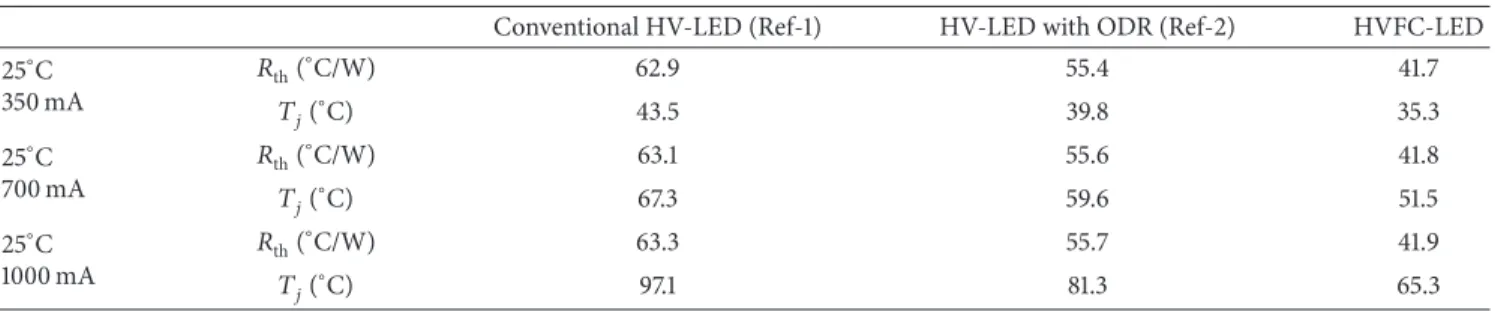
Table 1: The Rthand𝑇𝑗comparison of three kinds of LED.
Conventional HV-LED (Ref-1) HV-LED with ODR (Ref-2) HVFC-LED
25∘C 350 mA 𝑅th(∘C/W) 62.9 55.4 41.7 𝑇𝑗(∘C) 43.5 39.8 35.3 25∘C 700 mA 𝑅th(∘C/W) 63.1 55.6 41.8 𝑇𝑗(∘C) 67.3 59.6 51.5 25∘C 1000 mA 𝑅th(∘C/W) 63.3 55.7 41.9 𝑇𝑗(∘C) 97.1 81.3 65.3
problem. These problems are always haunting the high-current performance of the traditional LEDs. Recent research on high-voltage light-emitting diode (HV-LED) has shown that multiple series-connected microdiodes in a single large chip can obtain high forward voltage with a low driving cur-rent, thereby reducing current crowing and efficiency droop [20–22]. Moreover, the HV-LED can effectively avoid thermal problem due to relatively low operating current. Another advantage brought by high-voltage/low current operation is the direct utilization of the regular wall plug outlet without further voltage conversion. These features, combined with fewer wire-bonding needed, make HV-LED attractive for commercial applications.
In this study, a high-voltage flip chip LED (HVFC-LED) which consists of𝑛-side up multiple series-connected diodes is demonstrated. This design provides high thermal conductivity and high bottom reflection silicon submount. In addition to these features, a high wall-plug efficiency can be expected [22]. In the subsequent text, we will discuss fabrications and performance analysis of this device.
2. Device Fabrication and Measurement
In the experiment, the LEDs were grown on 𝑐-plane sap-phire substrate by metal-organic chemical vapor deposition (MOCVD) system. The structure includes a 𝑛-GaN layer, an In𝑥Ga1−𝑥N/GaN multiple-quantum wells, a 𝑝-AlGaN electron blocking layer, and a𝑝-GaN layer. In the device fab-rication, firstly, a 120 nm indium tin oxide (ITO) transparent conductive layer was deposited by e-beam evaporator. Then, the mesa of microchips and𝑛-contact area were etched by inductively coupled plasma (ICP) etcher. After that, the 10𝜇m trenches were etched by ICP between microchips [22–24]. To prevent the short circuit between each microchip, the passiva-tion SiO2layer (700 nm) was deposited by plasma enhanced chemical vapor deposition (PECVD), and the interconnected Cr/Pt/Au (50/50/1500 nm) was up to evaporation by e-beam evaporator to serve as cathodes. Until this step, the multiple series-connected diodes are done.
Before connecting the chip and the submount, 15 pairs of SiO2/TiO2distributed Bragg reflector (DBR) were prepared on silicon submount by e-beam evaporator [25]. Finally,
through 280∘C 15 min thermal reflow, the 45 mil× 45 mil chip is flip mounted on this reflective silicon submount by gold-tin eutectic bonding and then the process is finished. For comparison purpose, two different types of packaged LED chips were prepared: the first one is the conventional HV-LED with patterned sapphire substrate and the other is similar to HV-LED but extra 5.5 pairs of SiO2/TiO2 and Al/Ti/Ni/Au omnidirectional reflector (ODR) layer were deposited at the bottom of sapphire substrate. Both types of devices are of the same chip size and referred to as HV-LED and HV-LED + ODR, respectively.
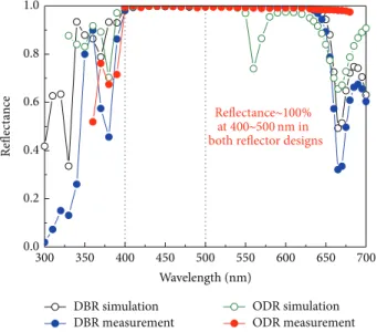
Figure 1shows the schematic diagrams of the three LEDs [26]. To have a fair comparison, the reflectivities at 455 nm for both DBR and ODR were close to 100%. Both reflectances were shown inFigure 2. The optical and electrical characteris-tics of the devices were measured at room temperature using a manual probing system with integrating sphere detector and supplying steady DC current by Keithly 2600 [27]. In order to eliminate the thermal effect under continuous DC current which can decimate to lead the light output power, a separate 𝐿-𝐼-𝑉 characteristic under pulse mode with 2.5% duty cycle was performed.
Thermal dispersion of substrate can be analyzed by using T3Ster thermal transient tester to measure thermal resistance (𝑅th) and junction temperature (𝑇𝑗). FromTable 1, the HVFC-LED clearly has a leading edge on both𝑅thand𝑇𝑗. These data strengthen the claim that HVFC-LED has good thermal dispersion.
3. Results and Discussion
Figure 3shows the𝐿-𝐼-𝑉 curves of these three LED devices. At the same 20 mA driving current, the forward voltages of these three LEDs were 49.0∼50.0 V. Compared with con-ventional HV-LED and HV-LED + ODR, the light output power of HVFC-LED is found to be enhanced by 37.1% and 5.1% at the same 20 mA current injection, respectively. There are two main reasons for the large enhancement of power intensity: The configuration of HVFC-LED provides better thermal conductivity by extra high reflection and high thermal conductive silicon submount (silicon∼120 W/mK
MQWs
N-GaN
Pattern sapphire substrate Interconnection Passivation Interpassivation P P N N TCL N-GaN P-GaN P-GaN (a)
Pattern sapphire substrate TCL P P N N Passivation Interconnection MQWs ODR N-GaN N-GaN P-GaN P-GaN (b) TCL P P N N MQWs Passivation DBR Interconnection Submount Gold-tin eutectic N-GaN N-GaN P-GaN P-GaN
Pattern sapphire substrate
n = 2.45 n = 1.8
(c)
Figure 1: Schematic diagrams of (a) the conventional HV-LED, (b) HV-LED + ODR, and (c) high-voltage flip chip LED (HVFC-LED).
300 350 400 450 500 550 600 650 700 0.0 0.2 0.4 0.6 0.8 1.0 Refle ct an ce Wavelength (nm) DBR simulation DBR measurement ODR simulation ODR measurement Reflectance∼100% at 400∼500 nm in
both reflector designs
Figure 2: The reflectance in measurement results and simulation data between distributed Bragg reflector (DBR) and omnidirectional reflector (ODR).
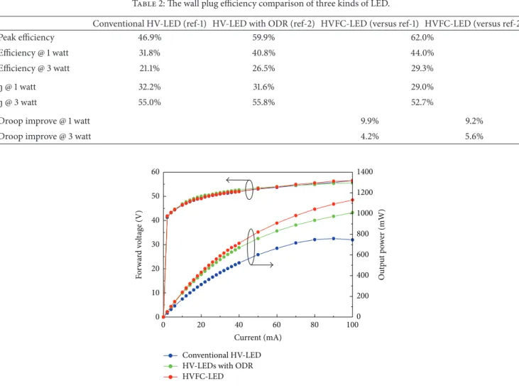
Table 2: The wall plug efficiency comparison of three kinds of LED.
Conventional HV-LED (ref-1) HV-LED with ODR (ref-2) HVFC-LED (versus ref-1) HVFC-LED (versus ref-2)
Peak efficiency 46.9% 59.9% 62.0%
Efficiency @ 1 watt 31.8% 40.8% 44.0%
Efficiency @ 3 watt 21.1% 26.5% 29.3%
p @ 1 watt 32.2% 31.6% 29.0%
p @ 3 watt 55.0% 55.8% 52.7%
Droop improve @ 1 watt 9.9% 9.2%
Droop improve @ 3 watt 4.2% 5.6%
0 20 40 60 80 100 0 10 20 30 40 50 60 Current (mA) Conventional HV-LED HV-LEDs with ODR HVFC-LED 0 200 400 600 800 1000 1200 1400 Ou tp u t p o w er (mW) F o rw ar d v o lt ag e ( V )
Figure 3: Forward voltage and light output power as a function of current for the three LEDs under pulse current injection.
versus Al2O3 ∼ 25 W/mK) and not any effect by electrode shadow, thus leading to higher light output power and better efficiency.
Due to different packaging design, even though the reflectances of ODR and DBR are similar, the outcomes are different. In the HV-LED + ODR design, the outgoing photons have to travel through a thick𝑛-type GaN and a thick sapphire substrate before hitting the ODR layer structure. This trip through𝑛-GaN can effectively reduce the reflected photons by the extra scattering and GaN absorption, and thus the effect of ODR is hindered. On the contrary, in the flip chip bonded device the photons travel much less distance before reaching the DBR layer, and the bouncing of the photons can be more pronounced than HV-LED + ODR case.
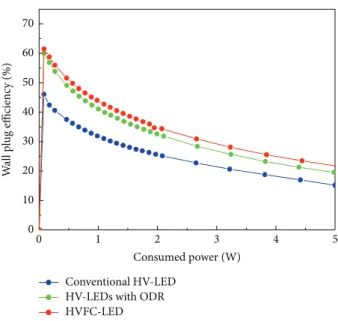
All these factors can be seen via the output powers and efficiencies shown in Figures3and4. The device efficiencies of the conventional HV-LED, HV-LED + ODR, and HVFC-LED at the same 1 watt consumed power were calculated as 31.8%, 40.8%, and 44.0%, respectively. The device efficiency droop can be written as
droop= (1 − 𝜂high current
𝜂max ) × 100%. (1)
According to (1), the droops of the conventional HV-LED, HV-LED + ODR, and HVFC-LED were calculated as 32.2%, 31.6%, and 29.0%, respectively (Table 2). As a result, the HVFC-LED possesses droop reduction of 9.9% and 9.2% in regard to traditional HV-LED and HV-LED+ODR. At 3 watts consumed power, thedroops of these three devices were calculated as 55.0%, 55.8%, and 52.7%, respectively. The HVFC-LED also improved efficiency droop 4.2% and 5.6% in regard to the other two devices. The major impact comes from the configuration of HVFC-LED which provides better thermal conductivity and photon extraction via silicon substrate and DBR deposition.
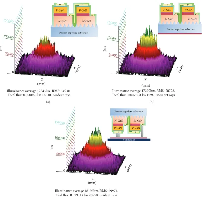
Figure 5shows the measured light pattern of these three LEDs. The light intensity distribution of these three kinds of devices was under the same measurement setting. The power intensity of HVFC-LED and two references were demonstrated in𝐿-𝐼-𝑉 curve, and the measured values were 432 mW, 411 mW, and 315 mW, respectively.Figure 6 shows the simulated results of these three LED devices by using the optical ray tracing simulation software. The model was composed of 15 units of LEDs with either top or bottom surface emission capabilities, and the emitted rays could
0 1 2 3 4 5 0 10 20 30 40 50 60 70 W al l p lug efficienc y (%) Consumed power (W) Conventional HV-LED
HV-LEDs with ODR HVFC-LED
Figure 4: The wall plug efficiency curves of these three LEDs at the same consumed power.
(a) (b) (c)
Figure 5: Light intensity distribution map of (a) the conventional HV-LED, (b) HV-LED + ODR, and (c) HVFC-LED.
escape the chip from either surfaces. As we discussed before, three cases were analyzed: (1) the rays directed through the sapphire substrate without any reflector as conventional HV-LED, (2) the rays reflected by reflector on the backside of sapphire as HV-LED + ODR device, and (3) the rays reflected by reflector of submount substrate as HVFC-LED model. As shown in simulation results, the total flux of conventional HV-LED, HV-LED + ODR, and HVFC-LED was approxi-mated 0.0200 lm, 0.0276 lm, and 0.0291 lm, respectively. The enhancement by the HVFC-LED compared to HV-LED and HV-LED + ODR cases is calculated as 45.5% and 5.4%. These values show good agreement with the enhancement of power intensity (37.1% and 5.1%) in experiment data. However, the calculation does not take into account the effects like current spreading or nonideal interface scattering which could erode the actual light extraction enhancement of our HVFC-LED
devices. This result confirms that the HVFC-LED design did contribute to increasing flux and power intensity.
4. Conclusion
In conclusion, the high-voltage flip chip light-emitting diodes (HVFC-LED) were investigated, and three types of devices including InGaN HVFC-LED, conventional HV-LED, and HV-LED + ODR were all prepared and tested at the same time. The results indicated HVFC-LED improved the power intensity around 37.1% and 5.1% compared to the other two types of devices under 20 mA drive. At the same time, the efficiency droop of HVFC-LED improved approximation to 9.9% and 9.2% compared to both references. When the consumed power is increased, the droop improvement is not scaled. These measurement and simulation results all point
X Y Lu x (mm) 0 50000 100000 150000
Illuminance average12543lux, RMS: 14930,
0.02006
Total flux: 8 lm 14840 incident rays
N-GaN
Pattern sapphire substrate
P P N N N-GaN P-GaN P-GaN (mm) (a) X Y Lu x (mm) 0 50000 100000 150000
Illuminance average17292lux, RMS: 20726,
Total flux:0.027668 lm 17985 incident rays
Pattern sapphire substrate
P P N N N-GaN N-GaN P-GaN P-GaN (mm) (b) X Y Lu x (mm) 0 50000 100000 150000
Illuminance average18199lux, RMS: 19971,
Total flux:0.029119 lm 28558 incident rays
P P
N
Submount
N-GaN N-GaN
P-GaN P-GaN Pattern sapphire substrate
N
(mm)
(c)
Figure 6: Simulated results of (a) the conventional HV-LED, (b) HV-LED + ODR, and (c) HVFC-LED.
out to the HVFC-LED being indeed a better design in terms of packaging, and we believe this design can be beneficial for the future generation of solid state lighting.
Conflict of Interests
The authors declare that there is no conflict of interests regarding the publication of this paper.
Acknowledgment
This work was supported in part by the National Science Council in Taiwan under Grant nos. NSC-103-3113-E-009-001-CC2 and NSC101-2221-E-009-046-MY3.
References
[1] S. Nakamura, T. Mukai, and M. Senoh, “Candela-class high-brightness InGaN/AlGaN double-heterostructure blue-light-emitting diodes,” Applied Physics Letters, vol. 64, no. 13, pp. 1687–1689, 1994.
[2] K. J. Vampola, M. Iza, S. Keller, S. P. DenBaars, and S. Nakamura, “Measurement of electron overflow in 450 nm InGaN light-emitting diode structures,” Applied Physics Letters, vol. 94, no. 6, Article ID 061116, 2009.
[3] C. H. Wang, J. R. Chen, C. H. Chiu et al., “Temperature-dependent electroluminescence efficiency in blue InGaN–GaN light-emitting diodes with different well widths,” IEEE Photonics Technology Letters, vol. 22, no. 4, pp. 236–238, 2010.
[4] A. David and M. J. Grundmann, “Droop in InGaN light-emitting diodes: a differential carrier lifetime analysis,” Applied Physics Letters, vol. 96, no. 10, Article ID 103504, 2010.
[5] B. Monemar and B. E. Sernelius, “Defect related issues in the “current roll-off ” in InGaN based light emitting diodes,” Applied Physics Letters, vol. 91, no. 18, Article ID 181103, 2007.
[6] H. Zhao, G. Liu, J. Zhang, J. D. Poplawsky, V. Dierolf, and N. Tansu, “Approaches for high internal quantum efficiency green InGaN light-emitting diodes with large overlap quantum wells,” Optics Express, vol. 19, no. 14, pp. A991–A1007, 2011.
[7] H. Zhao and N. Tansu, “Optical gain characteristics of staggered InGaN quantum wells lasers,” Journal of Applied Physics, vol. 107, no. 11, Article ID 113110, 2010.
[8] J. Zhang and N. Tansu, “Improvement in spontaneous emission rates for InGaN quantum wells on ternary InGaN substrate for light-emitting diodes,” Journal of Applied Physics, vol. 110, no. 11, Article ID 113110, 2011.
[9] E. Rangel, E. Matioli, Y. S. Choi, C. Weisbuch, J. S. Speck, and E. L. Hu, “Directionality control through selective excitation of low-order guided modes in thin-film InGaN photonic crystal light-emitting diodes,” Applied Physics Letters, vol. 99, Article ID 171106, pp. 081104-1–081104-3, 2011.
[10] X. Li, R. Song, Y. Ee, P. Kumnorkaew, J. F. Gilchrist, and N. Tansu, “Light extraction efficiency and radiation patterns of III-nitride light-emitting diodes with colloidal microlens arrays with various aspect ratios,” IEEE Photonics Journal, vol. 3, no. 3, pp. 489–499, 2011.
[11] Y. J. Lee, C. H. Chiu, C. C. Ke et al., “Study of the excitation power dependent internal quantum efficiency in InGaN/GaN LEDs grown on patterned sapphire substrate,” IEEE Journal on Selected Topics in Quantum Electronics, vol. 15, no. 4, pp. 1137– 1143, 2009.
[12] H. Zhao, G. Liu, R. A. Arif, and N. Tansu, “Current injection efficiency induced efficiency-droop in InGaN quantum well light-emitting diodes,” Solid-State Electronics, vol. 54, no. 10, pp. 1119–1124, 2010.
[13] S. J. Chang, C. S. Chang, Y. K. Su et al., “Highly reliable nitride-based LEDs with SPS+ITO upper contacts,” IEEE Journal of Quantum Electronics, vol. 39, no. 11, pp. 1439–1443, 2003. [14] K. Tadatomo, H. Okagawa, T. Tsunekawa et al., “High output
power InGaN ultraviolet light-emitting diodes fabricated on patterned substrates using metalorganic vapor phase epitaxy,” Physica Status Solidi (A), vol. 188, no. 1, pp. 121–125, 2001. [15] Y. J. Lee, J. M. Hwang, T. C. Hsu et al., “Enhancing the output
power of GaN-based LEDs grown on wet-etched patterned sapphire substrates,” IEEE Photonics Technology Letters, vol. 18, no. 10, pp. 1152–1154, 2006.
[16] T. Fujii, Y. Gao, R. Sharma, E. L. Hu, S. P. DenBaars, and S. Nakamura, “Increase in the extraction efficiency of GaN-based light-emitting diodes via surface roughening,” Applied Physics Letters, vol. 84, no. 6, pp. 855–857, 2004.
[17] J. Lee, S. Na, J. Jeong et al., “Low resistance and high reflectance Pt/Rh contacts to p-Type GaN for Ga N-based flip chip light-emitting diodes,” Journal of the Electrochemical Society, vol. 152, no. 1, pp. G92–G94, 2005.
[18] S. J. Chang, W. S. Chen, Y. C. Lin et al., “Nitride-based flip-chip LEDs with transparent ohmic contacts and reflective mirrors,” IEEE Transactions on Advanced Packaging, vol. 29, no. 3, pp. 403–408, 2006.
[19] C. F. Shen, S. J. Chang, W. S. Chen, T. K. Ko, C. T. Kuo, and S. C. Shei, “Nitride-based high-power flip-chip LED with double-side patterned sapphire substrate,” IEEE Photonics Technology Letters, vol. 19, no. 10, pp. 780–782, 2007.
[20] K. Chen, H. Kuo, Y. Chiang et al., “Efficiency and droop improvement in hybrid warm white LEDs using InGaN and
AlGaInP high-voltage LEDs,” IEEE/OSA Journal of Display Technology, vol. 9, no. 4, pp. 280–284, 2013.
[21] K. J. Chen, H. T. Kuo, H. C. Chen et al., “High thermal stability of correlated color temperature using current compensation in hybrid warm white high-voltage LEDs,” Optics Express, vol. 21, article S2, pp. A201–A207, 2013.
[22] C. H. Wang, D. W. Lin, C. Y. Lee et al., “Efficiency and droop improvement in GaN-based high-voltage light-emitting diodes,” IEEE Electron Device Letters, vol. 32, no. 8, pp. 1098– 1100, 2011.
[23] Y. Ding, W. Guo, Y. Zhu, Y. Liu, J. Liu, and W. Yan, “Fabrication of high-voltage light emitting diodes with a deep isolation groove structure,” Journal of Semiconductors, vol. 33, no. 9, Article ID 094007, 2012.
[24] J. M. Hong, X. Y. Li, and P. J. Niu, “Review of recent HV-LED technology,” Applied Mechanics and Materials, vol. 220–223, pp. 2075–2078, 2012.
[25] S. J. Chang, C. F. Shen, M. H. Hsieh et al., “Nitride-based LEDs
with a hybrid Al mirror +TiO2/ SiO2DBR backside reflector,”
Journal of Lightwave Technology, vol. 26, no. 17, pp. 3131–3136, 2008.
[26] Y. P. Hsu, S. J. Chang, Y. K. Su et al., “InGaN/GaN light-emitting diodes with a reflector at the backside of sapphire substrates,” Journal of Electronic Materials, vol. 32, no. 5, pp. 403–406, 2003. [27] W. L. Guo, W. W. Yan, Y. X. Zhu et al., “Analysis on elec-trical characteristics of high-voltage GaN-based light-emitting diodes,” Chinese Physics B, vol. 21, no. 12, Article ID 127201, 2012.
Submit your manuscripts at
http://www.hindawi.com
Hindawi Publishing Corporation
http://www.hindawi.com Volume 2014 Inorganic Chemistry International Journal of
http://www.hindawi.com Volume 2014
Hindawi Publishing Corporation
http://www.hindawi.com Volume 2014
Carbohydrate
Chemistry
International Journal ofHindawi Publishing Corporation
http://www.hindawi.com Volume 2014 Journal of
Chemistry
http://www.hindawi.com Volume 2014
Hindawi Publishing Corporation http://www.hindawi.com Analytical Methods in Chemistry Journal of Volume 2014 Bioinorganic Chemistry and Applications Hindawi Publishing Corporation
http://www.hindawi.com Volume 2014
Spectroscopy
International Journal ofHindawi Publishing Corporation
http://www.hindawi.com Volume 2014
The Scientific
World Journal
Hindawi Publishing Corporation
http://www.hindawi.com Volume 2014
http://www.hindawi.com Volume 2014
Chromatography Research International Hindawi Publishing Corporation
http://www.hindawi.com Volume 2014
Applied ChemistryJournal of
Hindawi Publishing Corporation
http://www.hindawi.com Volume 2014
Hindawi Publishing Corporation
http://www.hindawi.com Volume 2014 Theoretical Chemistry Journal of
Hindawi Publishing Corporation
http://www.hindawi.com Volume 2014
Journal of
Spectroscopy
http://www.hindawi.com Volume 2014
Journal of Hindawi Publishing Corporation
http://www.hindawi.com Volume 2014
Quantum Chemistry http://www.hindawi.com Volume 2014
Electrochemistry
International Journal of Hindawi Publishing Corporationhttp://www.hindawi.com Volume 2014
Hindawi Publishing Corporation
http://www.hindawi.com Volume 2014