Volume 2013, Article ID 756084,6pages http://dx.doi.org/10.1155/2013/756084
Research Article
Effect of TCO/
𝜇c-Si:H Interface Modification on Hydrogenated
Microcrystalline Silicon Thin-Film Solar Cells
Shin-Wei Liang, Cheng-Hang Hsu, and Chuang-Chuang Tsai
Department of Photonics and Institute of Electro-Optical Engineering, National Chiao Tung University, 1001 University Road, Hsinchu 300, Taiwan
Correspondence should be addressed to Shin-Wei Liang; [email protected] Received 19 July 2013; Accepted 21 November 2013
Academic Editor: Francesco Bonaccorso
Copyright © 2013 Shin-Wei Liang et al. This is an open access article distributed under the Creative Commons Attribution License, which permits unrestricted use, distribution, and reproduction in any medium, provided the original work is properly cited. The effects of H2plasma exposure on optical, electrical, and structural properties of fluorine-doped tin oxide (FTO) and AZO/FTO substrates have been investigated. With increasing the time of H2-plasma exposure, the hydrogen radical and ions penetrated through the FTO surface to form more suboxides such as SnO and metallic Sn, which was confirmed by the XPS analysis. The Sn reduction on the FTO surface can be effectively eliminated by capping the FTO with a very thin layer of sputtered aluminum-doped zinc oxide (AZO), as confirmed by the XPS analysis. By using the AZO/FTO as front TCO with the subsequent annealing, the p-i-n 𝜇c-Si:H cell exhibited a significantly enhanced 𝐽SCfrom 15.97 to 19.40 mA/cm2and an increased conversion efficiency from 5.69%
to 7.09%. This significant enhancement was ascribed to the effective elimination of the Sn reduction on the FTO surface by the thin AZO layer during the Si-based thin-film deposition with hydrogen-rich plasma exposure. Moreover, the subsequent annealing of the sputtered AZO could lead to less defects as well as a better interface of AZO/FTO.
1. Introduction
Hydrogenated microcrystalline silicon (𝜇c-Si:H) is a promis-ing material for high efficiency thin-film solar cells due to its advantages of reduced light-induced degradation and a lower bandgap, which lead to a higher photocurrent compared to hydrogenated amorphous silicon [1–6]. However, the superstrate p-i-n𝜇c-Si:H solar cells are usually prepared by exposing the textured transparent conductive oxide (TCO) substrate to strongly hydrogen-diluted silane plasma. This can lead to the interactions of TCO with hydrogen plasma which results in chemical reduction of TCO surface. Schade et al. reported that the optical transmission of tin oxide was reduced by the formation of an oxygen-depleted surface layer due to the chemical reduction of the oxide by the hydrogen plasma [7]. This surface of chemical reduction containing Sn and SnO not only affected the optical properties of the film but also may act as the source for Sn diffusion into the subsequent deposited film upon the tin oxide. Several groups have also studied the chemical reduction of a tin oxide surface due to hydrogen or argon plasma exposure [8–12]. To eliminate or alleviate the chemical reduction of
the TCO surface, other group has replaced indium tin oxide (ITO) or fluorine-doped tin oxide (FTO) with a layer of textured aluminum-doped zinc oxide (AZO), which is more resistant to plasma damage [13,14]. However, thicker layers of sputtered AZO are not so desirable, with their flattened surface, which tend to show reduced haze and poor light trapping. In this study, we introduced a very thin AZO coating (3–5 nm) onto the textured FTO glass to maintain the light trapping and preserve the quality of the TCO/𝜇c-Si:H interface for𝜇c-Si:H single-junction solar cells.
2. Experimental Details
A commercial textured FTO (SnO2:F) glass was used as a substrate for a superstrate (glass/FTO/p-i-n)𝜇c-Si:H single-junction solar cells. A very thin layer of AZO (3–5 nm) was capped on the top of the textured FTO film by a radio frequency magnetron sputtering system, using a commercial AZO target with 4 inches in diameter at the power of 100 W. The target-substrate distance was 15 cm, and the substrate temperature was room temperature. Subsequent annealing of the FTO or AZO/FTO (FTO capped with a very thin
films after H2plasma exposure, the H2plasma was generated by the 27.12 MHz PECVD system with H2 flow rate of 800 sccm, a pressure of 500 Pa, and a power density of 0.33 W/cm2. These were the same deposition parameters of 𝜇c-Si:H p-layer except the introduction of SiH4 and B2H6. The optical and electrical properties of the FTO or AZO/FTO films were measured by a UV-Vis-IR spectroscopy and a Hall measurement, respectively. To further identify the plasma-induced changes on the FTO surface, an X-ray photoelectron spectroscopy (XPS) was performed on both treated and untreated samples, and the morphology was studied by a scanning electron microscopy (SEM). All XPS spectra were obtained in a fixed analyzer transmission mode, with 280 and 55 eV pass energies for survey spectra and high resolution spectra, respectively. AM 1.5 G solar simulator and external quantum efficiency (EQE) were employed for the device characterization. The cell area was defined by the metal electrode which was 0.25 cm2.
3. Results and Discussion
To simulate the condition of the𝜇c-Si:H p-layer deposition on the FTO films, we exposed the FTO substrate in the H2 -plasma for 72 seconds, which was the same conditions as the𝜇c-Si:H p-layer except the SiH4 and B2H6. To examine the durability of FTO substrate after H2-plasma exposure, a very thin layer of AZO (3–5 nm) was capped on the top of the textured FTO film for comparison with the only FTO substrate, due to the better chemical resistance of AZO against H2-plasma exposure.
Figure 1shows the effect of H2-plasma treatment duration on optical transmission for FTO and AZO capped FTO (AZO/FTO) films. As the time of H2-plasma exposure increased from 0 to 900 seconds, the total transmission of FTO samples decreased from 81.41% to 46.71% at the wavelength of 550 nm, and the diffuse transmission exhibited the same trend. The decrease in transmission should be ascribed to the increased reflection and absorption of the increasing metallic Sn and the suboxide, SnO, with the increasing penetration depth of hydrogen ions. Chantarat et al. also mentioned that the optical bandgap became narrower due to the upward valence band and the downward conduction band since the both excess Sn and SnO may create crystal disorder and trap electron carriers [15]. Moreover, the AZO/FTO after 72-second H2-plasma exposure showed comparable transmission compared to the FTO without H2 -plasma exposure, which should be due to the suppression of tin reduction by the thin AZO. This indicated that a very thin layer of AZO can significantly mitigate the deterioration of optical transmission after H2-plasma exposure.
300 400 500 600 700 800 900 1000 1100 0 20 40 Diffuse transmission T ra n smissio Wavelength (nm) FTO-0s FTO-40s FTO-300s FTO-900s AZO/FTO-72s
Figure 1: Effect of H2-plasma treatment time on optical transmis-sion of FTO and AZO/FTO films.
We further investigated the effect of chemical reduction on electrical properties of FTO and AZO/FTO films after H2 -plasma exposure. Although the combination of the surface layer after H2-plasma exposure and the underlying FTO was inhomogeneous, the dependence of the sheet resistance on the time of H2-plasma exposure can still be obtained by the Hall measurement. As the time of H2-plasma expo-sure increased from 0 to 900 seconds, the sheet resistance increased from 6.76 to 10.00Ω/sq. With the increasing exposure time, the hydrogen radical and ions penetrated through the FTO surface to form more suboxides such as SnO and Sn, which was revealed by the XPS. The decrease in the sheet resistance was ascribed to the formation of less conductive suboxides as SnO [9]. Moreover, after the same time of 72-second H2-plasma exposure, the FTO substrate showed a sheet resistance of 8.52Ω/sq and the AZO/FTO substrate showed a sheet resistance of 7.75Ω/sq, which should be ascribed to the restraint on tin reduction by the thin AZO. Based on the mention above, the thin layer of AZO can alleviate the deterioration of sheet resistance and optical transmission after H2-plasma exposure.
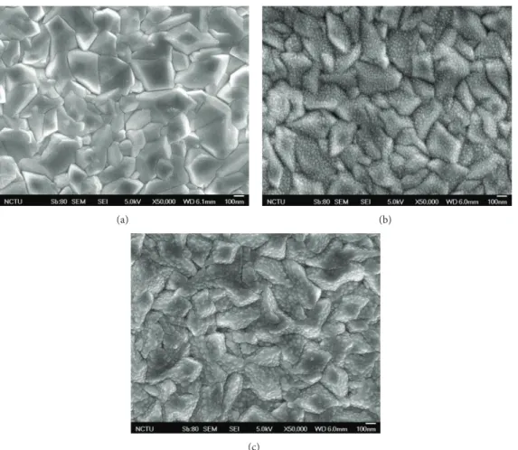
Figure 2 displays the plane-view SEM images of the textured FTO films with or without H2 plasma exposure. The sharp microstructures on the FTO films before H2 plasma exposure were approximately 100–500 nm in grain size. After the H2-plasma exposure for 72 seconds, the surface morphology exhibited many small particles (20– 30 nm in grain size) on the original FTO. As the time of H2 -plasma exposure increased to 900 seconds, the original FTO microstructures were damaged heavily and the size of small particles increased to 50 nm. These small particles may be ascribed to the reduction of the SnO2:F (FTO) surface which became SnO and metallic Sn with increasing the duration of plasma exposure [9]. The study also reported that the thickness of the surface layer of chemical reduction was found
(a) (b)
(c)
Figure 2: Plane-view SEM images of the textured FTO films (a) without H2plasma exposure, or with the H2plasma exposure for (b) 72 seconds and (c) 900 seconds.
to be 100 and 150 nm after H2-plasma (0.25 W/cm2, 13 Pa) exposure for 900 and 1800 seconds, respectively. In contrast, the surface damage and chemical reduction in our study would be more severe due to the higher power density and higher pressure (0.33 W/cm2, 500 Pa).
The combination of the optical, electrical, and structural results showed the FTO films were deteriorated after H2 -plasma exposure, which may be originated from the chemical reduction to form the metallic Sn or suboxides of SnO. To further identify the plasma-induced changes on the SnO2 surface, the survey spectra and high solution spectra of XPS were obtained. The measured signals including oxygen and carbon (a surface contaminant) were not shown for brevity. The Sn 3d5/2 peaks of high solution spectra as a function of H2 plasma exposure for FTO and AZO/FTO films were shown inFigure 3. A single Sn peak of the FTO without H2 -plasma exposure was observed at 487.0 eV. As the time of H2 -plasma exposure increased from 0 to 900 seconds, the main peak shifted to lower binding energy. Schade et al. reported that the core level peak of SnO2 is 487.0 eV, the main SnO peak is 486.7 eV, and the peak at 484.6 eV is due to elemental Sn [7]. These results confirmed that FTO film was reduced to the suboxide as SnO and metallic Sn with the increasing H2-plasma exposure duration. However, the AZO/FTO after 72-second H2-plasma exposure showed similar main peak at
492 490 488 486 484 482 0 5 486.7eV 484.6eV AZO/FTO-72 s-plasma FTO-900 s-plasma FTO-300 s-plasma FTO-72 s-plasma FTO-0s-plasma In te n si ty (a.u .)
Binding energy (eV) 487.0eV
Sn2+ Sn0
Sn4+
Figure 3: Sn 3d5/2signal of XPS spectrum as a function of H2plasma exposure time for FTO and AZO/FTO films.
487.0 eV compared to the FTO without H2-plasma exposure. This demonstrated that a layer of AZO can effectively protect the FTO films from chemical reduction during H2-plasma exposure.
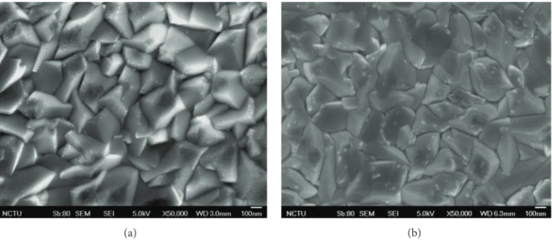
(a) (b)
Figure 4: Plane-view SEM images of the 5 nm AZO capped FTO films (a) without and (b) with 72-second H2-plasma exposure.
The plane-view SEM images of the surface morphology of 5 nm AZO layer capped FTO films with and without 72-second H2-plasma exposure are shown in Figure 4. Before 72-second H2-plasma exposure, the thin AZO layer covered well on the original FTO texture, as shown inFigure 4(a). Compared to the FTO films undergoing 72-second H2 -plasma exposure (shown inFigure 2(b)), the amount of the small particles on the original FTO microstructure arising from chemical reduction was significantly lowered by cap-ping the 5 nm-thick AZO, which is shown in Figure 4(b). Combined with the XPS results, this confirmed that 5 nm-thick AZO layer can prevent the FTO surface from the reduction of tin oxide and ion bombardment during H2 -plasma exposure. However, due to the less conductive nature of AZO material, the AZO film should be kept as thin as possible to retain the optoelectrical properties, while maintaining chemical reduction resistance. In this study, we have found that an optimized thickness of 5 nm-thick AZO film was obtained for the resistance to the hydrogen plasma as well as the cell performance. Based on the above results, the AZO/FTO structure with subsequent annealing in O2or N2environment at 200∘C was employed for the fabrication of 𝜇c-Si:H solar cells.
Figure 5provides the J-V characteristics of 1.2𝜇m-thick 𝜇c-Si:H single-junction cells using the FTO or AZO/FTO as front TCO with subsequent annealing in N2or O2 environ-ment. The p-i-n𝜇c-Si:H cell using only FTO exhibited a lower short circuit current density (𝐽SC) of 15.97 mA/cm2 and a
poor conversion efficiency of 5.69%. By using the unannealed AZO/FTO as front TCO, the𝐽SCincreased to 17.42 mA/cm2.
This was attributed to more optical transmission through the AZO/FTO substrate into the absorber due to the elimination of Sn reduction, which was confirmed by the results of optical transmission, as shown inFigure 1. However, the low efficiency and FF implied that the interface of TCO or TCO itself may need subsequent annealing for sputtered AZO. By using the AZO/FTO as front TCO with the subsequent annealing at 200∘C in O2environment for 0.5 hour, the p-i-n 𝜇c-Si:H cell exhibited a surprisingly enhanced 𝐽SCfrom 15.97
to 19.40 mA/cm2, and the increased conversion efficiency
0.0 0.1 0.2 0.3 0.4 0.5 0.6 0 4 8 12 16 20 (V) 5.69 70.52 15.97 0.51 0.50 17.42 68.43 5.96 5.96 63.41 18.42 0.51 7.09 71.63 19.40 0.52 AZO/FTO, AZO/FTO, AZO/FTO, no anneal FTO, no anneal Voltage (V) Voc Jsc FF Eff. C u rr en t den si ty (mA/cm 2) N2-0.5 hr-anneal O2-0.5 hr-anneal (%) (%) (mA/cm2)
Figure 5: J-V characteristics of 1.2𝜇m-thick 𝜇c-Si:H single-junction cells using the FTO or AZO/FTO with subsequent annealing in N2 or O2environment as front TCO.
from 5.69% to 7.09%. This significant enhancement was ascribed to the effective elimination of the Sn reduction on the FTO surface by the thin AZO layer during the Si-based thin-film deposition with hydrogen-rich plasma exposure. Moreover, the subsequent annealing of sputtered AZO could diminish the sputtering damage, leading to less defects and better interface of AZO/FTO. These results also corresponded to the quantum efficiency measurement, as demonstrated in
Figure 6.
Figure 6reveals the quantum efficiency (QE) of 1.2 𝜇m-thick p-i-n𝜇c-Si:H cells using the FTO or AZO/FTO as front TCO with subsequent annealing in N2or O2 environment. Compared to the 𝜇c-Si:H cell using only FTO, the quan-tum efficiency of the𝜇c-Si:H cell using AZO/FTO without annealing increased over wide wavelength range due to the suppression of the Sn reduction. The 0.5 hour annealing treatment of AZO/FTO in N2environment exhibited higher quantum efficiency than that of the AZO/FTO without annealing. The major QE enhancement at the wavelength
300 400 500 600 700 800 900 1000 1100 0 20 40 60 80 100 FTO, no anneal AZO/FTO, AZO/FTO, no anneal AZO/FTO, Qua nt um efficienc y (%) Wavelength (nm) O2-0.5 hr-anneal ( = 20.59 mA/cm2) N2-0.5 hr-anneal ( = 16.43 mA/cm2) (JSC JSC (JSC= 19.72 mA/cm2) JSC = 17.79 mA/cm2)
Figure 6: Quantum efficiency of 1.2𝜇m-thick p-i-n 𝜇c-Si:H single-junction cells using the FTO or AZO/FTO as front TCO with subsequent annealing in N2or O2environment.
from 550 to 1100 nm may originate from the increased transmission after annealing in N2environment due to the reduction in the density of grain boundaries [16]. Besides, it is observed that the AZO/FTO after annealing in O2 environment showed even higher quantum efficiency across whole measured wavelength than that in N2 environment, which might be ascribed to the higher transmission after annealing in O2 environment due to the decreased bulk defects and a small increase in bandgap [17]. By employing the AZO/FTO with O2annealing treatment for 0.5 hour, the 𝜇c-Si:H solar cell exhibited a relative enhancement of the QE of more than 25% compared to the FTO configuration without annealing.
4. Conclusion
The effects of H2 plasma exposure on optical, electrical, and structural properties of FTO and AZO/FTO substrates have been investigated. With increasing the time of H2 -plasma exposure, the hydrogen radical and ions penetrated through the FTO surface of chemical reduction to form more suboxides such as SnO and metallic Sn, which was confirmed by the XPS analysis. The Sn reduction on the FTO surface can be effectively eliminated by capping the FTO with a very thin layer of sputtered AZO (3–5 nm), as confirmed by the XPS analysis. By using the AZO/FTO as front TCO with the subsequent annealing, the p-i-n 𝜇c-Si:H cell exhibited a significantly enhanced𝐽SCfrom 15.97 to
19.40 mA/cm2 and an increased conversion efficiency from 5.69% to 7.09%. This significant enhancement was ascribed to the effective elimination of the Sn reduction on the FTO surface by the thin AZO layer during the Si-based thin-film deposition with hydrogen-rich plasma exposure. Moreover, the subsequent annealing of the sputtered AZO could lead to less defects as well as a better interface of AZO/FTO. The quantum efficiency of the AZO/FTO configuration cell
exhibited a relative enhancement of more than 25% compared to the FTO configuration without annealing.
Conflict of Interests
The authors do not have any conflict of interests with the content of the paper.
Acknowledgment
This work was supported by the National Science Council of Taiwan under Grant number 102-3113-P-008-001.
References
[1] J. Meier, R. Fl¨uckiger, H. Keppner, and A. Shah, “Complete microcrystalline p-i-n solar cell—crystalline or amorphous cell behavior,” Applied Physics Letters, vol. 65, no. 7, pp. 860–862, 1994.
[2] A. Shah, E. Vallat-Sauvain, P. Torres et al., “Intrinsic micro-crystalline silicon (𝜇c-Si:H) deposited by VHF-GD (very high frequency-glow discharge): a new material for photovoltaics and optoelectronics,” Materials Science and Engineering B, vol. 69-70, pp. 219–226, 2000.
[3] M. Kondo, “Microcrystalline materials and cells deposited by RF glow discharge,” Solar Energy Materials and Solar Cells, vol. 78, no. 1–4, pp. 543–566, 2003.
[4] A. V. Shah, J. Meier, E. Vallat-Sauvain et al., “Material and solar cell research in microcrystalline silicon,” Solar Energy Materials
and Solar Cells, vol. 78, no. 1–4, pp. 469–491, 2003.
[5] J. Koˇcka, “Relation of defects and grain boundaries to transport and photo-transport: solved and unsolved problems in micro-crystalline silicon,” Journal of Non-Crystalline Solids, vol. 358, pp. 1946–1953, 2012.
[6] R. B. Bergmann, T. J. Rinke, R. M. Hausner, M. Grauvogl, M. Vetter, and J. H. Werner, “Thin film solar cells on glass by transfer of monocrystalline Si films,” International Journal of
Photoenergy, vol. 1, no. 2, pp. 89–93, 1999.
[7] H. Schade, Z. E. Smith, J. H. Thomas III, and A. Catalano, “Hydrogen plasma interactions with tin oxide surfaces,” Thin
Solid Films, vol. 117, no. 2, pp. 149–155, 1984.
[8] J. H. Thomas III, “X-ray photoelectron spectroscopy study of hydrogen plasma interactions with a tin oxide surface,” Applied
Physics Letters, vol. 42, no. 9, pp. 794–796, 1983.
[9] S. Major, M. C. Bhatnagar, S. Kumar, and K. L. Chopra, “The degradation of fluorine doped tin oxide films in a hydrogen plasma,” Journal of Vacuum Science and Technology A, vol. 6, pp. 2415–2420, 1988.
[10] T. Minami, H. Sato, H. Nanto, and S. Takata, “Heat treatment in hydrogen gas and plasma for transparent conducting oxide films such as ZnO, SnO2and indium tin oxide,” Thin Solid Films, vol. 176, no. 2, pp. 277–282, 1989.
[11] J.-M. Themlin, M. Chta¨ıb, L. Henrard, P. Lambin, J. Darville, and J.-M. Gilles, “Characterization of tin oxides by x-ray-photoemission spectroscopy,” Physical Review B, vol. 46, no. 4, pp. 2460–2466, 1992.
[12] L. Raniero, I. Ferreira, A. Pimentel et al., “Role of hydrogen plasma on electrical and optical properties of ZGO, ITO and IZO transparent and conductive coatings,” Thin Solid Films, vol. 511-512, pp. 295–298, 2006.
Chen, “Mechanism of an AZO-coated FTO film in improving the hydrogen plasma durability of transparent conducting oxide thin films for amorphous-silicon based tandem solar cells,”
Journal of Materials Chemistry, vol. 22, no. 16, pp. 8005–8012,
2012.
[16] A. Mahmood, N. Ahmed, Q. Raza et al., “Effect of thermal annealing on the structural and optical properties of ZnO thin films deposited by the reactive e-beam evaporation technique,”
Physica Scripta, vol. 82, no. 6, Article ID 065801, 2010.
[17] O. Hamad, G. Braunstein, H. Patil, and N. Dhere, “Effect of thermal treatment in oxygen, nitrogen, and air atmospheres on the electrical transport properties of zinc oxide thin films,” Thin
Submit your manuscripts at
http://www.hindawi.com
Hindawi Publishing Corporation
http://www.hindawi.com Volume 2014 Inorganic Chemistry International Journal of
Hindawi Publishing Corporation
http://www.hindawi.com Volume 2014
Photoenergy
Hindawi Publishing Corporation
http://www.hindawi.com Volume 2014
Carbohydrate
Chemistry
International Journal of
Hindawi Publishing Corporation
http://www.hindawi.com Volume 2014 Journal of
Chemistry
Hindawi Publishing Corporation
http://www.hindawi.com Volume 2014
Physical Chemistry
Hindawi Publishing Corporation http://www.hindawi.com Analytical Methods in Chemistry Journal of Volume 2014 Bioinorganic Chemistry and Applications
Hindawi Publishing Corporation
http://www.hindawi.com Volume 2014
Spectroscopy
International Journal of Hindawi Publishing Corporationhttp://www.hindawi.com Volume 2014
The Scientific
World Journal
Hindawi Publishing Corporationhttp://www.hindawi.com Volume 2014 Medicinal Chemistry
Hindawi Publishing Corporation
http://www.hindawi.com Volume 2014
Chromatography Research International Hindawi Publishing Corporation
http://www.hindawi.com Volume 2014
Applied ChemistryJournal of
Hindawi Publishing Corporation
http://www.hindawi.com Volume 2014
Hindawi Publishing Corporation
http://www.hindawi.com Volume 2014
Theoretical Chemistry Journal of
Hindawi Publishing Corporation
http://www.hindawi.com Volume 2014
Journal of
Spectroscopy
Hindawi Publishing Corporation http://www.hindawi.com
Analytical Chemistry Volume 2014
Journal of Hindawi Publishing Corporation
http://www.hindawi.com Volume 2014 Quantum Chemistry Hindawi Publishing Corporation
http://www.hindawi.com Volume 2014 International
Hindawi Publishing Corporation
http://www.hindawi.com Volume 2014
Catalysts
Journal ofElectrochemistry
International Journal ofHindawi Publishing Corporation