高性能低溫多晶矽薄膜電晶體之製程技術與特性研究
296
0
0
全文
(2) 高性能低溫多晶矽薄膜電晶體之製程技術與特性研究. Study on the Process Technologies and Characteristics of High-Performance Low Temperature Polycrystalline Silicon Thin-Film Transistors. 研 究 生: 蔡春乾 指導教授: 鄭晃忠. 國. Student: Chun-Chien Tsai 博士. 立. 交. 電子工程學系. Advisor: Dr. Huang-Chung Cheng. 通. 大. 學. 電子研究所. 博 士 論 文. A Dissertation Submitted to Department of Electronics Engineering & Institute of Electronics College of Electrical Engineering and Computer Science National Chiao Tung University in partial Fulfillment of the Requirements for the Degree of Doctor of Philosophy in Electronics Engineering January 2008 Hsinchu, Taiwan, Republic of China. 中華民國 九十七 年 一 月.
(3) 高性能低溫多晶矽薄膜電晶體 之製程技術與特性研究. 研究生:蔡春乾. 指導教授:鄭晃忠. 博士. 國立交通大學電子工程學系暨電子研究所. 摘要 多晶矽薄膜電晶體因為具有較高的載子移動率,及可將周邊驅動電路與液晶面板積 體化至玻璃基板上來降低液晶顯示器之生產成本的優勢,使得它成為液晶顯示技術應用 中的關鍵元件,並且在高附加價值與多功能整合的系統面板(System-on-Panel)的應 用及三維積體電路(3-D ICs)的實現上具有很大的潛力。在現階段,採用準分子雷射退 火法對非晶矽薄膜進行再結晶是最有潛力的量產結晶技術,藉由達到快速熔融與固化再 結晶的方法,可得到一高品質的多晶矽薄膜並且可以保持玻璃基板不受到高溫的影響。 雖然透過準分子雷射可有效的提升多晶矽層的結晶性,但此方法仍有些許缺點,如隨機 的晶粒邊界及晶粒分佈、大晶粒的製程窗口較窄小、主動層和介電層之間造成大的粗糙 界面等等。在本篇論文裡,我們將提出多項雷射結晶方法及元件結構來增進低溫多晶矽 薄膜電晶體的特性。 首先,為了改善低溫多晶矽薄膜電晶體的電特性,我們先針對元件通道的多晶矽薄 膜結晶性進行改善。一種我們具有晶粒邊界位置控制的底閘極低溫多晶矽薄膜電晶體方 法將被提出而加以探討。其結晶機制敘述如下,因為底閘極結構邊緣台階區提供了較厚 非晶矽層,在準分子雷射退火時,我們只需將雷射能量控制在可以使薄區的非晶矽薄膜. i.
(4) 完全熔解的能量密度以上,同時讓厚區的非晶矽薄膜部分熔解而確保留下部分微晶矽作 為晶種,就可以得到一致分佈的大型晶粒成長,因此可以提升薄膜的均勻性及元件的效 能。由實驗的結果分析可知,我們可以得到最大長度約為 0.85μm 長的人為控制晶粒。 我們也製作出單一晶粒邊界的低溫多晶矽薄膜電晶體,其載子移動率可達到 330cm2 / V-s,同時閘極引起的汲極漏電和紐結效應也減少了,而且元件的均勻性也大幅提升。 而且在閘極偏壓的可靠度量測之下,我們發現單一晶粒邊界的底閘極低溫多晶矽薄膜電 晶體有較小的起始電壓漂移量及較高的崩潰電場,因此更適用於元件的微小化。 雖然單一晶粒邊界的底閘極低溫多晶矽薄膜電晶體表現出良好的電特性,由於偏離 的黃光微影製程,造成源極(汲極)相對於閘極的離子佈植不對稱,使的元件的電特性 不對稱。因此我們結合背後曝光方法與單一晶粒邊界的底閘極低溫多晶矽薄膜電晶體製 作出新穎之自我對準的單一晶粒邊界的底閘極低溫多晶矽薄膜電晶體。我們不僅包留了 單一晶粒邊界的底閘極低溫多晶矽薄膜電晶體的良好特性,自我對準的單一晶粒邊界的 底閘極低溫多晶矽薄膜電晶體也表現出良好的電對稱性。如此一來我們更能將自我對準 的單一晶粒邊界的底閘極低溫多晶矽薄膜電晶體應用於畫素電路中的開關元件。 將元件縮小,雖然可以進一步的提升多晶矽薄膜電晶體的電特性,但是也遭遇到嚴 重的短通道效應,尤其是薄膜電晶體因為本身通道較多的缺陷及低溫製程,短通道效應 更是較傳統金氧半場效電晶體明顯嚴重,因此雙閘極結構結合通道晶粒成長的技術也在 本論文提出,藉由該底閘極的準分子雷射結晶法,通道中的晶粒成長控制來得到較好的 結晶性,與上下雙閘極對通道的耦合來改善閘極對通道的控制能力,其 N 型元件以單 通道長度換算之等效載子移動率可超過 1000 cm2/V-s, 而 P 型元件則超過 400 cm2/V-s。此元件有高驅動電流,高開關電流比,優異的短通道抵抗力,較陡峭之次臨 界擺幅,較小的汲極誘導能障下降(DIBL),同時均勻性也得到改善。 雖然利用底閘極的準分子雷射結晶技術可以有效的改善多晶矽薄膜結晶性,但是不 可避免的,在低溫多晶矽薄膜電晶體的通道中存在一高角度的晶粒邊界,進而對於元件 電特性造成劣化及耐用度上的問題。因此我們提出了一個新穎的側向雷射結晶方式-間 隙壁式結晶法-來消彌通道中的高角度的晶粒邊界,其結晶機制是利用空間上的熱傳機 ii.
(5) 制來達成晶粒橫向成長的目的,首先利用傳統間隙壁法製作出 50 奈米大小的晶種,並 在局部微小區域產生兩種厚度不同的非晶矽薄膜,當準分子雷射照射在此一結構上,使 較薄的區域完全熔融時,而間隙壁較厚的區域部分熔解,晶粒便會以這些非晶矽間隙壁 為結晶起始點,做橫向成長,再藉由適當的安排間隙壁與元件通道的相關位置,我們將 可以消除通道中所有垂直電流方向的晶粒邊界,更進一步的改善元件的載子移動率與均 勻性。以通道長度為 2 µm 的元件為例,以此結晶方法做出的低溫多晶矽薄膜電晶體其 載子移動率可以到達 288 cm2/V-s,而傳統的元件的載子移動率只有 129 cm2/V-s.。 為了更進一步的提升多晶矽薄膜電晶體的驅動能力,達到一類似絕緣層上覆晶矽 (Silicon-On-Insulator-like)金氧半場效電晶體的效能,進而實現 SOP 或 3D ICs 的夢想, 無晶粒邊界的單晶矽電晶體(Single-grain TFT)是最終目標的元件,因此我們提出了 一個新穎的二維晶粒控制側向成長的雷射結晶方式,結合上述之非晶矽間隙壁及先定義 矽薄膜之結晶法來分別達成 X 軸及 Y 軸的熱梯度,進而完成單晶粒之側向晶粒成長。從 實驗分析結果發現,我們可以得到一直徑為 1.8 µm 大的圓型週期性單晶粒矽薄膜。以 通道長度為 1.5 µm 的元件為例,以此結晶方法做出的低溫多晶矽薄膜電晶體其載子移 動率可以到達 308 cm2/V-s,開關電流比則高於 108,且具高度的均勻性。 上述的結晶法雖然可以達成大晶粒成長及高性能薄膜電晶體的目的,而本論文亦提 出一新式的固態連續波雷射(Continuous-wave Laser)退火技術,直接利用控制掃瞄速 度及掃瞄功率來達成晶粒橫向成長。一長度達 15 µm 的多晶矽薄膜晶粒可以製作出來而 不損傷到玻璃基板,而實驗結果亦顯示矽薄膜具有極佳的結晶性,同時其晶粒邊界位置 的表面粗糙度極為平順。利用連續波雷射結晶法製作的低溫多晶矽薄膜電晶體擁有優異 的電特性,例如較高的電子移動率(n 通道的其載子移動率可達 500cm2/V-s,而 p 通道 的為 200cm2/V-s)及較高的開關電流比。另外,我們也探討了利用連續波雷射在摻雜活 化的退火特性,其由四點探針分析可得一片電阻低於 50 Ω/□,同時由二次離子質譜 分析儀得到一均勻分佈的摻雜雜質,因此連續波雷射退火法是一個低熱預算和高效率的 活化方法。由於連續波雷射結晶法製作大晶粒流程十分簡單,因此使用連續波結晶法製 作的低溫多晶矽薄膜電晶體的亦極適合於未來系統面板的應用。 iii.
(6) Study on the Process Technologies and Characteristics of High-Performance Low Temperature Polycrystalline Silicon Thin-Film Transistors Student: Chun-Chien Tsai. Advisor: Dr. Huang-Chung Cheng. Department of Electronics Engineering & Institute of Electronics National Chiao Tung University. ABSTRACT. Low-temperature polycrystalline silicon (LTPS)thin film transistors (TFTs) have been extensively studied for active matrix flat panel displays (AMFPDs), full-function system-on-panel (SOP), and potential for the 3-dimensional integrated circuits (3D-ICs) applications owing to their high field-effect mobility, low power consumption, high reliability, high resolution, and low fabrication cost by the integration of driver and controller ICs. At this moment, excimer laser crystallization (ELC) of amorphous silicon (a-Si) thin films seems to be the most promising method for its great advantages in mass production and high quality silicon grains without damage to the glass/plastic substrates. Although large grains can be attained in the super lateral growth (SLG) regime by ELC, many fine grains still spread between these large grains due to the narrow process window for producing large-grain poly-Si and highly rough interface. Consequently, non-uniform and randomly distributed poly-Si grains will result in the large variation of TFT performance when the laser energy density is controlled in the SLG regime, especially for the small-dimensional TFTs. In this iv.
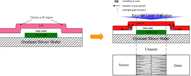
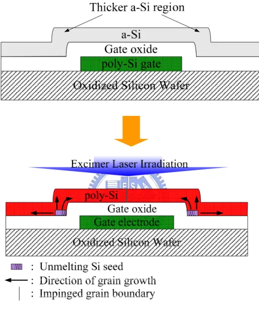
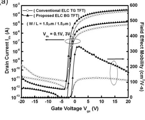
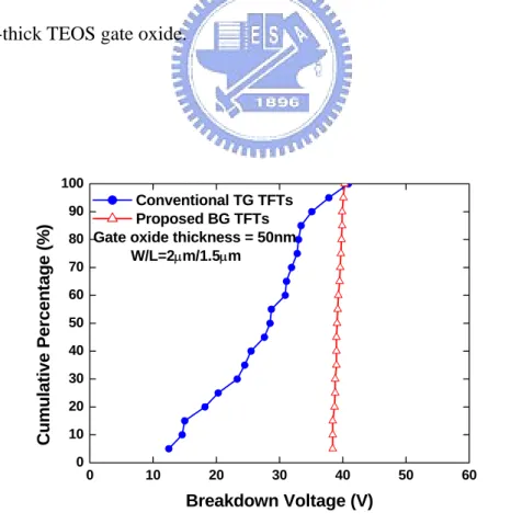
(7) thesis, many approaches, including techniques of excimer-laser-crystallized poly-Si thin films, advanced device structures, and diode-pumped solid-state (DPSS) continuous-wave (CW) laser annealing, have been proposed to further enhance the performance of LTPS TFTs. At first, from the perspective of improving channel material quality, LTPS TFTs with bottom gates (BG) have been demonstrated to achieve large silicon grains due to the lateral grain growth. In this method, a-Si thin film with two kinds of thicknesses in a local region was formed by the deposition of a-Si films on the plateau structure. When the excimer laser irradiation is applied on the a-Si thin film, the applied laser energy density is controlled to completely melt the thin region of a-Si film in the channel region but partially melted the thick region of a-Si film near the edges of bottom gate. Therefore, a lateral temperature gradient can be produced between the local thin and thick regions of a-Si film, and the lateral grain growth started from the un-melted silicon solid seed at the base neighbor to the bottom-gate corner, and extended toward the completely melted region until the solid-melt interface from opposite direction impinges. From material analyses, it can be observed that the large longitudinal grains artificially grown of about 0.85 µm in size were observed in the device channel region. Therefore, high-performance BG LTPS-TFTs have been demonstrated with the field-effect mobility exceeding 330cm2/V-s, low GIDL effect, suppressed kink current, and improved device uniformity due to the large silicon grains. Moreover, the BG TFTs reveal higher breakdown voltage and better reliability due to the smooth interface between gate dielectric and poly-Si channel films as thinner gate oxide were employed without additional processes or materials. The improved breakdown and driving characteristics imply that the proposed BG-TFT structure is more suitable for the device-scaled-down applications. Although BG LTPS-TFTs exhibit superior electrical characteristics, asymmetrical electrical characteristics are also observed due to the misaligned process effect. Therefore, a self–aligned (SA) bottom-gate TFT with appropriate channel length has been fabricated by v.
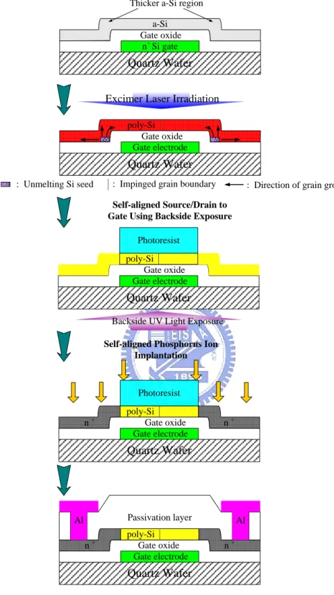
(8) the simple ELC and backside exposure. As a result, not only all the advantages of BG LTPS-TFTs with lateral silicon grains, but also the symmetrical electrical characteristics can be also observed in SA BG LTPS-TFTs. Consequently, SA-BG TFTs with the channel length of 1 µm exhibited field-effect-mobility reaching 193 cm2/Vs without hydrogenation, while the mobility of the conventional non-SA-BG TFTs and conventional SA top-gate ones were about 17.8 cm2/Vs and 103 cm2/Vs, respectively. Shrinking the device size is an effective way to improving the device performance, but poor short-channel effects (SCE) is encountered owing to the insufficient gate controllability. Novel high-performance LTPS TFTs with double-gate (DG) structure and controlled lateral grain growth have been demonstrated by excimer laser crystallization. Because of the double gate operation mode and lateral silicon grains formed in the channel region, the devices have a higher driving current, steeper subthreshold slope, superior short-channel effect immunity, and suppression of the floating-body effect. The proposed DG TFTs (W/L = 1/1 µm) have the equivalent field-effect-mobility exceeding 1050 cm2/Vs for the N-channel device, 403 cm2/Vs for the P-channel device, on/off current ratio higher than 109, smaller DIBL, and excellent device uniformity. Although the crystallinity of poly-Si thin film can be effectively enhanced via ELC with bottom-gate structure, it is inevitable that there is a high angle grain boundary in the middle of channel region, which degrades the TFT performance and reliability. A novel laser crystallization method which can remove the high angle grain boundary and produce the large and uniform grains in the desired local region is proposed to improve the field-effect mobility as well as the device uniformity. Periodically lateral silicon grains with 2 µm in length can be artificially grown in the channel regions via the amorphous silicon spacer structure with excimer laser irradiation. By the way, such periodically large and lateral grains in the TFTs would achieve high field-effect mobility of 298 cm2/Vs, as compared with the conventional ones of 128 cm2/Vs. In addition, the device-to-device uniformity could be improved due to vi.
(9) this location-manipulated lateral silicon grains. In order to further improve the performance of LTPS TFTs, single-grain TFT in which the channel is grain-boundary-free will exhibit SOI-like performance to satisfy the requirements of system on panel. A new crystallization technology for producing two-dimensional lateral grain growth, aiming at single-grain TFT, has been developed by excimer laser irradiation relying on the spatially temperature distribution at the artificially sites. The high quality silicon grains are controlled via manipulating super lateral growth phenomenon by spatially two kinds of silicon films and pre-patterned structure. An array of 1.8-µm-sized disklike silicon grains is formed periodically. Not only high-performance poly-Si TFTs with field-effect-mobility reaching 308 cm2/Vs but also excellent device uniformity are demonstrated owing to the artificially-controlled lateral grain growth. Proposed poly-Si TFTs, therefore, have great potential for the future SOP and 3D-ICs applications. Although the aforementioned laser crystallization methods can fabricate large homogeneous silicon grains and high-performance LTPS TFTs, another crystallization approach, a new and simple CW laser crystallization, is also proposed to produce lateral grain growth via controlling the laser scanning speed and laser power. According to the experimental results, a directional river-like lateral Si grain growth with tens of micron, flat surface morphology, and excellent crystallinity are achieved without damage to the glass substrates. As a result, ultra-high performance CW laser-annealed LTPS-TFTs have been fabricated on the oxidized silicon wafer for the first time with field-effect mobility exceeding 504 cm2/V-s for n-channel devices and 220 cm2/V-s for p-channel devices. It is also found that CW laser annealing is a low-thermal-budget and high-efficiency dopant activation method attributed to the low sheet resistance and uniformly redistributed dopant profiles after CW laser annealing. Because of the simple process, continuous-wave laser-annealed LTPS TFTs are very promising for the future SOP, 3D-ICs, and solar cell applications. vii.
(10) 誌. 謝. 感謝我的論文指導教授 鄭晃忠博士在實驗、研究與論文上的熱心且詳實的指導, 老師嚴謹認真的研究態度以及謙恭溫和的待人處事,都讓學生獲益良多,老師耐心的教 誨與鼓勵,也使我能順利完成博士學位。 感謝常鼎國學長與林敬偉學長帶領我進入低溫多晶矽薄膜電晶體的研究領域,給予 充分熱心的實驗訓練幫助及研究觀念上的指導,也由衷的感謝陳旭信學弟、韋凱方學 弟、曾煥均學弟、陳彥佑學弟、張為鈞學弟在實驗及計畫上的幫忙及支援,同時感謝李 逸哲同學、李序恆學弟、楊柏宇學弟、李耀仁學長、林家彬學長在行政及生活上的幫忙 與協助;使得本論文研究得以順利的完成。 感謝實驗室的學長、同學、學弟妹及助理們,謝謝你們在實驗或是生活上都能夠給 予我支持與關心,使得我的研究能夠順利完成,其中包含了王志良學長、阮全平學長、 陳國基學長、張芳龍學長、張國瑞學長、曾章和學長、張原熏學長、朱芳村學長、林高 照同學、陳柏廷學弟、賴瑞霖學弟、呂健豪學弟、江可玉學妹、郭育如學妹、魏瑛君學 妹、廖大傳學弟、許鈞凱學弟、林君翰學弟、王祐圻學弟、陳俠威學弟、高翠敏助理、 簡秀芳助理、李瑩姿助理、凌碧蓮助理、張依婷助理、楊宜樺助理以及其他學長、同學、 學弟妹們,有了你們在生活上的相伴和打氣,此論文才能順利完成。 感謝國立交通大學奈米中心及國家奈米元件實驗室提供優良的設備與研究環境,尤 其要感謝彭兆光先生、吳政三先生、徐秀鑾小姐、陳明麗小姐、黃月美小姐、陳聯珠小 姐、陳悅婷小姐、彭馨誼小姐、倪月珍小姐、范秀蘭小姐、林素珠小姐、徐台鳳小姐、 劉曉玲小姐及何惟梅小姐等,在製程、設備及分析上的大力協助。也感謝諸位口試委員 的指導與建議。 感謝我敬愛的父母 蔡神祐先生與陳蓮枝女士,謝謝你們多年來辛苦的培育我,教 育我,有了你們持續的支持與默默的付出,才能讓我得以全心投入學業,完成博士學位, 同時也要感謝我的妹妹 蔡月霜以及弟弟 蔡育修,在家中生活上的幫忙扶持。 感謝我的太太 辜郁雯在我研究生生涯中無悔的支持我,不論晴雨,一路相隨;也 感謝太太娘家家人的對我的鼓勵與信任,由衷的感謝你們。 最後感謝所有曾經幫助過我的朋友們,謝謝你們一路上給我的支持與關心。. viii.
(11) Contents Abstract (in Chinese). i. Abstract (in English). iv viii. Acknowledgments (in Chinese). ix. Contents Table Captions. xiv. Figure Captions. xvii. Chapter 1. Introduction .....……………………………………………………1. 1.1. The Evolution of Silicon-Based Thin-Film Transistors………………………….1. 1.2. TFT Structure…………………………………………………………………….3. 1.3. Approaches to the Preparation of Polycrystalline Silicon Thin Films…………...5 1.3.1. Solid Phase Crystallization for Poly-Si Thin Films………………………5. 1.3.2. Metal Induced Crystallization for Poly-Si Thin Films……………………6. 1.3.3. Laser Crystallization for Poly-Si Thin Films……………………………..8. 1.4. Ion Doping and Activation……………………………………………………...13. 1.5. Motivation………………………………………………………………………15. 1.6. Thesis Organization…………………………………………………………….18. Chapter 2. High-Performance Low Temperature Polycrystalline Silicon Thin-Film Transistors Crystallized by Excimer Laser Irradiation with Bottom-Gate Structure……………………………………...25. ix.
(12) 2.1. Introduction…..…………………………………………………..………………25. 2.2. The Concept of Controlled Lateral Grain Growth with Bottom-Gate structure...30. 2.3. Experiments……….…………………………………………………………......31 2.3.1. The Setup of Excimer Laser Crystallization System……………………..31. 2.3.2. Sample Preparation for Material Analysis………………………………..32. 2.3.3. Fabrication of Bottom-Gate LTPS TFTs using ELC……………………...33. 2.4. Results and Discussion…………………………………………………………...35 2.4.1. Material Characterization of ELC Poly-Si Thin Films with Bottom-Gate Structure……....…………………………………………………………..35. 2.4.1.1. Scanning Electron Microscopy (SEM) Analysis………………….36. 2.4.1.2. Atomic Force Microscopy (AFM) Analysis………………………40. 2.4.1.3. Transmission Electron Microscopy (TEM) Analysis…………..….40. 2.4.1.4. Secondary Ion Mass Spectroscopy (SIMS) Analysis……………...41. 2.4.2. Electrical Characteristics of LTPS TFTs Fabricated Using Excimer Laser Irradiation with Bottom-Gate Structure…………………………………..42. 2.5. Summary…………………………………………………………………………46. Chapter 3. High-Performance Self-Aligned Bottom-Gate Low Temperature Polycrystalline Silicon Thin-Film Transistors with Excimer Laser Crystallization……………………………………………………64. 3.1. Introduction………………………………………………………………………64. 3.2. Experiments……………………………………………………………………...66. 3.3. 3.2.1. Sample Preparation for Material Analysis …………………………….....66. 3.2.2. Fabrication of Self-Aligned (SA) BG LTPS TFTs using ELC…………...67. Results and Discussion…………………………………………………………..69 x.
(13) 3.3.1. Material Characterization of SA-BG LTPS Thin Films………………….69 Optical Microscopy (OM) Analysis………………………………69. 3.3.1.2. Scanning Electron Microscopy (SEM) Analysis………………….70. 3.3.1.3. Transmission Electron Microscopy (TEM) Analysis……………..71. 3.3.2. 3.3.1.1. 3.4. Electrical Characteristics of SA-BG LTPS TFTs using ELC…………….73. Summary………………………………………………………………………....75. Chapter 4. High-Performance Short-Channel Double-Gate Low Temperature Polycrystalline Silicon Thin-Film Transistors Using Excimer Laser Crystallization……………………………………………. 89. 4.1. Introduction……………………………………………………………………...89. 4.2. Experiments……………………………………………………………………...91. 4.3. Results and Discussion…………………………………………………………..93 4.3.1. Material Characterization of Excimer Laser-Crystallized Double-Gate Low-temperature Poly-Si Thin Films Transistors………………………...93. 4.3.2. Electrical Characterization of Excimer Laser-Crystallized Double-Gate Low-temperature Poly-Si Thin Films Transistors………………………...95. 4.4. Summary………………………………………………………………………..101. Chapter 5. Periodically Lateral Silicon Grains Fabricated by Excimer Laser Irradiation with Amorphous Silicon Spacers and Its Application to High-Performance Low Temperature Polycrystalline Silicon Thin Film Transistors…………………………………………..119. 5.1. Introduction. …………………………………………………………………119 xi.
(14) 5.2. The Basic Concept of Periodically Lateral Silicon Grains Employing Excimer Laser Crystallization with a-Si Spcaer Structures……………………………..120. 5.3. Experiments…………………………………………………………………….122. 5.4. Results and Discussion ………………………………………………………...123 5.4.1. Material Characterization of ELC Poly-Si Thin Films with a-Si Spacer Structure…………………………………………………………………123. 5.4.2. Electrical Characteristics of LTPS TFTs Fabricated Using Excimer Laser Irradiation with a-Si Spacer Structure…………………………………...125. 5.5. Summary………………………………………………………………………..127. Chapter 6. Low Temperature Polycrystalline Silicon Thin-Film Transistors on Location-Controlled Silicon Crystal Grains Fabricated by Pre-Patterned Silicon Films with A-Si Spacers using Excimer Laser Irradiation………………………………………………..141. 6.1. Introduction……………………………………………………………………..141. 6.2. Experiments…………………………………………………………………….142. 6.3. Results and Discussion………………………………………………………....145. 6.4. Summary………………………………………………………………………..150. Chapter 7. Ultra High-Performance Low Temperature Polycrystalline Silicon Thin-Film Transistors Fabricated via Diode-Pumped Solid-State Continuous Wave Laser Annealing…………………………….159. 7.1. Introduction……………………………………………………………………..159. 7.2. Experiments…………………………………………………………………….162. 7.3. Results and Discussion…………………………………………………………164 xii.
(15) 7.3.1. Material Characterization of Poly-Si Thin Films Crystallized by Diode-Pumped Solid-State Continuous Wave Laser…………………....164. 7.3.2. Crystallization Mechanism of Diode-Pumped Solid-State Continuous Wave Laser-Crystallized Poly-Si Thin Films………………………………….171. 7.3.3. Electrical Characteristics of LTPS TFTs Fabricated Using Diode-Pumped Solid-State Continuous Wave Laser Annealing…………………………172. 7.4. Summary………………………………………………………………………..175. Chapter 8. Summary and Conclusions……………………………………..195. Chapter 9. Future Prospects………………………………………………..201. References…………………………………………………………………....204 Publication Lists Vita. xiii.
(16) Table Captions. Chapter 1. Table 1-1. The system-on-panel (SOP) technology roadmap where LTPS TFT performances and related processes are going on in the features……………………………..21. Chapter 2. Table 2-1. Measured electrical characteristics of bottom-gate LTPS TFTs and conventional top-gate ones…………………………………………………………………...48. Table 2-2. Measured electrical characteristics of bottom-gate LTPS TFTs and conventional top-gate ones. (W = L = 1.5 µm and gate oxide thickness of 500 Å or 1000 Å………………………………………………………………………………..48. Chapter 3 Table 3-1. Measured electrical characteristics of SA-BG LTPS TFTs with lateral grain growth and conventional non-SA BG ones…………………………………...77. Chapter 4 Table 4-1. Measured electrical characteristics of ELC DG TFTs with lateral grain growth, SPC DG TFTs, and conventional ELC TG TFTs………………………..…103. Table 4-2. Measured electrical characteristics of ELC DG TFTs with high-temperature xiv.
(17) LPCVD gate oxide and ELC DG TFTs with low-temperature PECVD gate oxide………………………………………………………………………..103 Table 4-3. Measured electrical characteristics of high-temperature processed n-channel and p-channel ELC DG TFTs with lateral grain growth…………………...104. Table 4-4. Measured electrical characteristics of ELC DG TFTs with lateral grain growth, ELC TG TFTs with lateral grain growth, and ELC BG TFTs with lateral grain growth……………………………………………………………………...104. Chapter 5. Table 5-1. Measured electrical characteristics of LTPS TFTs crystallized with a-Si spacer and conventional structures……………………………………………………129. Table 5-2. Measured optimal electrical characteristics of LTPS TFTs crystallized with conventional and a-Si spacer structures, respectively…………………………130. Chapter 6. Table 6-1. Measured electrical characteristics of poly-Si TFTs with location-controlled (LC) silicon grains and conventional TFTs with random grain structure…………...151. Chapter 7. Table 7-1 The comparisons of excimer laser and DPSS continuous wave laser………...177 Table 7-2 Measured sheet resistance of samples after various activation methods……...177 Table 7-3 Measured electrical characteristics of LTPS TFTs crystallized by DPSS CW laser and excimer laser……………………………………………………………..178. xv.
(18) Table 7-4 Comparisons of CWC TFTs channel length structurally parallel and perpendicular to the direction of laser scanning……………………………..178. xvi.
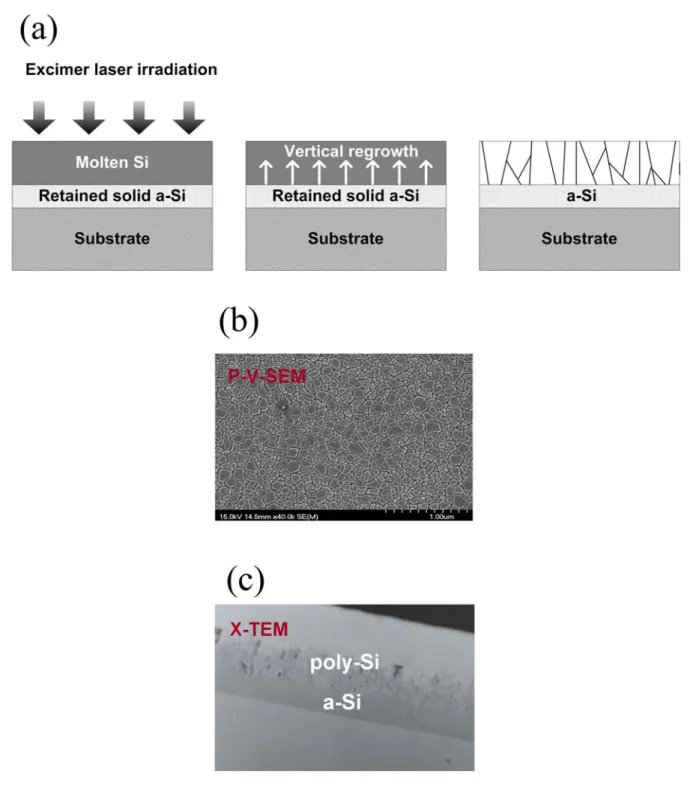
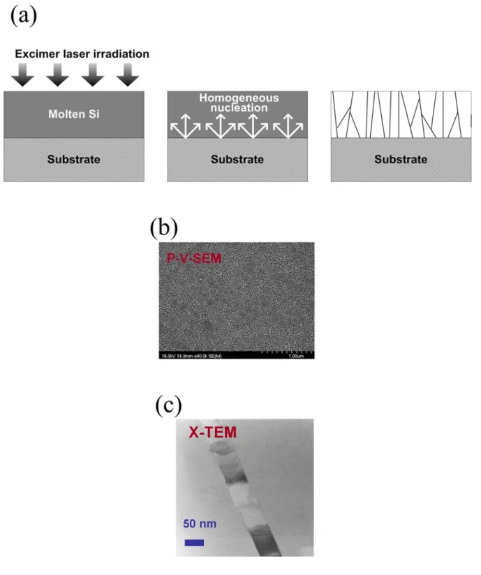
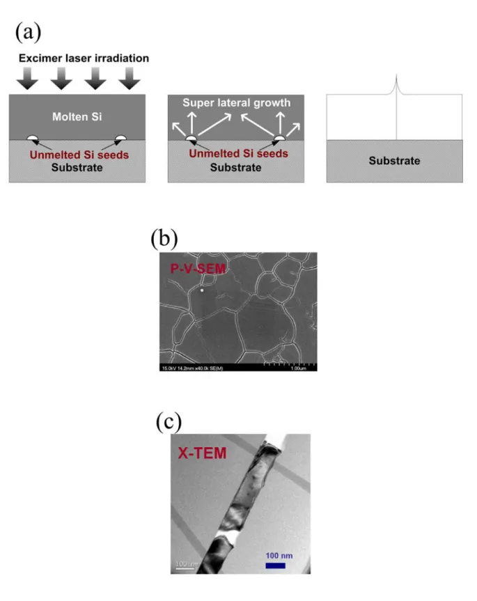
(19) Figure Captions. Chapter 1. Fig. 1-1.. (a) The schematic illustration of the low-energy density regime corresponding to energy densities that partially melt the a-Si thin film. (b) The plane-view scanning electron micrograph (SEM) and (c) cross-sectional transmission electron micrograph (TEM) of excimer-laser- crystallized poly-Si thin films in the partial-melting regime, respectively……………………………………………...22. Fig. 1-2.. (a) The schematic illustration of the high-energy density regime corresponding to energy densities that completely melt the a-Si thin film. (b) The plane-view scanning electron micrograph (SEM) and (c) cross-sectional transmission electron micrograph (TEM) of excimer-laser- crystallized poly-Si thin films in the complete-melting regime, respectively…………………………………………..23. Fig. 1-3.. (a) The schematic illustration of the near-complete-melting regime corresponding to energy densities that near completely melt the a-Si thin film. (b) The plane-view scanning electron micrograph (SEM) and (c) cross-sectional transmission electron micrograph (TEM) of excimer-laser- crystallized poly-Si thin films in the near-complete-melting regime, respectively……………………………………...24. Chapter 2. Fig. 2-1.. The schematic illustration of the mechanism of lateral grain growth using. xvii.
(20) bottom-gate structure of a-Si thin film……………………………………………49 Fig. 2-2.. The schematic illustration of excimer laser crystallization system……………….49. Fig. 2-3.. The process procedures for the preparation of poly-Si thin films with bottom-gate structure crystallized by ELC……………………………………………………..50. Fig. 2-4.. The key processes for fabricating short channel bottom-gate LTPS TFTs with excimer laser annealing…………………………………………………………...51. Fig. 2-5.. (a) The schematic cross-sectional drawing of conventional top- gate LTPS TFTs using the super lateral growth (SLG) excimer laser annealing condition. (b) Plane-view SEM micrograph of excimer laser crystallized poly-Si thin film with SLG laser annealing condition after Secco-etch………………………………….52. Fig. 2-6.. The SEM micrographs of excimer laser crystallized poly-Si thin films with bottom-gate structure after Secco etching, in which the device channel length was (a) 1.2 µm, (b) 1.5 µm, and (c) 2.0 µm, respectively. In this case, the laser shot number is single pulse and the poly gate thickness was 1000 Å. The laser energy density is 450 mJ/cm2…………………………………………………………….53. Fig. 2-7.. Scanning electron microscope micrographs of excimer laser crystallized poly-Si thin film with bottom-gate structure after Secco-etch, in which the device channel length was 1.5µm, and the laser shot number was (a) 1shot, (b) 20 shots, and (c) 100 shots, respectively………………………………………………….54. Fig. 2-8.. Scanning electron microscope micrographs of excimer laser crystallized poly-Si thin film with bottom-gate structure after Secco-etch, in which the device channel length was 1.5µm, and the laser energy density was (a) 430, (b) 450, and (c) 490 mJ/cm2, respectively……………………………………………………55. Fig. 2-9.. The SEM micrographs of poly-Si thin films irradiated by excimer laser shot number of 20 shots and the gate oxide thickness of (a) 30, (b) 50, and (c) 100 nm, respectively, in which the device channel length was 1.5 µm. The laser energy xviii.
(21) density is 450 mJ/cm2…………………………………………………………….56 Fig. 2-10. The SEM micrographs of poly-Si thin films irradiated by excimer laser shot number of 20 shots and the bottom-gate thickness of (a) 100, (b) 200, and (c) 300 nm, respectively, in which the device channel length was 1.5 µm………...57 Fig. 2-11. The AFM image of 1000 Å-thick poly-Si thin films with bottom-gate structure after laser crystallization, in which the device channel length is 1.5 µm. In this case, the laser shot number is 20 shots and the bottom-gate thickness is 1000 Å………………………………………………………………………………...58 Fig. 2-12. The cross-sectional TEM image of 1000 Å-thick poly-Si thin films with bottom-gate structure after laser crystallization, in which the device channel length is 1.5 µm…………………………………………………………………58 Fig. 2-13. The element SIMS depth profiles of the excimer laser-crystallized bottom-gate TFTs…………………………………………………………………………….59 Fig. 2-14. Comparisons of (a) Transfer characteristics and (b) Output characteristics for ELC BG LTPS TFT with lateral silicon grains and conventional ELC TG TFT.......................................................................................................................60 Fig. 2-15. Dependence of field-effect-mobility on the device dimension for ELC BG LTPS TFTs with lateral silicon grins and conventional ELC TG ones. The field effect mobility was evaluated at Vds = 0.1 V…………………………………………..61 Fig. 2-16. Dependence of field-effect-mobility on applied laser energy density for ELC BG TFTs with lateral silicon grins and conventional ELC TG ones with random grain structures………………………………………………………………….61 Fig. 2-17. (a) Comparison of the transfer characteristics of the n-channel LTPS BG-TFTs with lateral silicon grains and conventional TG ones with W = L = 1.5 µm and gate oxide thickness of 500 Å or 1000 Å. (b) Comparison of the output characteristics of the n-channel LTPS BG-TFTs with lateral silicon grains and xix.
(22) conventional TG ones with W = L = 1.5 µm and gate oxide thickness of 500 Å or 1000 Å…………………………………………………………………………..62. .Fig. 2-18. (a) The gate-breakdown voltage of two different TFT structures with 500 Å-thick TEOS gate oxide. (b) Statistical distribution of the gate-breakdown voltage of two different TFT structures with 500 Å-thick TEOS gate oxide………………63. Chapter 3. Fig. 3-1.. The process procedures for the preparation of self-aligned bottom-gate structure with large silicon grains by the excimer laser crystallization and the backside exposure…………………………………………………………………………..78. Fig. 3-2.. The key process procedures for fabricating small-dimension self-aligned bottom-gate LTPS TFTs with lateral grain growth……………………………….79. Fig. 3-3.. The optical microscope (OM) images of the samples with bottom gate structure from the transparent light source. The thickness of the amorphous silicon gate electrode was both 1000Å and the channel length was (a) 2 µm and (b) 5 µm, respectively……………………………………………………………………….80. Fig. 3-4. OM images of (a) the non-self-aligned and (b) the self-aligned ion-implanted devices after photo-lithography from the reflected light source, in which the channel length was 2 µm………………………………………………………….81 Fig. 3-5.. The SEM micrographs of the self-aligned ion-implanted devices after the photo-lithography…………………………………………………………………82. Fig. 3-6.. (a) Scanning electron microscope micrograph of excimer laser crystallized poly-Si film with bottom-gate structure on quartz wafer after Secco etching, in which the. xx.
(23) thickness of bottom-gate electrode was 100 nm. (b) Scanning electron microscope micrograph of excimer laser crystallized poly-Si film with bottom-gate structure on quartz wafer after Secco etching, in which the thickness of bottom-gate electrode was 150 nm…………………………………………..83 Fig. 3-7.. (a) FIB-prepared cross-sectional TEM images and the diffraction patterns of laser-crystallized poly-Si thin films of the self-aligned bottom-gate devices. (b) High-magnification cross-sectional bright-field TEM image and the selected-area electron diffraction pattern of laser-crystallized poly-Si thin films of the self-aligned bottom-gate devices…………………………………………………84. Fig. 3-8.. (a) The typical transfer characteristics of SA BG LTPS TFTs with bottom-gate thickness of 1000 Å and 1500 Å, respectively. (b) The output characteristics of SA BG LTPS TFTs with bottom-gate thickness of 1000 Å and 1500 Å, respectively……………………………………………………………………….85. Fig. 3-9.. (a) Comparison of the transfer characteristics between the SA-BG LTPS TFTs and conventional non-SA-BG ones with W = L = 1 µm. (b) Comparison of the output characteristics between the SA-BG LTPS TFTs and conventional non-SA-BG ones with W = L = 1 µm………………………………………………………………..86. Fig. 3-10. Experimental measured bi-directional transfer characteristics of SA-BG TFT and conventional one under the polarities of the source and drain are interchanged……………………………………………………………………..87 Fig. 3-11. (a) Experimental measured bi-directional output characteristics of SA-BG TFT under the polarities of the source and drain are interchanged. (b) Experimental measured bi-directional output characteristics of non-SA-BG TFT under the polarities of the source and drain are interchanged……………………….87 & 88. xxi.
(24) Chapter 4. Fig. 4-1.. The schematic cross-sectional view of the different poly-Si TFT devices. (a) Conventional n-channel top-gate TFT and (b) n-channel DG TFT……………..105. Fig. 4-2.. The key fabrication process steps for the proposed short-channel double-gate LTPS TFTs structure crystallized with excimer laser annealing………………………106. Fig. 4-3.. (a) The optical micrograph, (b) the bird-eye SEM graph, and (c) the cross-sectional SEM graph of proposed excimer-laser-crystallized double-gate LTPS TFTs…..107. Fig. 4-4. The cross-sectional TEM photograph of connection of the top-gate electrode and the bottom-gate electrode and energy dispersive X-ray (EDX) Spectrometer analysis…………………………………………………………………………..108 Fig. 4-5. Atomic force microscopy (AFM) images of poly-Si thin film with bottom-gate structure after laser irradiation…………………………………………………..109 Fig. 4-6.. Scanning electron microscope (SEM) micrographs of excimer laser crystallized poly-Si film with bottom-gate structure after Secco etching, in which the device channel length was (a) 1.2, (b) 1.5, and (c) 2 µm, respectively…………………110. Fig. 4-7.. The cross-sectional TEM image and the selected-area electron diffraction patterns of the fabricated ELC double-gate poly-Si TFTs. The channel length of DG TFTs is 1.2 µm. The thickness of top-gate electrode, top-gate oxide, poly-Si channel layer, bottom-gate oxide, and the bottom-gate electrode all are 100 nm. The insets show the top-view SEM graph and the high-resolution cross-sectional TEM image of the grain boundary region……………………………………………111. Fig. 4-8.. (a) Transfer characteristics of proposed ELC DG TFT, conventional SPC DG TFT, and conventional ELC TG TFT. (b) Output characteristics of proposed ELC DG TFT, conventional SPC DG TFT, and conventional ELC TG TFT……………112. xxii.
(25) Fig. 4-9.. Plot of ln(ID/VGS) versus 1/(VGS) curves at VDS = 0.1 V and high VGS for DG poly-Si TFTs and conventional TG ones………………………………………113. Fig. 4-10. FIB-prepared cross-sectional TEM image of excimer laser crystallized DG poly-Si TFTs……………………………………………………………………113 Fig. 4-11. The dependence of field effect mobility on temperature for ELC DG TFTs with lateral silicon grains, ELC TG TFTs with random silicon grains and SPC DG TFTs…………………………………………………………………………....114 Fig. 4-12. Dependence of field-effect mobility on applied laser energy density for ELC DG TFTs with lateral silicon grins and conventional ELC TG ones……………….114 Fig. 4-13. (a) Transfer characteristics of proposed high-temperature ELC DG TFT with LPCVD gate oxide and proposed low-temperature ELC DG TFT with PECVD gate oxide. (b) Output characteristics of proposed high-temperature ELC DG TFT with LPCVD gate oxide and proposed low-temperature ELC DG TFT with PECVD gate oxide……………………………………………………………..115 Fig. 4-14. (a) Transfer characteristics of high-temperature processed n-channel and p-channel ELC DG LTPS TFT with LPCVD gate oxide. (b) Output characteristics of high-temperature processed n-channel and p-channel ELC DG LTPS TFT with LPCVD gate oxide……………………………………………116 Fig. 4-15. (a) Transfer characteristics of proposed p-channel ELC DG TFT, proposed p-channel ELC TG TFT, and proposed p-channel ELC BG TFT which are crystallized with plateau structure. (b) Output characteristics of proposed p-channel ELC DG TFT, proposed p-channel ELC TG TFT, and proposed p-channel ELC BG TFT which are crystallized with plateau structure, and conventional p-channel TG TFT………………………………………..117 & 118. xxiii.
(26) Chapter 5. Fig. 5-1.. The proposed processes of excimer laser annealing on a-Si thin films with a-Si spacer structures…………………………………………………………………131. Fig. 5-2.. The schematic illustration of lateral grain growth in the channel region using spacer structure of a-Si thin film with ELA……………………………………..132. Fig. 5-3.. The key processes for fabricating small-dimension LTPS TFTs with a-Si spacer structure………………………………………………………………………….133. Fig. 5-4.. (a) The SEM images of a-Si spacer structure formation. (b) The enlarged SEM image…………………………………………………………………………….134. Fig. 5-5.. (a) AFM images of poly-Si thin film with spacers of 1500 Å-height before excimer laser irradiation. (b) AFM images of poly-Si thin film with spacers of 1500 Å-height after excimer laser irradiation………………………………….134 & 135. Fig. 5-6.. Raman spectra for poly-Si film with periodic lateral grains and those for conventional ELC poly-Si film………………………………………………….135. Fig. 5-7.. (a) SEM micrographs of excimer laser crystallized poly-Si film with amorphous Si spacer structure after Secco etch and the distances between adjacent a-Si spacers are 2 µm. Inset of Figure 5-7 (a) is the conventional ELC poly-Si film. (b) SEM image of excimer laser crystallized poly-Si film with amorphous Si spacer structure after Secco etch and the distances between adjacent a-Si spacers are 3 µm……………………………………………………………………………….136. Fig. 5-8.. (a) Transfer characteristics of LTPS TFT with a-Si spacer and conventional TFT. (b) Output characteristics of LTPS TFT with a-Si spacer and conventional TFT…..137. Fig. 5-9.. (a) Dependences of field-effect mobility on applied laser energy density for TFTs with a-Si spacer and conventional TFTs. (b) Dependences of threshold voltage on. xxiv.
(27) applied laser energy density for TFTs with a-Si spacer and conventional TFTs…………………………………………………………………………….138 Fig. 5-10. The schematic illustration of poly-Si film with periodic lateral grains applied to large-dimension TFTs…………………………………………………………...139 Fig. 5-11. (a) Typical transfer characteristics and (b) output characteristics of LTPS TFT crystallized with periodic lateral silicon grains, in which the distance between neighboring a-Si spacers is 2.5 µm, and conventional one for W = L = 10 µm………………………………………………………………………………140. Chapter 6. Fig. 6-1.. The key processes for the fabrication of poly-Si TFTs with a-Si spacer structure and pre-patterned silicon thin films…………………………………………….152. Fig. 6-2.. Scanning electron microscope photograph of excimer laser crystallized striped poly-Si films with amorphous Si spacer structure after Secco etching. (a) The distance between adjacent a-Si spacers is 2 µm and the width of the pre-pattern silicon stripes is 5 µm. (b) The width of the pre-pattern silicon stripes is 4 µm. (c) the width of the pre-pattern silicon stripes is 3 µm. (d) The width of the pre-pattern silicon stripes is 2 µm. (e) and (f) The width of the pre-pattern silicon stripes is 1 µm……………………………………………………………………………….153. Fig. 6-3.. The plane-view TEM images of location-controlled poly-Silicon thin films and the width of the pre-pattern silicon stripes is 1 µm. The high-magnification bright-field and dark-field TEM images and the selected-area electron diffraction pattern of the poly-Si grains……………………………………………………………………154. Fig. 6-4.. (a) Scanning electron microscope photograph of excimer laser crystallized striped. xxv.
(28) poly-Si films with amorphous Si spacer structure after Secco etch and the disk-liked grains with 1.8 µm in length formed periodically in the laser crystallized poly-Si thin film. (b) The enlarged SEM photograph focuses on single silicon grain……………………………………………………………………………..155 Fig. 6-5.. Schematic of simulation for excimer laser annealing on the pre-patterned silicon films and the simulated temperature distribution………………………………..156. Fig. 6-6. High-magnification bright-field plane-view TEM image and the selected-area electron diffraction pattern of the disk-like silicon grain. The width of the pre-pattern silicon stripes is 3 µm……………………………………………….156 Fig. 6-7.. Cross-sectional TEM image of striped silicon film display the disk-like grain. The insets of Figure 6-7 are optical micrograph, selected-area electron diffraction pattern, and the enlarged cross-sectional TEM image to display the direction of FIB cutting, crystallinity of the disk-like grain, and the three different kinds of poly-Si grains near the edges of the striped films, respectively…………………157. Fig. 6-8.. (a) Transfer characteristics of poly-Si TFT with location-controlled grains and conventional TFT with random grain structure. (b) Output characteristics of poly-Si TFT with location-controlled grains and conventional TFT with random grain structure……………………………………………………………157 & 158. Fig. 6-9.. Plot of ln(ID/VGS) versus 1/(VGS) curves at VDS = 0.1 V and high VGS for LC poly-Si TFTs and conventional ones…………………………………………….158. Chapter 7. Fig. 7-1.. The process procedures of fabricating CWC LTPS TFTs……………………….179. Fig. 7-2.. The setup of DPSS continuous-wave laser crystallization………………………180 xxvi.
(29) Fig. 7-3.. The sheet resistance of boron-doped silicon films after excimer laser activation………………………………………………………………………...181. Fig. 7-4.. The sheet resistance of boron-doped silicon films after CW laser activation with laser power of 10 W……………………………………………………………..181. Fig. 7-5.. The sheet resistance of boron-doped silicon films after CW laser activation with laser power of 15 W……………………………………………………………..182. Fig. 7-6.. The SIMS redistribution profiles of boron atoms after laser annealing…………182. Fig. 7-7. SEM graphs of poly-Si films crystallized by CW laser with different power of (a) 8 watt. (b) 10watt. (c) 12watt.and (d) 14watt……………………………………...183 Fig. 7-8.. SEM graphs of a sample crystallized by CW laser with laser power of 12 W and laser scanning speed of 5 cm/s after Secco etching……………………………..184. Fig. 7-9.. Raman peak intensity of the crystallized poly-Si thin films with laser power of 12W as a function of crystallization region, for which the crystallization was carried out at room temperature…………………………………………………185. Fig. 7-10. The dependence of Raman peak intensity of the crystallized poly-Si thin films on different crystallization methods……………………………………………….185 Fig. 7-11. XRD spectrum of the poly-Si thin films crystallized by CW laser annealing….186 Fig. 7-12. EBSD of the poly-Si sample crystallized by CW laser annealing……………...186 Fig. 7-13. (a) Atomic force microscope images of the CW laser crystallized poly-Si thin films with directional large grains. (b) Enlarged AFM image…………………187 Fig. 7-14. Comparisons of AFM images of poly-Si grain structure and surface roughness crystallized by the DPSS CW laser crystallization and excimer laser crystallization methods, respectively…………………………………………..188 Fig. 7-15. Plane-view bright-field TEM image of CW laser crystallized poly-Si thin film and its selected-area electron diffraction pattern…………………………………...189 Fig. 7-16. Cross-sectional TEM images of CW laser crystallized poly-Si thin film and xxvii.
(30) excimer laser crystallized poly-Si thin film, respectively……………………..189 Fig. 7-17. Cross-sectional TEM images of CW laser crystallized poly-Si thin films and their selected-area electron diffraction patterns……………………………………..190 Fig. 7-18. High-resolution cross-sectional TEM image and the selected-area electron diffraction pattern of the CW laser-crystallized crystallite. The diffraction pattern reveals that the crystallite exhibits <110> orientation along the direction of film grain growth……………………………………………………………………190 Fig. 7-19. The crystallization mechanism of (a) continuous-wave laser lateral grain growth, and of (b) SLG regime on ELC………………………………………………...191 Fig. 7-20. (a) Comparison of transfer characteristics between the n-channel LTPS TFT crystallized by DPSS CW laser and the n-channel conventional ELC TFTs. (b) Comparison of output characteristics between the n-channel LTPS TFT crystallized by DPSS CW laser and the n-channel conventional ELC TFTs…………………………………………………………………….191 & 192 Fig. 7-21. (a) Transfer characteristics of n- and p-channel LTPS TFT crystallized by CW laser annealing. (b) Output characteristics of n- and p-channel LTPS TFT crystallized by CW laser annealing……………………………………..192 & 193 Fig. 7-22. (a) Transfer characteristics of n-channel LTPS TFT crystallized by CW laser with different scanning direction. (b) Output characteristics of n-channel LTPS TFT crystallized by CW laser with different scanning direction…………….193 & 194. xxviii.
(31) Chapter 1 Introduction 1.1 The Evolution of Silicon-Based Thin-Film Transistors Si–based thin film transistors (TFTs) have been successfully utilized in the mature of flat-panel display applications, including liquid crystal displays (LCDs) [1.1], light valves for projectors [1.2], and organic light emitting displays [1.3]. Currently, hydrogenated amorphous Si (a-Si) TFTs are the mainstream technology in AMLCDs as switching devices attributed to the advantages of low processing temperature, simple fabrication process, low leakage current, and compatible with large-area glass substrate. However, the low electron field-effect mobility of a-Si TFTs (< 1 cm2 V-1 s-1) limits their technology to integrate drive circuits on the active matrix glass plate. On the other hand, high temperature poly-Si (HTPS) TFTs processed at temperature of 900°C on quartz substrates for high-definition LCD projection systems compared to a-Si TFTs. High processing temperature, expensive quartz substrate, and limited area backplane, however, limit HTPS TFTs application to niche produce category. Low-temperature polycrystalline silicon (LTPS) thin film transistors (TFTs) fabricated with a maximum temperature below 600 ℃ on glass substrate make large-area high-definition active matrix displays more practical and less expensive. As a result, LTPS TFTs have been great potential of reducing the fabrication cost and improving the system reliability because of their superior mobility performance for integration of both the the peripheral driving circuitry and active matrix pixel switching elements onto the single substrate [1.4] - [1.5]. Such driver integration not only reduces the display module weight and 1.
(32) thickness but also improves the panel reliability. In addition, both high-performance n- and p-channel devices can be achieved in poly-Si films to realize complementary metal-oxide-semiconductor (CMOS) circuits [1.6]. The major advantages of CMOS circuits and systems are lower power dissipation, smaller signal voltages, higher fabrication yields, higher circuit gain, and simpler design methods. The higher driving current allows smaller TFTs to be used as the pixel-switching elements, resulting in higher aperture ratio, higher brightness and lower parasitic gate-line capacitance for improved display performance [1.7]. Besides, LTPS TFTs enables the possibility of an entire system-on-panel (SOP), including memory, photodiodes, Sensors, and micro-processor-unit, etc, which could generate variety of innovative new markets such as sheet computer, flexible electronics, and three dimensional integrated circuits (3D-ICs) [1.8] - [1.20]. Although the LTPS TFTs show many benefits comparing with a-Si TFTs and HTPS TFTs, many researchers has been devoted themselves to developing various technologies, improvement of poly-Si film crystallinity, growth of high quality gate oxide at low temperature, suppression of leakage current, and immunity of hot carrier effect, for enhancing the performance and reliability of LTPS TFTs [1.21]-[1.49]. Polycrystalline Si (poly-Si) thin films have been regarded as the most key materials for fabricating high-performance LTPS TFTs. Among various preparation techniques of poly-Si films, excimer laser crystallization has great potential for mass production of flat panel displays at this moment owing to high throughput, low temperature process compatible with glass/plastic substrates, and fabrication of high-quality poly-Si material [1.50]. However, other low-temperature processing technologies, such as high quality gate dielectric formation, high efficiency ion doping/dopant activation, defect passivation, photolithography equipment, and etching system, are also indispensable for producing high-performance and high-reliability LTPS TFTs [1.51]. In the following section, we will discuss more detailed about the fabrication process of 2.
(33) poly-Si thin film, TFT architectures, doping and activation technique for LTPS TFTs, and the applications of LTPS TFTs.. 1.2 TFT Structure The top-gate structure, the gate electrode located above the semiconductor layer, is the most popular adopted for poly-Si TFTs in AMLCD applications. This is attributed to the fabrication technologies for bulk metal-oxide-semiconductor field effect transistors (MOSFETs), such as ion implantation and thermal oxidation. The self-aligned source/drain capability is the most feature to provide low parasitic capacitances, which are advantageous for achieving high circuit performance. Therefore, the top-gate TFTs is very suitable for device scaling down due to the self-alignment capability. The bottom-gate structure, the gate electrode located below the semiconductor layer, is the most common configuration for a-Si TFTs due to the clean interface. As a result, if the bottom-gate is used for poly-Si TFTs, it offers some benefits over the top-gate structure for AMLCD applications. First, clean interface control can be easily achieved due to the ability to deposit the gate dielectric and silicon films sequentially in a single system without breaking vacuum. Second, the plasma hydrogenation diffusion rate in the bottom-gate TFT structure is significantly higher than that in top-gate TFT structure, because the channel thin film is not blocked by the gate-electrode thin films during hydrogenation passivation. The main disadvantage of the bottom-gate TFT structure is its lower driving current than top gate TFT. The effective carrier mobility of bottom-gate TFTs is generally much lower than that of top-gate TFTs, because of the smaller poly-Si grain size and poor silicon grain quality produced by laser crystallization. In order to realize system-on-panel applications, the scaling down of device size is. 3.
(34) indispensable for better device performance and higher packing density. However, shrinking device size, especially scaling down the channel length, will lead to undesirable short channel effects attributed to the insufficient gate-control ability. It will result in the threshold voltage roll-off, degradation in drain breakdown and severe kink current. Comparing with single crystalline Si MOSFETs, poly-Si TFTs show more seriously short channel effect due to the presence of numerous defects in the grain boundaries, which in turn enhance the impact ionization by increasing the local electric field of drain junction [1.52] - [1.55]. Since the defect traps play an intense influence on electrical characteristics of poly-Si TFTs, one effective approach is to reduce the defect traps by improving the material quality of poly-Si thin films. The other important method is to reduce the undesired effects by modifying the device architecture of poly-Si TFTs. A double gate structure is expected to be the alternative device structure for the ultimate high-performance ideal MOSFETs. The double gate has two gates, one above and the other below the semiconductor layer. The top and bottom gates are symmetrical, in which the gate oxide thickness is the same, and connect together electrically to obtain a perfect coupling between the surface potential in the channel region and the gate. Consequently, the influence of the source and drain depletion regions are kept minimal, which in turn reduce the short channel effects by screening the source and drain electrical field lines away from the channel. The most innovative electrical property of the double gate device is the possibility of forming surface inversion layers at the top and the bottom of the semiconductor channel but also inverting the entire film thickness if the semiconductor film thickness is thin enough. Because the inversion is distributed across the whole silicon film thickness, the effect of bulk carrier mobility, in contrast to surface mobility, can be observed. This phenomenon is called volume inversion which contributes to higher drain current and higher transconductance. Moreover, smaller Drain-Induced-Barrier-Lowering (DIBL), larger on/off current ratio, reduced kink current, and higher channel conductivity are attained in the double-gate poly-Si TFTs. Therefore, double-gate TFTs has emerged as a promising 4.
數據
+7

Outline
Thesis Organization
Scanning Electron Microscopy (SEM) Analysis
Summary
Material Characterization of SA-BG LTPS Thin Films
Electrical Characteristics of SA-BG LTPS TFTs using ELC
Electrical Characterization of Excimer Laser-Crystallized Double-Gate
Material Characterization of ELC Poly-Si Thin Films with a-Si Spacer
相關文件
在1980年代,非晶矽是唯一商業化的薄膜型太 陽能電池材料。非晶矽的優點在於對於可見光
雙極性接面電晶體(bipolar junction transistor, BJT) 場效電晶體(field effect transistor, FET).
電機工程學系暨研究所( EE ) 光電工程學研究所(GIPO) 電信工程學研究所(GICE) 電子工程學研究所(GIEE) 資訊工程學系暨研究所(CS IE )
“Polysilicon Thin Film Transistors Fabricated at 100℃ on a Flexible Plastic Substrate,” IEEE Electron Device Meeting, p. “Polysilicon Thin Film Transistors
GaN transistors with high-power, High temperature, high breakdown voltage and high current density on different substrate can further develop high efficiency,
―Low-Temperature Polycrystalline Silicon Thin Film Transistor Nonvolatile Memory Using Ni Nanocrystals as Charge-Trapping Centers Fabricated by Hydrogen Plasma
第二章是介紹 MEMS 加工製程,包括體型微加工、面型微加工、LIGA、微 放電加工(Micro-EDM)、積體電路相容製造技術 CMOS MEMS 製程等。製作微 加速度感測器。本研究是選用台積電 0.35μm
In view of that, the objective of the study was to develop an automatic optical inspection system specifically for inspecting multicrystalline silicon (mc-si) solar wafer for
