Effect of surface NH 3 anneal on the physical and electrical properties of HfO 2 films on
Ge substrate
Nan Wu, Qingchun Zhang, Chunxiang Zhu, Chia Chin Yeo, S. J. Whang, D. S. H. Chan, M. F. Li, Byung Jin Cho
, Albert Chin, Dim-Lee Kwong, A. Y. Du, C. H. Tung, and N. Balasubramanian
Citation: Applied Physics Letters 84, 3741 (2004); doi: 10.1063/1.1737057 View online: http://dx.doi.org/10.1063/1.1737057
View Table of Contents: http://scitation.aip.org/content/aip/journal/apl/84/19?ver=pdfcov
Published by the AIP Publishing
Articles you may be interested in
Metal gate: HfO 2 metal-oxide-semiconductor structures on high-indium-content InGaAs substrate using physical vapor deposition
Appl. Phys. Lett. 92, 112904 (2008); 10.1063/1.2844879
Surface N H 3 anneal on strained Si 0.5 Ge 0.5 for metal-oxide-semiconductor applications with Hf O 2 as gate dielectric
Appl. Phys. Lett. 88, 143506 (2006); 10.1063/1.2191468
Electrical characteristics of Ga 2 O 3 – TiO 2 nanomixed films grown by plasma-enhanced atomic-layer deposition for gate dielectric applications
Appl. Phys. Lett. 87, 082909 (2005); 10.1063/1.2034100
Physical and electrical properties of metal gate electrodes on HfO 2 gate dielectrics
J. Vac. Sci. Technol. B 21, 11 (2003); 10.1116/1.1529650
Temperature dependence of gate currents in thin Ta 2 O 5 and TiO 2 films
Appl. Phys. Lett. 79, 2803 (2001); 10.1063/1.1412823
This article is copyrighted as indicated in the article. Reuse of AIP content is subject to the terms at: http://scitation.aip.org/termsconditions. Downloaded to IP: 140.113.38.11 On: Thu, 01 May 2014 04:24:08
Effect of surface NH
3anneal on the physical and electrical properties
of HfO
2films on Ge substrate
Nan Wu, Qingchun Zhang, Chunxiang Zhu,a)Chia Chin Yeo, S. J. Whang, D. S. H. Chan, M. F. Li, and Byung Jin Cho
Silicon Nano Device Lab, Department of Electrical and Computer Engineering, National University of Singapore, 10 Kent Ridge Crescent, Singapore, 119260
Albert Chin
Department of Electronics Engineering, National Chiao Tung University, Hsinchu, Taiwan, Republic of China
Dim-Lee Kwong
Department of Electrical and Computer Engineering, The University of Texas, Austin, Texas 78752
A. Y. Du, C. H. Tung, and N. Balasubramanian
Institute of Microelectronics, 11 Science Park Road, Singapore Science Park II, Singapore, 117685 共Received 16 September 2003; accepted 15 March 2004; published online 29 April 2004兲
Metal-oxide-semiconductor capacitors were fabricated on germanium substrates by using metalorganic-chemical-vapor-deposited HfO2 as the dielectric and TaN as the metal gate electrode.
It is demonstrated that a surface annealing step in NH3 ambient before the HfO2 deposition could result in significant improvement in both gate leakage current and the equivalent oxide thickness 共EOT兲. It was possible to achieve a capacitor with an EOT of 10.5 Å and a leakage current of 5.02⫻10⫺5 A/cm2 at 1 V gate bias. X-ray photoelectron spectroscopy analysis indicates the formation of GeON during surface NH3 anneal. The presence of Ge was also detected within the HfO2 films. This may be due to Ge diffusion at the high temperature 共⬃400 °C兲 used in the
chemical-vapor deposition process. © 2004 American Institute of Physics. 关DOI: 10.1063/1.1737057兴
There have been extensive studies on high dielectric constant 共high-兲 oxides as a possible replacement for con-ventional silicon oxide in complementary metal-oxide-semiconductor共CMOS兲 devices which require an equivalent oxide thickness 共EOT兲 of below 2 nm. Among various high- materials, HfO2 and Hf oxide-based compounds1 have been identified as promising candidates to meet the scaling requirements stated in the International Technology Roadmap for Semiconductors. However, severe surface car-rier mobility degradation has been observed in metal-oxide-semiconductor field-effect transistors using high- gate dielectrics.1This is one of the major challenges in the inte-gration of high- dielectrics in CMOS technology. A poten-tial solution to this problem is to use germanium as the sub-strate, where Ge has a higher hole and electron mobility than that of Si. However, changing the substrate from silicon to germanium will itself bring new challenges in the formation of high- gate stacks.
Rosenberg and Martin2 have reported MOSFETs on Ge substrates using a pure Ge channel and a germanium oxyni-tride gate dielectric共GeON兲 layer of 25 nm thick. Recently, Shang et al.3reported well-behaved Ge MOSFETs with 6 nm GeON on top of a 3 nm low temperature oxide gate stack. However, the EOTs of the above dielectrics are too large for a modern device. On the other hand, high-mobility p-channel germanium MOSFETs with ultralow EOT 共6–10 Å兲 have been reported with ultrathin ZrO2 deposited by sputtering at
room temperature.4 Germanium-on-insulator共GOI兲 devices5
have also been successfully demonstrated with Al2O3 gate
dielectrics. CVD HfO2 Ge MOS capacitors were first re-ported by Bai et al.6It was found that surface NH3annealing
is effective in improving the electrical performance. How-ever, physical characteristics were not evaluated for further understanding. Thus, it is of great importance to study the effect of surface NH3 annealing on the Ge substrate, and to
combine the physical and electrical characterization of the CVD HfO2 layers on Ge substrates.
The experiment was carried out on n-type共100兲 Ge wa-fers 共Sb doped, resistivity⫽0.04– 0.08 ⍀ cm). Ge substrates were dipped first in NH4OH共1:4, 300 s兲 to remove the native
Ge oxide, then in H2O2 共1:5, 60 s兲 to form a chemical oxide
on the surface, and again in NH4OH共1:4, 300 s兲 for chemi-cal oxide removal.7Following that, annealing in a NH3
am-bient (purity⫽99.999%) was performed inside a chamber with a base pressure of 5⫻10⫺6 Torr and at a constant tem-perature of 600 °C. After that, HfO2was deposited in another
chamber using metalorganic chemical-vapor deposition 共MOCVD兲, with Hf tert-butoxide as the metalorganic precur-sor in an N2⫹O2 ambient at 400 °C with a base pressure of
3⫻10⫺3Torr. A vacuum load lock was used to store and transfer wafers. A postdeposition anneal共PDA兲 was then per-formed in a rapid thermal processor in N2ambient under 760
Torr at 600 °C for 30 s. After that, a layer of 150 nm TaN was sputtered at room temperature. This was followed by lithog-raphy and dry etching processes. The final step was an an-nealing in H2⫹N2ambient at 300 °C. High-resolution ex situ
x-ray photoelectron spectroscopy 共XPS兲 analysis was per-formed with standard Al x-ray source. Capacitance–voltage (C – V) and leakage current–voltage (J – V) characteristics
a兲Author to whom correspondence should be addressed; electronic mail:
APPLIED PHYSICS LETTERS VOLUME 84, NUMBER 19 10 MAY 2004
3741
0003-6951/2004/84(19)/3741/3/$22.00 © 2004 American Institute of Physics
This article is copyrighted as indicated in the article. Reuse of AIP content is subject to the terms at: http://scitation.aip.org/termsconditions. Downloaded to IP: 140.113.38.11 On: Thu, 01 May 2014 04:24:08
were measured by an Agilent 4284A LCR meter and a HP4156A semiconductor parameter analyzer, respectively. High-resolution cross-sectional transmission electron micro-graphs 共HR-XTEM兲 were also taken for physical character-ization.
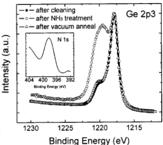
To study both the cleaning and surface nitridation effects on Ge substrates before HfO2 deposition, the Ge 2 p3 core-level XPS spectra are characterized and shown in Fig. 1. The line with closed boxes is the signal of the Ge sample共sample A兲 right after the cleaning. The main peak located at 1217.8 eV is attributed to metallic Ge 2 p3 spectrum from the sub-strate. The shoulder, ranging from 1219 to 1221 eV, is attrib-uted to GeOx (x⭐2) bonds,8 which is believed to be intro-duced during sample transportation. The circle-dotted line, as shown in Fig. 1, is the signal of the Ge sample 共sample B兲 annealed in NH3共10 min兲 after the same cleaning procedure.
It is observed that the small shoulder in sample A has evolved to a broad peak 共⬃1219.5 eV兲. Considering all the possible bonds that the Ge atoms may have, it is reasonable to infer that the broad peak consists of two types of Ge bonds: the Ge-O 共1220.1 eV兲 and Ge-N 共1218.9 eV兲. De-tailed curve fitting was carried out with Shirley background and Gaussian-Lorentzian lines 共not shown here兲. A Chi square of 4.151 is obtained, and the fitting result verifies that the whole Ge 2 p3 signal consists of three peaks which are identified as metallic Ge 共1217.8 eV兲, Ge-N bond 共1218.9 eV兲, and Ge-O bond 共1220.1 eV兲, respectively.8 The nitro-gen existence is also confirmed by the N 1s spectrum共inset of Fig. 1兲. The concentrations of oxygen and nitrogen were quantified by integrating each peak area and subtracting the background, and a layer of GeO0.83N0.17 is found on top of the Ge substrate after surface nitridation. To clarify the oxy-gen source in the GeO0.83N0.17 during the NH3 annealing, one more sample共sample C兲 was put in the NH3 treatment
chamber under same temperature without NH3 flow for 10
min after the same cleaning procedure. The XPS result is also shown in Fig. 1 with the empty-triangle line. It clearly shows that, comparing to sample A, there is no substantial oxidation in the sample C. This means that the oxygen de-tected in the GeO0.83N0.17of sample B is likely introduced by
a NH3 gas source, even though the NH3 gas purity is
99.999% 共with the main impurities of O2, H2O, and H2).
This high oxygen concentration in GeON after surface
nitri-dation implies that Ge is easier to be oxidized than nitrified. To investigate the effect of surface nitridation on the following deposited HfO2, XPS spectra of Ge 2 p3 and Hf
4 f for HfO2 deposited on germanium with and without
sur-face NH3 annealing共30 s兲 are shown in Fig. 2. For
compari-son, the XPS spectrum of Hf 4 f peak for HfO2 deposited on Si with PDA is also plotted in Fig. 2. No substantial binding energy difference is observed in Hf 4 f peaks between the Si and Ge substrates. On the other hand, Ge 2 p3 peaks at 1220.1 eV were detected and are identified as Ge-O bonds for both of the Ge samples with and without surface nitrida-tion. Since there are no metallic Ge bonds found in these signals, the Ge signals are believed to be from the as-deposited HfO2, which implies that Ge is incorporated in the
HfO2 films. This Ge incorporation phenomenon may result
from the Ge diffusion from substrate during the CVD depo-sition process 共⬃400 °C兲. Further, since no Ge-Hf bond is detected in both samples, the dielectrics are of good electri-cal insulating property in terms of chemielectri-cal states. Consid-ering the chemical similarities between Ge and Si,9 two kinds of possible structures may exist for the Ge incorpo-rated HfO2 film. The first is that the dielectric film could be
a mixture of HfO2 and GeO2. Another is that the film is
hafnium germinate and the Hf 4 f bonding is not affected by the vicinity of the Ge atom. However, this cannot be ad-dressed by analyzing the O 1s signal in this experiment be-cause it overlaps with the Ge LMM Auger signal.
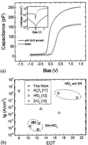
Figure 3共a兲 shows the C-V characteristics of the HfO2
Ge MOS capacitor (area⫽100m⫻100m, sweeping from inversion to accumulation兲 with surface nitridation, and its J-V curve is plotted as inset. For comparison, both C-V and J-V characteristics of the HfO2Ge MOS capacitor with-out surface nitridation 共same dimension兲 are also included. By fitting the C-V data in a computer while taking into ac-count the quantum confinement effects, it is shown that a small EOT of 10.5 Å and a low leakage current of 5.02 ⫻10⫺5 A/cm2 at V
g⫽1 V can be achieved for the MOS ca-pacitor with surface nitridation. While for the MOS caca-pacitor without surface nitridation, an EOT of 16.8 Å is obtained with a leakage current of 1.01 A/cm2at Vg⫽1 V. Figure 3共b兲 shows the gate leakage current density as a function of EOT together with published data.4 – 6Thus, though the Ge incor-poration in HfO2films is observed for both samples with and
FIG. 1. Ex situ XPS analysis of the NH3annealing effect on the Ge
sub-strates with the Ge 2 p3 spectra. The inset is the N 1s signal from the sample after NH3annealing. GeON is formed on the germanium surface.
FIG. 2. High-resolution XPS spectra of Hf 4 f and Ge 2 p3 for HfO2
depos-ited on Ge substrates. Normal position of the Hf 4 f signal implies chemi-cally good quality of the film. Ge was detected to be incorporated in the as-deposited films.
3742 Appl. Phys. Lett., Vol. 84, No. 19, 10 May 2004 Wuet al.
This article is copyrighted as indicated in the article. Reuse of AIP content is subject to the terms at: http://scitation.aip.org/termsconditions. Downloaded to IP: 140.113.38.11 On: Thu, 01 May 2014 04:24:08
without surface nitridation, and both samples show similar chemical states, the NH3 annealing is very effective in
im-proving the electrical properties of Ge MOS capacitors. The smaller EOT of the MOS capacitor with NH3annealing may
indicate a smaller thickness of the dielectric and/or the inter-facial layer than the capacitor without NH3 annealing.
How-ever, the leakage current result is different from high-MOS capacitors on silicon substrates where a larger dielectric/ interfacial layer usually yields a smaller gate leakage current. Considering together the fact that there is no significant chemical bonding difference in the dielectrics of both samples, the large difference of the leakage currents could be likely attributed to the interfacial layer. Therefore, the large leakage current of the Ge MOS capacitor implies the poor quality of interfacial layer (GeOx) when there is no surface nitridation. Regarding the work function of TaN,10the device without NH3anneal has a closer flatband voltage to the ideal one than the device with surface nitridation. The negative shift of the flatband voltage of the surface nitridation device may be due to significant positive charge (⬃5.3⫻1012 cm⫺2) introduced by the NH3 annealing.
HR-XTEM image of the Ge MOS capacitor with NH3
anneal is presented in Fig. 4共a兲. The dielectric thickness mea-sured from the TEM picture is ⬃51 Å and the dielectric constant of dielectric is ⬃18.9. From Fig. 4共a兲, it is also noticed that, unlike the interfacial layer on the Si substrate,11 the interfacial layer on Ge substrate is crystallized. The
crys-tallized interfacial layer may be related to its high oxygen concentration, since GeO2induced by gaseous O2 on the Ge
substrate was found to be polycrystalline.12 It is also noted from the TEM picture that the dielectric film has recrystal-lized, which implies that the crystallization temperature of the HfO2film with Ge is lower than 600 °C. For comparison,
the TEM image of the MOS stack without a NH3 anneal is
also presented in Fig. 4共b兲. A nonuniform interfacial layer is observed between the dielectric and the substrate. This could be due to the nonuniform oxidation behavior of the germanium,12 which degrades the MOS leakage current.
In summary, the surface NH3 annealing effects on the
physical and electrical properties of MOCVD HfO2Ge MOS
capacitors have been investigated. It is found that GeON is formed during surface nitridation (NH3 annealing兲.
Germa-nium is found to be incorporated within CVD HfO2films, in
addition, the electrical characteristics of HfO2 Ge MOS
ca-pacitors show that surface nitridation is very effective to im-prove the electrical properties in terms of Ig and EOT.
This work was supported by the Singapore ASTAR Grant No. R-263-000-267-305.
1 A. L. P. Rotondaro, M. R. Visokay, J. J. Chambers, A. Shanware, R.
Khamankar, H. Bu, R. T. Laaksonen, L. Tsung, M. Douglas, R. Kuan, M. J. Bevan, T. Grider, J. McPherson, and L. Colombo, VLSI Tech. Dig.
2002, 148共2002兲.
2J. J. Rosenberg and S. C. Martin, IEEE Electron Device Lett. 12, 639 共1988兲.
3H. Shang, H. Okorn-Schmidt, K. K. Chan, M. Copel, J. A. Ott, P. M.
Kozlowski, S. E. Steen, S. A. Cordes, H.-S. P. Wong, E. C. Jones, and W. E. Haensch, Tech. Dig.-Int. Electron Devices Meet. 2002, 441共2002兲.
4C. O. Chui, H. Kim, D. Chi, B. B. Triplett, P. C. McIntyre, and K. C.
Saraswat, Tech. Dig.-Int. Electron Devices Meet. 2002, 437共2002兲.
5
C. H. Huang, M. Y. Yang, A. Chin, W. J. Chen, C. X. Zhu, B. J. Cho, M. F. Li, and D. L. Kwong, VLSI Tech. Dig. 2003, 119共2003兲.
6W. P. Bai, N. Lu, J. Liu, A. Ramirez, D. L. Kwong, D. Wristers, A.
Ritenour, L. Lee, and D. Antoniadis, VLSI Tech. Dig. 2003, 121共2003兲.
7T. Akane, H. Okumura, J. Tanaka, and S. Matsumoto, Thin Solid Films 294, 153共1997兲.
8NIST X-ray Photoelectron Spectroscopy Database, NIST Standard
Refer-ence Database 20, Version 3.3共Web Version兲.
9G. D. Wilk, R. M. Wallace, and J. M. Anthony, J. Appl. Phys. 87, 484 共2000兲.
10
C. Ren, H. Y. Yu, J. F. Kang, Y. T. Hou, D. S. H. Chan, M.-F. Li, W. D. Wang, and D.-L. Kwong, IEEE Electron Device Lett. 25, 123共2004兲.
11H. Y. Yu, N. Wu, M. F. Li, C. X. Zhu, B. J. Cho, D.-L. Kwong, C. H.
Tung, J. S. Pan, J. W. Chai, W. D. Wang, D. Z. Chi, C. H. Ang, J. Z. Zheng, and S. Ramanathan, Appl. Phys. Lett. 81, 3618共2002兲.
12F. L. Edelman, L. N. Alexandrov, L. I. Fedina, and V. S. Latuta, Thin Solid
Films 34, 107共1976兲.
FIG. 4. HR-XTEM of the MOS structure of TaN/MOCVD HfO2/Ge共a兲
with and共b兲 without surface NH3annealing.
FIG. 3.共a兲 C – V curves were measured at a frequency of 100 kHz and J – V curves were plotted as inset. 共b兲 Gate leakage currents at Vg⫽1 V with respect to different EOTs were plotted together with published data.
3743
Appl. Phys. Lett., Vol. 84, No. 19, 10 May 2004 Wuet al.
This article is copyrighted as indicated in the article. Reuse of AIP content is subject to the terms at: http://scitation.aip.org/termsconditions. Downloaded to IP: 140.113.38.11 On: Thu, 01 May 2014 04:24:08