國 立 交 通 大 學
電子工程學系 電子研究所碩士班
碩 士 論 文
應變矽 CMOS 元件中隨機摻雜與隨機界面缺陷
引起的臨界電壓變異度研究
The Random Dopants and Random Traps Induced
Threshold Voltage Variations in Strained CMOS
Devices
研 究 生 :程政穎
指導教授 :莊紹勳 博士
中華民國 九十九 年 九 月
應變矽 CMOS 元件中隨機摻雜與隨機界面缺陷
引起的臨界電壓變異度研究
The Random Dopants and Random Traps Induced
Threshold Voltage Variations in Strained CMOS Devices
研 究 生 : 程政穎 Student : Cheng-Ying Cheng
指導教授 : 莊紹勳 博士 Advisor : Dr. Steve S. Chung
國立交通大學
電子工程學系 電子研究所碩士班
碩士論文
A Thesis
Submitted to Department of Electronics Engineering & Institute
of Electronics College of Electrical Engineering and Computer
Science
National Chiao Tung University
in Partial Fulfillment of the Requirements
for the Degree of Master of Science
in Electronics Engineering
September 2010
Hsinchu, Taiwan, Republic of China.
i
應變矽 CMOS 元件中隨機摻雜與隨機界面缺陷
引起的臨界電壓變異度研究
學生:程政穎 指導教授:莊紹勳博士
國立交通大學電子工程學系電子研究所碩士班
摘要
90 奈米及以下的 CMOS 技術,採用應變矽技術得以延續摩耳定
律
(Moore’s Law),以提昇元件性能。近年的研究中顯示在 n 型
MOSFET 元件,SiC 在 S/D 的結構提供了高的驅動電流。而在 p 型
MOSFET 元件中,單軸的應變結構 SiGe 在 S/D 及嵌入式擴散阻擋層
(EDB),有著良好的可靠度和效能。然而隨著 CMOS 元件微縮到奈米
尺度,對於前瞻 CMOS 技術而言,如何降低臨界電壓變異度(V
thvariation)成為一項重要的議題。而隨機摻雜擾動 (Random Dopant
Fluctuation, RDF)被認為是臨界電壓變異度的主要原因。此外,由製
程技術所產生的隨機界面缺陷擾動(Random Interface Trap Fluctuation,
RTF)亦會增加臨界電壓變異度。
本論文中,我們利用可將由隨機摻雜擾動引致臨界電壓變異度正
則化(Normalization)的 Takeuchi plot 來分析應變矽元件的變異度。首
先,我們解釋了應變矽元件可改善臨界電壓變異度的原因,並藉由溫
度、汲極電壓和基板電壓等效應來驗證應變矽元件擁有較佳的變異
ii
度。此外,stress 之後所造成的隨機界面缺陷導致臨界電壓變異度的
增加亦可利用 Takeuchi plot 來分析。實驗結果顯示,退化的 B
VT與界
面缺陷的數目呈比例關係。然而,在應變矽 n 型 MOSFET 元件中,
由於反轉層電子與界面缺陷的距離較近,使得庫倫散射(Coulomb
scattering)變得較強導致臨界電壓變異度退化的較嚴重。對應變矽 p
型 MOSFET 元件而言,退化的臨界電壓變異度即與應變效應無關。
iii
The Random Dopants and Random Traps Induced
Threshold Voltage Variations in Strained CMOS Devices
Student:Cheng-Ying Cheng Advisor:Dr. Steve S. Chun
g
Department of Electronics Engineering & Institute of Electronics
National Chiao Tung University
ABSTRACT
For the CMOS device technology with gate length 90 nm and beyond, strained technique has been a successful technology to extend the Moore’s law with further device scaling. Recent studies have revealed that the most mature CMOS technology is by the use of different strain techniques for n-MOSFET and p-MOSFET respectively. The use of SiC in the source and drain structure shows high driving current ability for n-MOSFET device. For p-MOSFET device, uniaxial structure with SiGe on source and drain with EDB (embedded diffusion barrier) seems to be promising in terms of its performance and reliability. However, as CMOS devices are scaled to the nanoscale dimension, reducing Vth variation becomes a significant issue
for advanced CMOS technology. Random dopant fluctuation (RDF) is the major source of Vth variation in scaled bulk CMOS. Furthermore, stress-induced random
traps fluctuation (RTF) is also considered to be another source of the enhanced Vth
variation after the hot carrier stress.
In this thesis, the variability of strained devices has been reported. The random dopant fluctuation induced Vth variation can be normalized by Takeuchi plot. First,
iv
the reasons for Vth variation improvement of strained devices are analyzed. The
factors affecting the Vth variation which include temperature, drain bias, and substrate
bias are examined. Experimental results show better variability of strained devices. Secondly, the basis of the enhanced Vth variation caused by stress-induced random
traps can still follow the Takeuchi plot. The results show that the aggravated BVT is
proportional to the number of interface traps. However, for strained n-MOSFETs, due to the closer distance between inversion layer electrons and interface traps, Coulomb scattering limited by interface traps becomes strongly enhanced which results in a faster aggravation of Vth variation. For strained p-MOSFETs, the aggravated Vth
v
Acknowledgements
兩年的實驗室生活是精采豐富的,但同時也充滿艱辛與汗水。首先要感謝 的是我的指導教授:莊紹勳教授,老師給予的生活上與專業上的指導與建議,讓 我在學業上與研究上獲益良多並學習到對事物應有的嚴謹態度以及處理方法。除 此之外,對於課業外的生活技能、觀念的督促,讓我必頇在此表達感謝之意。 感謝在兩年研究生涯中,與我一起嚐遍酸甜苦辣的同學,包括永涵、元宏 與士嵩,我們一起經歷困苦的研究過程,相信數年後再聚首,一定倍感溫馨。對 於汪老師研究群的同學,即使我們身在不同的研究群,但我們的感情就像是一家 人一樣,希望以後在業界相遇時還能保有我們現在的真誠,也祝福小馬、佑亮與 榮標學長能夠順利取得博士學位,此外也感謝承翰、書民與嘉偉,感謝有你們這 群學弟平日對於實驗室的付出,使學長們能夠專心於研究上,在此,輕遞一份真 摯的祝福,希望明年亦能看見你們順順利利的畢業。 另外,在此也要感謝聯華電子在測試元件和技術上的協助,使本研究得以順 利完成。 最後,要感謝我的家人與女友湘怡,你們是我最大的精神支柱,有了你們的 支持和鼓勵,使我能堅持到現在。 謹將這份榮耀獻給培養我多年的父母親。vi
Contents
Chinese Abstract……….i English Abstract………iii Acknowledgments………v Contents………vi Figure Captions...viiiChapter 1 Introduction
...1 1.1 Background...11.2 The Motivation of this Work...2
1.3 Organization of the Thesis...2
Chapter 2 Experimental Setup and V
thVariation
………..52.1 Introduction...5
2.2 Experimental Setup...6
2.3 Theory of Takeuchi Plot...6
Chapter 3 Variability of Strained n-MOSFETs
………...143.1 Introduction...14
3.2 Device Preparation...15
3.3 Performance of Strained n-MOSFETs...15
3.4 Variability of Strained n-MOSFETs...15
3.5 Factors Affecting the Vth Variation...16
3.5.1 Effect of the Temperature...16
3.5.2 Effect of the Drain Bias...17
3.5.3 Effect of the Substrate Bias...17
3.5.4 Discussion of the Bias Effect...18
3.6 Impact of Stress-induced Random Interface Traps...18
3.6.1 Introduction...18
3.6.2 Charge Pumping Measurement...19
3.6.3 Variability after FN Stress...19
3.6.4 Variability after PBTI Stress...20
3.6.5 Discussion...20
Chapter 4 Variability of Strained p-MOSFETs
...424.1 Introduction...42
vii
4.3 Performance of Strained p-MOSFETs...43
4.4 Variability of Strained p-MOSFETs...43
4.5 Factors Affecting the Vth Variation...44
4.5.1 Effect of the Temperature...44
4.5.2 Effect of the Drain Bias...45
4.5.3 Effect of the Substrate Bias...45
4.6 Impact of Stress-induced Random Interface Traps...45
4.6.1 Introduction...45
4.6.2 Variability after FN Stress...46
4.6.3 Variability after NBTI Stress...47
4.6.4 Discussion...47
Chapter 5 Summary and Conclusion
...67viii
Figure Captions
Chapter 1
Fig. 1.1 Example of random threshold voltage fluctuations. Closely located identically designed 4k transistors are measured [1.3].
Chapter 2
Fig. 2.1 The experimental setup for the current-voltage measurement of MOSFETs. Automatic controlled characterizations system is setup based on the PC controlled instrument environment.
Fig. 2.2 Measured NMOS Vth variation with (a) slope AVT and (b) slope BVT. The
slope AVT depends on Vth and Tinv while BVT does not [2.4].
Fig. 2.3 Example of Takeuchi plots for NMOS and PMOS. BVT of NMOS is larger
than that of PMOS.
Fig. 2.4 The analytical calculation and the 3D-TCAD simulation results of a Boron clustering model [2.11].
Chapter 3
Fig. 3.1 The cross-section view of the experimental devices. (a) control, (b) SiC S/D (uniaxial-strain), and (c) SiC S/D-E devices (uniaxial-strain). All of them
are <100> channel on (100) substrate.
Fig. 3.2 The Ion-Ioff characteristics of all the nMOSFET devices. SiC S/D-E device
can improve the driving current by an increment of 23% over the control (Si-bulk).
Fig. 3.3 The ID-VD curves of the splits and control. The SiC S/D-E device shows
67% ID,sat enhancement over control devices.
Fig. 3.4 A 94% electron mobility enhancement is obtained for the long SiC S/D-E device compared to the control.
ix
Fig. 3.5 Takeuchi Plots of n-MOSFETs. The slope indicates the value of BVT.
Fig. 3.6 Comparison of BVT for n-MOSFETs. BVT of SiC S/D-E shows a 26%
improvement to the control.
Fig. 3.7 Dependence of BVT on the temperature. Strained devices show no
degradation compared to the control devices.
Fig. 3.8 VDS dependence of σVth. Strained devices exhibit weak dependence of Vth
variation on the drain bias.
Fig. 3.9 Dependence of BVT on VBS. Strained devices show better BVT as substrate
bias increases.
Fig. 3.10 The schematic diagram of the depletion region profile under different bias conditions.
Fig. 3.11 The charge pumping currents of all the n-MOSFETs after FN stress. Fig. 3.12 The average interface traps of all the n-MOSFETs after FN stress. Fig. 3.13 The evolution of BVT for all the n-MOSFETs during FN stress.
Fig. 3.14 Relationship of BVT with interface traps for all the n-MOSFETs after FN
stress.
Fig. 3.15 The charge pumping currents of all the n-MOSFETs after PBTI stress. Fig. 3.16 The average interface traps of all the n-MOSFETs after PBTI stress. Fig. 3.17 The evolution of BVT for all the n-MOSFETs during PBTI stress.
Fig. 3.18 Relationship of BVT with interface traps for all the n-MOSFETs after PBTI
stress.
Fig. 3.19 The enhanced BVT caused by stress-induced interface traps during (a) FN
stress and (b) PBTI stress.
Fig. 3.20 Schematics of the valley configuration in Si and strained-Si inversion layers to illustrate the larger σVth in strained devices after the stress.
Chapter 4
x
S/D (uniaxial-strain), and (c) SiGe S/D w/ EDB devices (uniaxial-strain). All of them are <110> channel on (100) substrate.
Fig. 4.2 The Ion-Ioff characteristics of all the pMOSFET devices. SiGe S/D device
can improve the driving current by 51% over the control(Si-bulk).
Fig. 4.3 The ID-VD curves of the splits and control. The SiGe S/D device shows 38%
ID,sat enhancement over control devices.
Fig. 4.4 A 148% hole mobility enhancement is obtained for the long SiGe S/D device compared to the control.
Fig. 4.5 Takeuchi Plots of p-MOSFETs. The slope represents the value of BVT.
Fig. 4.6 Comparison of BVT for p-MOSFETs. BVT of SiGe S/D w/ EDB shows the
10% improvement to the control.
Fig. 4.7 The dependence of BVT on the temperature. Strained devices show no
degradation compared to the control device.
Fig. 4.8 VDS dependence of σVth. Strained devices exhibit weak dependence of Vth
variation on the drain bias.
Fig. 4.9 The dependence of BVT on VBS. Strained devices show better BVT as
substrate bias increases.
Fig. 4.10 The charge pumping currents of all the p-MOSFETs after FN stress. Fig. 4.11 The average interface traps of all the p-MOSFETs after FN stress. Fig. 4.12 The evolution of BVT for all the p-MOSFETs during FN stress.
Fig. 4.13 Relationship of BVT with interface traps for all the p-MOSFETs after FN
stress.
Fig. 4.14 The charge pumping currents of all the p-MOSFETs after NBTI stress. Fig. 4.15 The average interface traps of all the p-MOSFETs after NBTI stress. Fig. 4.16 The evolution of BVT for all the p-MOSFETs during NBTI stress.
Fig. 4.17 Relationship of BVT with interface traps for all the p-MOSFETs after NBTI
stress.
xi
1
Chapter 1
Introduction
1.1 Background
Moore’s Law has driven CMOS devices scaling for several decades. However, the scaling limits continue to be a great challenge. In order to properly operate today’s very large scale CMOS integrated circuits, where hundreds of millions of transistors are gathered to analyze more complex integration, it is desirable to obtain the identical characteristics or small tolerance from the target characteristics of all the manufactured MOSFETs. However, due to several reasons, it becomes a serious issue today [1.1-1.2]. One of the most significant issues is the variability induced by the increase of random fluctuation for continuing further scaling down of transistors. Random fluctuations refer to a kind of variability that exhibits no correlation between neighboring devices as shown in Fig. 1.1 [1.3]. Various sources of the MOSFETs variability such as random placement of doped impurities (random dopant fluctuation, RDF), line edge roughness, gate oxide roughness and so on. It is increased by the reduction of device size since the electrical characteristics become more sensitive to the number of dopants in the depletion region. As a result, it cannot be eliminated by simply improving the process and device design. Therefore, as CMOS devices are scaled to the nanoscale dimension, there are multiple challenges to be overcome for advanced CMOS technology.
1.2 The Motivation of This Work
2
32 nm and even beyond has been widely acknowledged as encountering many more challenges with regard to Vth variation issues. Recent study [1.4] has revealed that
random dopant fluctuation (RDF) is the major source of Vth variation in scaled bulk
CMOS. To improve the RDF, FDSOI or FinFET with undoped (lighter) channel
[1.5-1.7], has been proposed subsequently to reduce the variability effectively.
Also, recent developments [1.8] in CMOS technology have highlighted the need in using the strain technique as a method to extend the scaling of CMOS device for high speed and low power logic applications. Several approaches among them, such as process-induced stress techniques, strained SiGe channel devices, substrate engineering, and hybrid substrate technology, have been utilized to improve device performance. However, so far, the sources and the mechanisms of Vth variation have
not been experimentally clarified on strained devices. As a consequence, we are interested in understanding the variability of strained devices.
For the first time, in this thesis, we apply the Takeuchi plot [1.9], which normalizes Vth variation in terms of electrical equivalent gate dielectric thickness at
inversion Tinv and Vth, to observe the Vth variation in various n-MOSFETs and
p-MOSFETs employing different process-induced strain. The impact of their strains on the device reliability and variability will be investigated and compared.
1.3 Organization of the Thesis
There are five parts in this thesis. Chapter 1 is the introduction. We describe the motivation and organization of this thesis. In Chapter 2, we describe the experimental setup and the method of normalizing the Vth variation (Takeuchi plot) used in
3
effects of temperature, drain bias, and substrate bias of strained n-MOSFETs will be examined. Moreover, the enhanced Vth variation caused by stress-induced interface
traps was proposed. In Chapter 4, by applying similar analysis, we will discuss the variability for strained p-MOSFETs. Finally, the summary and conclusion will be included in Chapter 5.
4
Fig. 1.1 Example of random threshold voltage fluctuations. Closely located identically designed 4k transistors are measured [1.3].
5
Chapter 2
Experimental Setup and V
thVariation
2.1 Introduction
As devices are scaled to the nanoscale dimension, it is important to understand random fluctuations. Since there are many possible microscopic causes, it is desirable to understand the mechanism of variability. Therefore, electrical measurement of random fluctuations is a useful technique to observe such microscopic effects. It is necessary to collect a lot of data of σ (standard deviation) values for various kinds of transistors fabricated by different process conditions. If such data are properly compared and analyzed, it may become possible to extract quantitative information about random fluctuations. Based on this consideration, a simple normalization method for comparing σ values of random threshold voltage fluctuations was proposed. The method was used to compare devices of various origins to analyze the causes of random fluctuations [2.1].
This chapter is divided into two sections. First, we will illustrate the fundamental experimental setup to characterizing CMOS devices. Second, the method of normalizing the Vth variation (Takeuchi plot) used in this thesis will be introduced,
6
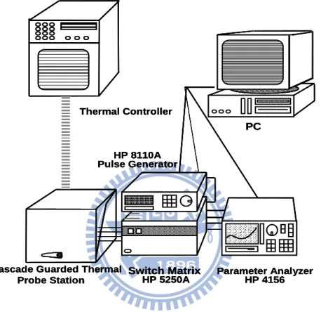
2.2 Experimental Setup
The experimental setup for the current-voltage measurement of devices is illustrated in Fig. 2.1. Based on the PC controlled instrument environment by HP-IB (GP-IB, IEEE-488 Standard) interface, the complicated and long-term characterization procedures during analyzing the behaviors in MOSFETs can be easily achieved. As shown in Fig. 2.1, the equipments, including the semiconductor parameter analyzer (HP 4156C), low leakage switch mainframe (HP E5250A), dual channel pulse generator (HP 8110A), cascade guarded thermal probe station and a
thermal controller, provides an adequate capability for measuring the device
characteristics. In addition, programs written by HT-Basic were used to execute the measurement via HP-IB interface.
2.3 Theory of Takeuchi Plot
It is well known that standard deviation of threshold voltage σVth usually
follows a relationship [2.2] VT th A V WL (2.1)
where L is channel length and W is channel width. Here, the coefficient AVT (Pelgrom
coefficient) can be taken as a normalized σVth with respect to the channel size, and is
often used for evaluating and comparing fluctuations. By using AVT, fair comparison
between FETs with different geometry is possible. However, it is not suitable for comparing different kinds of transistors, where gate oxide thickness or threshold voltage is not necessarily identical. According to a simple model [2.3], the σVth
7 dominated by RDF is expressed by 1 4 3 sub dep / th sub inv N W q V N C LW (2.2)
where Cinv = εOX/Tinv is the electrical gate capacitance per area at inversion, Nsub is the
channel impurity concentration, and Wdep is the width of the channel depletion layer.
Note that the dependence on L and W is common to (2.1) and (2.2). At the same time, the NsubWdep term is also included in the theoretical calculation of Vth as
sub dep th fb s inv qN W V V C . (2.3)
By substituting the NsubWdep term in (2.3) into (2.2), we can derive
3 3 3 3 sub dep th inv th fb s inv th fb s inv ox inv th O inv th O VT ox N W q V C LW q(V V ) q T (V V ) LWC LW T (V V ) T (V V ) q B LW LW (2.4)
where Tinv is the electrical gate oxide thickness at inversion, and VO is defined as
0 1
O fb s
V V . V. (2.5)
8
Equation (2.4) indicates that σVth is proportional to T (Vinv thV ) / LWO . In the
Takeuchi plot, σVth is normalized by T (Vinv thV ) / LWO . Here, Tinv, Vth , VO, L
and W are the median values of the devices.
As an example, the measured data for σVth are plotted in Fig. 2.2(a). The slope
AVT is a conventional index of Vth variation and depends on Vth and Tinv. The
measurement of σVth is also plotted with a different x-axis as shown in Fig. 2.2(b),
where the slope is defined as BVT [2.4]. The slope is an indicator of Vth variation. It is
found that BVT remains constant with varying Vth and Tinv. It is due to Vth variation
normalized in terms of Tinv and Vth. Therefore, BVT is a useflu tool to investigate the
origins of Vth variation.
Moreover, when Vth variation is dominated solely by RDF, the analytically
calculated BVT equals q/3ox (about 1.2). Since the analytical calculation does not
take the effect of the discreteness of the channel dopant on the channel surface direction into account, it underestimates BVT. According to the 3-D technology
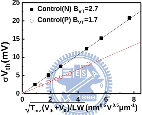
computer-aided design (3-D-TCAD) calculation, which takes the discreteness of the channel dopant fully into account, BVT of RDF is 1.5 [2.1]. In Fig. 2.3, BVT of PMOS
is 1.7 and close to that of RDF (which is 1.5). This result indicates that the Vth
variation of PMOS is dominated by RDF [2.5-2.9]. BVT of NMOS is 2.7 and larger
than that of RDF (which is 1.5). This result indicates that Vth variation of NMOS is
dominated not only by RDF but also by other factors.
To explain the larger BVT of NMOS, a Boron clustering model is proposed. In
general, it is well known that Boron atoms with high concentration are clustered in Si
[2.10]. Some Boron atoms of channel dopants gather with weak binding force and act as one Boron cluster. In this case, the charge of a carrier q is replaced with nq and
9
NSUB is replaced with NSUB/n. Vth is not changed by these replacements, i.e.,
2 6 2 6 sub dep th fb s inv sub dep th fb s inv ( . a) ( . b) qN W V V C (nq)(N / n)W and V V . C
σVth increases by a factor of n , i.e.,
2 7 2 7 3 3 3 sub dep th inv
sub dep sub dep
th inv inv ( . a) ( . b) N W q V C LW (N / n)W N W nq q V n . C LW C LW
As a result, BVT increases by a factor of n , i.e.,
3 ox 3 ox
q nq
. (2.8)
Fig. 2.4 shows the relationship between BVT and the number of clustering Boron
atoms, n, calculated by the analytical and 3-D-TCAD calculation [2.11]. On the basis of the 3-D-TCAD calculation and measured BVT of 2.7, actual BVT can be explained
10 HP 8110A Pulse Generator
Cascade Guarded Thermal Probe Station Switch Matrix HP 5250A Parameter Analyzer HP 4156 PC Thermal Controller
Fig. 2.1 The experimental setup and environment for basic I-V measurement of MOSFET’s.
HP 8110A Pulse Generator
Cascade Guarded Thermal Probe Station Switch Matrix HP 5250A Parameter Analyzer HP 4156 PC Thermal Controller HP 8110A Pulse Generator
Cascade Guarded Thermal Probe Station Switch Matrix HP 5250A Parameter Analyzer HP 4156 PC Thermal Controller
Fig. 2.1 The experimental setup and environment for basic I-V measurement of MOSFET’s.
Fig. 2.1 The experimental setup for the current-voltage measurement of MOSFETs. Automatic controlled characterizations system is setup based on the PC controlled instrument environment.
11
(a)
(b)
Fig. 2.2 Measured NMOS Vth variation with (a) slope AVT and (b) slope BVT. The
slope AVT depends on Vth and Tinv while BVT does not [2.4].
12
Fig. 2.3 Example of Takeuchi plots for NMOS and PMOS. BVT of NMOS is larger
than that of PMOS.
0
2
4
6
8
0
5
10
15
20
25
V
th
(m
V
)
0.5 0.5 -1 inv th 0T (V +V )/LW (nm
V
μm )
Control(N) B
VT=2.7
Control(P) B
VT=1.7
13
Fig. 2.4 The analytical calculation and the 3D-TCAD simulation results of a Boron clustering model [2.11].
14
Chapter 3
The Variability of Strained n-MOSFETs
3.1 Introduction
Recently, researches have shown an increasing interest in the strain technology. Strained silicon technology is essential for the continuation of the scaling in MOSFET devices, owing to its high impact on carrier mobility and thus on drive current improvement [3.1]. When applied to the direction of the channel, tensile strain improves the performance of n-MOSFET devices, while compressive strain is beneficial for p-MOSFET devices. The local strain, such as capping layer, SiGe on S/D, and SiC on S/D are induced by the process. They are usually uniaxial strain. Compared to the global strain usually biaxial strain, the local strain has less dislocation issues.
However, as the devices are scaled, a variety of process-induced variations become more obvious. One of the most critical issues is Vth variation. Random
dopants in the channel and source/drain regions are the dominant source of Vth
variation in scaled bulk CMOS. It already profoundly affects the SRAM design [3.2]
and, in logic circuits, causes statistical timing problems [3.3]. In both cases, statistical variability restricts threshold and supply voltage scaling, causing static and dynamic power dissipation problems [3.4].
In this chapter, we will demonstrate Vth variation which can be suppressed by
advanced strained-Si technology meanwhile the performance of devices keeps improved for n-MOSFETS. Extensive comparisons between strained and control
15
n-MOSFETs will be justified on examining the effects of temperature, drain bias, and substrate bias. In addition, the impact of stress-induced random interface traps fluctuation (RIF) on the device variability will also be verified.
3.2 Device Preparation
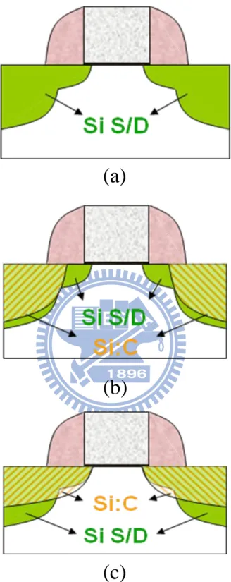
The devices were fabricated by the advanced 40nm CMOS technology at UMC. The schematic cross section diagram of n-MOSFET splits is shown in Fig. 3-1. In this figure, Fig. 3-1(a) is the control device, Fig. 3-1(b) is the SiC on S/D device (uniaxial-strain) and Fig. 3-1(c) is the SiC on S/D-E device (uniaxial-strain). Both n-MOSFETs are <100> channel on (100) substrate. All these test devices have 12Å EOT gate oxide with SiON process. Devices with various areas were measured for Takeuchi plots. The device threshold voltage was measured by the extrapolation and constant current method.
3.3 Performance of Strained n-MOSFETs
In Fig. 3.2, the Ion-Ioff curve of the SiC S/D-Edevices show 23.6% current gain
over the control (bulk-Si) and 13% improvement for typical SiC S/D devices. Moreover, Fig. 3.3 shows 67% enhancement of ID,sat for the SiC S/D-E devices over
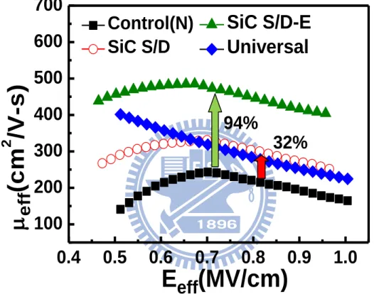
the control. As shown in Fig. 3.4, the peak mobility of the SiC S/D-E devices exhibits a 94% increase in comparison to the control.
3.4 Variability of Strained n-MOSFETs
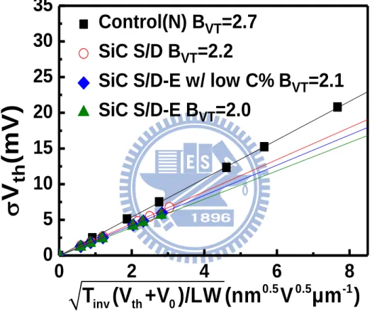
Figure 3.5 shows the Takeuchi plot of the n-MOSFET splits, in which the BVT of
16
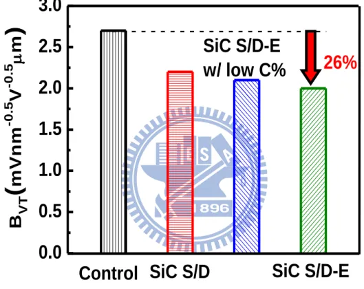
reduction of 26% to the control in Fig. 3.6. To explain the smaller BVT of strained
devices, we consider that the strain effect could reduce the number of clustering Boron atoms by using Boron clustering model [3.5]. In addition, the Carbon diffuses out to the vicinity of S/D junction and substrate region is also capable of describing the suppression of Vth variation. The diffusion of interstitial diffuser species such as
Boron through annihilation of interstitials (Boron TED) will be reduced by the Carbon, resulting in decreasing Vth variation [3.6-3.7]. In other words, as the stressors (Carbon)
diffuse out to the vicinity of S/D junction and channel region, the effective dopant concentration is decreased, and Vth fluctuation is improved. Moreover, the SiC S/D
and SiC S/D-E with low C% have larger BVT than that of SiC S/D-E due to less
channel strain effect [3.8]. Therefore, the more the strain in channel is, the smaller the BVT of device becomes.
3.5 Factors Affecting the V
thVariation
3.5.1 Effect of the Temperature
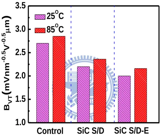
To understand the effect of the temperature on strained n-MOSFETs, devices are measured at elevated temperature (85OC). It was found that BVT is larger at 85OC in
Fig. 3.7 for all the n-MOSFET device splits. As the temperature increases, the thermal fluctuation of the lattice becomes larger. The carrier moving through the crystal is easier to be scattered by a vibration of the lattice results in enhanced BVT. Moreover, a
higher leakage current of device at elevated temperature is also a source of increasing BVT, i.e., g th ds q(V V ) / mkT qV / kT 2 ds eff ox W kT I C (m 1)( ) e (1 e ) L q (3.1)
17
where m is the body effect coefficient [3.9]. Therefore, the Vth variation is increased
as the device is heated. Also, the result shows the amount of enhanced BVT of SiC S/D
and SiC S/D-E is similar to that of control which exhibits no degradation compared to the control.
3.5.2 Effect of the Drain Bias
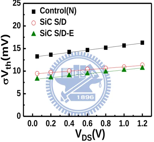
The effect of the drain bias (VDS) on Vth variation was also examined. Fig. 3.8
shows the Vth variation increases with increasing drain bias. This is because the
depletion region around the drain junction becomes wider as the drain bias increases such that more ionized impurities are produced. SiC S/D and SiC S/D-E exhibit weak dependence of Vth variation on the drain bias as a result of the strain effect. Because
there are less Boron atoms clustered in strained-Si, the effect of RDF becomes minor. It indicates good SCE immunity (small DIBL) and this immunity is a primary requirement for small variability because devices are operated at high drain bias.
3.5.3 Effect of the Substrate Bias
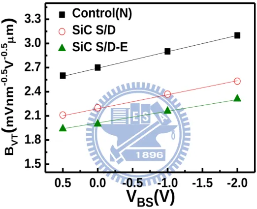
Dependence of BVT on substrate bias (VBS) is shown in Fig. 3.9. BVT increases as
substrate bias increases. It is well known that ionized impurities in depletion region are the major source of Vth variation. By applying substrate bias, more ionized
impurities are produced since the bulk depletion width becomes wider results in enhanced BVT. Also, based on the same reasoning as that in section 3.4.2, SiC S/D and
SiC S/D-E show better BVT as substrate bias increases due to the strain effect which
18 3.5.4 Discussion of the Bias Effect
Figure 3.10 shows the variances in depletion width under different bias conditions. It is well known that the depletion width increases with increasing bias. Moreover, random ionized impurities in the depletion region are the dominant source of Vth variation. As substrate concentration is increased, RDF becomes more serious
since Vth variation is proportional to Nsub1/4 as derived in section 2.3, i.e.,
1 4 3 sub dep / th sub inv N W q V N . C LW (3.2)
Therefore, it is expectable that the effects of drain and substrate bias become more dramatic as the substrate concentration is increased.
3.6 Impact of Stress-induced Random Interface traps
3.6.1 Introduction
A large number of variation effects of both types have been revealed in many studies. Examples include: random dopant fluctuation (RDF) [3.10], line-edge roughness (LER) [3.11-3.12], and local oxide thickness variations [3.13]. In addition to these effects, recent study [3.14] has proved that process-induced random interface traps fluctuation (RIF) are required for proper interpretation of Vth variation in CMOS
technologies. However, so far, none has been reported on the effect of stress-induced random interface traps. Thus, in this section, we will discuss the device variability after FN and PBTI stresses.
19 3.6.2 Charge Pumping Measurement
The charge pumping (CP) measurement is efficient for the reliability characterization. However, the charge pumping measurement can’t be used reliably in the small size devices due to the small charge pumping current and the gate leakage current. Recently, a low leakage Incremental Frequency Charge Pumping (IFCP) measurement for CMOS devices has been developed [3.15] to get more reliable results. Since charge pumping current is proportional to the generated interface traps, we use IFCP to evaluate the interface traps for the stressed devices.
3.6.3 Variability After FN Stress
Figure 3.11 shows the measured ICP for studying the vertical field effect using
FN stress (VGS-Vth= 2V for 300sec). It is observed that the ICP of SiC S/D-E is larger
than the others which could be attributed to the Carbon out-diffusion [3.16] and the ICP of SiC S/D is the smallest one which exhibits better reliability. The average
interface traps generation among these three devices during stress time, from 100sec to 500sec, is shown in Fig. 3.12. The number of interface traps increases with increasing stress time. Since the positions and number of charges trapped at the SiO2/Si interface randomly vary, it is possible for this variation to affect the Vth
variation [3.17]. Thus, the comparison of BVT during stress time is shown in Fig. 3.13
to verify the possibility. Also, Fig. 3.14 shows the relationship of BVT with interface
traps. It is obvious that BVT is aggravated after FN stress. Moreover, the aggravated
BVT is proportional to interface traps. This result indicates that stress-induced
20 3.6.4 Variability After PBTI Stress
By applying similar analysis, we apply the PBTI stress (VGS-Vth= 2V at 85℃) to
produce the interface traps at the SiO2/Si interface which would show a more
aggravated BVT. Fig. 3.15 shows the measured ICP after PBTI stress (VGS-Vth= 2V for
300sec, at 85℃). Based on the same reasoning as described in 3.5.3, the ICP of SiC
S/D-E is larger than the others. In addition, the ICP of all n-MOSFET splits after PBTI
stress are larger than that of FN stress. It indicates that more interface traps are produced after PBTI stress as shown in Fig. 3.16. Fig. 3.17 shows the comparison of BVT during stress time. Fig. 3.18 shows the relationship of BVT with interface traps.
We observe a more aggravated BVT after PBTI stress which is attributed to the more
interface traps generation, but the aggravated BVT is also proportional to interface
traps.
3.6.5 Discussion
Figure 3.19(a)-(b) show the enhanced BVT during FN and PBTI stress. The
results give us a more specific evidence to confirm the interface traps which results from the FN and PBTI stress would enhance Vth variation, i.e. σ(Vth)2 = σ(dopant)2 +
σ(Nit)2. In addition, this result shows that the control of the interface quality in SiC
S/D and SiC S/D-E is very important and even more than in control devices.
It was also found that the amount of enhanced BVT is larger in strained devices.
The distance between inversion layer electrons and interface traps located at the SiO2/Si interface can be a key parameter to explain the impact of strain on the
enhanced BVT. Fig. 3.20 schematically shows the electron distributions in the Δ2 and
21
scattering centers [3.18]. It is well known that in strained-Si, most electrons are in the twofold valleys (Δ2) where the electron distribution is more confined near the interface than in the fourfold valleys (Δ4). Thus, the Coulomb scattering limited by interface traps becomes strong causing a great impact on enhanced Vth variation.
22
(a)
(b)
(c)
Fig. 3.1 The cross-section view of the experimental devices. (a) control, (b) SiC S/D (uniaxial-strain), and (c) SiC S/D-E devices (uniaxial-strain). All of them
23
Fig. 3.2 The Ion-Ioff characteristics of all the nMOSFET devices. SiC S/D-E device
can improve the driving current by an increment of 23% over the control (Si-bulk).
1000
1200
1400
1600
1E-8
1E-7
1E-6
Control(N)
SiC S/D
SiC S/D-E
I
off(A
/u
m
)
I
on
(uA/um)
nMOSFETs
13.5%
10.1%
24
Fig. 3.3 The ID-VD curves of the splits and control. The SiC S/D-E device shows 67%
ID,sat enhancement over control devices.
0.0
0.2
0.4
0.6
0.8
1.0
0
4
8
12
16
20
I
D
(m
A
)
V
D
(V)
Control(N)
SiC S/D
SiC S/D-E
V
G-V
th=1V
27%
67%
25
Fig. 3.4 A 94% electron mobility enhancement is obtained for the long SiC S/D-E device compared to the control.
0.4
0.5
0.6
0.7
0.8
0.9
1.0
100
200
300
400
500
600
700
SiC S/D-E
Universal
e
ff
(cm
2/V
-s
)
E
eff
(MV/cm)
Control(N)
SiC S/D
94%
32%
26
Fig. 3.5 Takeuchi Plots of n-MOSFETs. The slope indicates the value of BVT.
0
2
4
6
8
0
5
10
15
20
25
30
35
V
th
(m
V
)
0.5 0.5 -1 inv th 0T (V +V )/LW (nm V
μm )
Control(N) B
VT
=2.7
SiC S/D B
VT
=2.2
SiC S/D-E w/ low C% B
VT
=2.1
SiC S/D-E B
VT
=2.0
27
Fig. 3.6 Comparison of BVT for n-MOSFETs. BVT of SiC S/D-E shows a 26%
improvement to the control.
0.0
0.5
1.0
1.5
2.0
2.5
3.0
B
VT(
m
V
n
m
-0 .5V
-0 .5
m
)
Control SiC S/D
SiC S/D-E
w/ low C%
SiC S/D-E
26%
28
Fig. 3.7 Dependence of BVT on the temperature. Strained devices show no
degradation compared to control devices.
1.0
1.5
2.0
2.5
3.0
3.5
B
VT(
m
V
n
m
-0 .5V
-0 .5
m
)
SiC S/D-E
SiC S/D
25
OC
85
OC
Control
29
Fig. 3.8 VDS dependence of σVth. Strained devices exhibit weak dependence of Vth
variation on the drain bias.
0.0 0.2 0.4 0.6 0.8 1.0 1.2
0
5
10
15
20
25
V
DS
(V)
V
th
(m
V
)
Control(N)
SiC S/D
SiC S/D-E
30
Fig. 3.9 Dependence of BVT on VBS. Strained devices show better BVT as substrate
bias increases.
0.5
0.0
-0.5
-1.0
-1.5
-2.0
1.5
1.8
2.1
2.4
2.7
3.0
3.3
B
VT(
m
V
n
m
-0 .5V
-0 .5
m
)
V
BS
(V)
Control(N)
SiC S/D
SiC S/D-E
31
Fig. 3.10 Schematic diagram of the depletion region profile under different bias conditions.
32
Fig. 3.11 The charge pumping currents of all the n-MOSFETs after FN stress.
-1.0
-0.5
0.0
0.5
1.0
0
50
100
150
200
250
300
350
400
V
gh
(V)
I
cp
@
1
M
H
z
(p
A
)
FN stress@25
OC
V
G
-V
th
=2V,300sec
Control(N)
SiC S/D
SiC S/D-E
33
Fig. 3.12 The average interface traps of all the n-MOSFETs after FN stress.
1
2
3
4
5
6
N
it
(x10
10
/c
m
2
)
Stress Time(x100sec)
FN stress@25
OC,V
G
-V
th
=2V
Control(N)
SiC S/D
SiC S/D-E
2
3
4 5
34
Fig. 3.13 The evolution of BVT for all the n-MOSFETs during FN stress.
1
2.0
2.4
2.8
3.2
3.6
B
VT(
m
V
n
m
-0 .5V
-0 .5
m
)
FN stress@25
OC,V
G
-V
th
=2V
Control(N)
SiC S/D
SiC S/D-E
Stress Time(x100sec)
2
3
4 5
35
Fig. 3.14 Relationship of BVT with interface traps for all the n-MOSFETs after FN
stress.
2.4
2.8
3.2
3.6
4.0
4.4
4.8
2.0
2.4
2.8
3.2
3.6
B
VT(
m
V
n
m
-0 .5V
-0 .5
m
)
FN stress@25
OC,V
G-V
th=2V
Control(N)
SiC S/D
SiC S/D-E
N
it
(x10
10
/cm
2
)
36
Fig. 3.15 The charge pumping currents of all the n-MOSFETs after PBTI stress.
-1.0
-0.5
0.0
0.5
1.0
0
100
200
300
400
500
V
gh
(V)
I
cp
@
1
M
H
z
(p
A
)
PBTI stress@85
OC
V
G-V
th=2V,300sec
Control(N)
SiC S/D
SiC S/D-E
37
Fig. 3.16 The average interface traps of all the n-MOSFETs after PBTI stress.
1
2
3
4
5
6
7
N
it
(x10
10/c
m
2)
Stress Time(x100sec)
PBTI stress@85
OC,V
G
-V
th
=2V
Control(N)
SiC S/D
SiC S/D-E
2
3
4 5
38
Fig. 3.17 The evolution of BVT for all the n-MOSFETs during PBTI stress.
1
2.0
2.4
2.8
3.2
3.6
B
VT(
m
V
n
m
-0 .5V
-0 .5
m
)
Stress Time(x100sec)
PBTI stress@85
OC,V
G-V
th=2V
Control(N)
SiC S/D
SiC S/D-E
2
3
4 5
39
Fig. 3.18 Relationship of BVT with interface traps for all the n-MOSFETs after PBTI
stress.
2
3
4
5
6
7
2.0
2.4
2.8
3.2
3.6
4.0
B
VT(
m
V
n
m
-0 .5V
-0 .5
m
)
N
it
(x10
10
/cm
2
)
PBTI stress@85
OC,V
G-V
th=2V
Control(N)
SiC S/D
SiC S/D-E
40
0
10
20
30
40
50
60
70
FN stress@25
OC
V
G-V
th=2V
Stress Time(sec)
Control(N)
SiC S/D
SiC S/D-E
B
VT
(%
)
100
300
500
(a)
(b)
Fig. 3.19 The enhanced BVT caused by stress-induced interface traps during (a) FN
stress and (b) PBTI stress.
0
10
20
30
40
50
60
70
PBTI stress@85
OC
V
G-V
th=2V
Stress Time(sec)
Control(N)
SiC S/D
SiC S/D-E
B
VT
(%
)
100
300
500
41
Fig. 3.20 Schematics of the valley configuration in Si and strained-Si inversion layers to illustrate the larger σVth in strained devices after stress.
42
Chapter 4
Variability of Strained p-MOSFETs
4.1 Introduction
Mobility enhancement is a method to improve the CMOS devices performance with the scaling of the device size. The increase of carrier mobility is necessary to realize the high-speed logic CMOS devices. Recently, various strain technologies have been utilized to enhance the drive current. It is necessary to understand the introduced uniaxial and biaxial strains in n-MOSFET or p-MOSFET devices. Initially, the typical mobility enhancement of n-type strained-Si is much larger than that of p-type devices. Several techniques have been further developed to enhance the p-MOSFET performance, i.e., SiGe on S/D device [4.1]. Materials with same crystal structure but different lattice are good candidates for the strain engineering. The SiGe has been successfully incorporated in the source and drain of p-MOSFET devices to strain the channel compressively and increase the hole mobility. However, as the devices being scaled, a variety of process-induced variations will need to be overcome. One of the most critical issues is Vth variation. We have demonstrated in previous
chapter that strained n-MOSFET with embedded SiC on source and drain could suppress variability.
In this chapter, we will demonstrate Vth variation is suppressed by advanced
strained-Si technology meanwhile the performance of devices keeps improved for p-MOSFETs. Extensive comparisons between strained and control p-MOSFETs will be justified on examining the effects of temperature, drain bias, and substrate bias. In addition, the impact of stress-induced random interface traps fluctuation (RTF) on the
43 device variability will be also verified.
4.2 Device Preparation
The devices were fabricated by the advanced 40nm CMOS technology at UMC. The schematic cross section diagram of p-MOSFET splits is shown in Fig. 3-1. In this figure, Fig. 4-1(a) is the control device, Fig. 4-1(b) is the SiGe on S/D device (uniaxial-strain) and Fig. 4-1(c) is the SiGe on S/D with EDB (Embedded Diffusion Barrier, an undoped SiGe layer) device (uniaxial-strain). Both p-MOSFETs are <110> channel on (100) substrate. All these test devices have 12Å EOT gate oxide with SiON process. Devices with various areas were measured for Takeuchi plots. The device threshold voltage was measured by the extrapolation and constant current method.
4.3 Performance of Strained p-MOSFETs
In Fig. 4.2, the Ion-Ioff curve of the SiGe S/Ddevices show 51% current gain over
the control (bulk-Si) and 24% improvement for SiGe S/D w/ EDBdevices. Moreover,
Fig. 4.3 shows 38% and 18% enhancement of ID,sat for the SiGe S/D and SiGe S/D w/
EDB devices over the control, respectively. As shown in Fig. 4.4, the peak mobility of the SiGe S/D devices exhibits a 148% increase in comparison to the control.
4.4 Variability of Strained p-MOSFETs
Figure 4.5 shows the Takeuchi plot of the p-MOSFET splits, BVT of strained
devices are smaller than that of control. In particular, SiGe S/D with EDB shows the decrease of 10% to the control in Fig. 4.6. Based on the same reasoning as those in
44
strained n-MOSFETs, the strain effect could reduce Vth variation of strained
p-MOSFETs. Moreover, the retarded Boron diffusion inside SiGe epitaxial layer was revealed [4.2] which could avoid Boron out-diffusion. If Boron diffuses out to the vicinity of S/D junction and the substrate region, it would be the counter dopant such that BVT is enhanced even though Vth lower due to the counter dopant [4.3]. It was
found that SiGe S/D with EDB has the smallest BVT (1.55), which is very close to that
of RDF (1.5), could be attributed to EDB process. To preserve ultra shallow junction and lower extension resistance, EDB was introduced in SiGe S/D. EDB drastically suppresses Boron out-diffusion from subsequent thermal treatment and forms a much more abrupt junction profile due to the lower boron diffusivity in SiGe. Moreover, the thicker EDB layer shows the more boron out-diffusion constrained. The higher Ge concentration barrier layer also obviously suppresses boron out-diffusion more with the same barrier layer thickness [4.1]. Since Boron out-diffusion is suppressed, the interference of counter dopant is reduced. Thus, it is expected that Vth variation is also
suppressed.
4.5 Factors Affecting the V
thVariation
4.5.1 Effect of the Temperature
To understand the effect of the temperature on strained n-MOSFETs, devices are measured at elevated temperature (85OC). Fig. 4.7 shows the dependence of BVT on
the temperature for all the p-MOSFET device splits. From the same reasoning as discussed in section 3.4.1, BVT is larger at 85OC. Also, the result shows the amount of
enhanced BVT of SiC S/D and SiC S/D-E is similar to that of the control, which
45 4.5.2 Effect of the Drain Bias
The effect of the drain bias (VDS) on Vth variation was also examined. Based on
the same reasoning as discussed in section 3.4.2, Fig. 4.8 shows that the Vth variation
increases with increasing drain bias. Also, it shows weak dependence of Vth variation
on VDS for SiGe S/D with EDB which could be attributed to the strain effect and less
Boron out-diffusion. Furthermore, much better DIBL improvement of SiGe S/D with EDB compared to the cases of SiGe S/D and control devices is manifested in [4.1]
which is also a cause results in smaller Vth variation. This indicates good SCE
immunity of SiGe S/D with EDB.
4.5.3 Effect of the Substrate Bias
Figure 4.9 shows the dependence of BVT on the substrate bias (VBS)for all
p-MOSFETs. It is well known that ionized impurities in depletion region are the major source of Vth variation. By applying substrate bias, more ionized impurities are
produced due to the bulk depletion width becomes wider results in enhanced BVT.
Thus, BVT increases as substrate bias increases. Furthermore, due to the strain effect
and less interference from counter dopant as discussed in section 4.3, SiGe S/D with EDB shows better BVT as substrate bias increases.
4.6 Impact of Stress-induced Random Interface Traps
4.6.1 Introduction
For many strained approach to enhance the carrier mobility, the reliabilities are still a serious issue. The biaxial strained SiGe-channel device provides good drive
46
current enhancement, it suffers from the Ge-outdiffusion such that exhibits worse reliability. The SiGe on S/D device is a promising structure for p-MOSFET design since it keeps at about the same reliability as the SiGe-channel ones while exhibits a much higher performance. In contrast, SiGe-channel has a major concern with lattice misfit [4.4]. Besides, for p-MOSFET devices, the SiGe S/D with EDB [4.1] is the most promising in terms of performance and reliability. However, we have demonstrated that the variability is improved by utilizing SiGe S/D with EDB before stress. None has been reported on the effect of stress-induced random interface traps. Thus, in this section, we will discuss the device variability after FN and NBTI stresses.
4.6.2 Variability After FN Stress
To study the impact of stress-induced interface traps on Vth variation, we use
IFCP to evaluate the interface traps for the stressed devices. The charge pumping result after FN stress (VGS-Vth= -2V for 300sec) is shown in Fig. 4.10. It was found
that SiGe S/D with EDB has the smallest ICP reveal better reliability than SiGe S/D
and control. The average interface traps are extracted from ICP,MAX during stress time,
from 100sec to 500sec, are shown in Fig. 4.11. It is observed that the number of interface traps increases with increasing stress time. Since the stress-induced random interface traps fluctuation is a possible source to affect the Vth variation, Fig. 4.12
shows the comparison of BVT during stress time to observe this phenomenon. Fig.
4.13 shows the relationship of BVT with interface traps. It is found that BVT is
enhanced during stress time and increases with increasing interface traps. Moreover, the enhanced BVT is proportional to interface traps. The result is similar to that of
n-MOSFETs which indicates that stress-induced interface traps are the dominant source of the enhanced Vth variation after FN stress.
47 4.6.3 Variability After NBTI Stress
By applying similar analysis, we apply the NBTI stress (VGS-Vth= -2V at 85℃)
to produce the interface traps at the SiO2/Si interface which would show more
degraded Vth variation. To study the stress-induced degradation, Fig. 4.14 shows the
measured ICP after NBTI stress (VGS-Vth= -2V for 300sec, at 85℃). The ICP of SiGe
S/D is larger than the others. The result indicates that SiGe S/D generates more interface traps at the SiO2/Si interface in comparison to the others. In addition, the ICP
of all p-MOSFET splits after NBTI stress are larger than that of FN stress. It also shows that more interface traps are produced after NBTI stress as shown in Fig. 4.15.
Fig. 4.16 shows the comparison of BVT after NBTI stress. Fig. 4.17 shows the
relationship of BVT with interface traps. The result is similar to that of n-MOSFETs,
we observe a more enhanced BVT after NBTI stress which is attributed to the more
interface traps generation, but the enhanced BVT is also proportional to the number of
interface traps.
4.6.4 Discussion
Figures 4.18(a)-(b) show the enhanced BVT after FN and NBTI stresses. Again,
we demonstrate that the stress-induced interface traps are the major source of enhanced Vth variation after stress. It is also obvious that BVT of strained p-MOSFETs
are much enhanced after NBTI stress than that after FN stress. This result shows that the control of the interface quality in strained p-MOSFETs is more critical than that in control.
However, the relationship of BVT with interface traps of p-MOSFETs is different
48
p-MOSFETs are the same, only proportional to the number of interface traps. Moreover, strained p-MOSFETs show slower trend of BVT aggravation than strained
n-MOSFETs. It is expected that the effect of stress-induced interface traps in strained p-MOSFETs is unrelated to strain effect, because the relationship between BVT and
49
(a)
(b)
(c)
Fig. 4.1 The cross-section view of the experimental devices. (a) control, (b) SiGe S/D (uniaxial-strain), and (c) SiGe S/D w/ EDB devices (uniaxial-strain). All of them are <110> channel on (100) substrate.
50
Fig. 4.2 The Ion-Ioff characteristics of all the pMOSFET devices. SiGe S/D device
can improve the driving current by 51% over the control(Si-bulk).
200
300
400
500
600
700
800
1E-8
1E-7
1E-6
Control(P)
SiGe S/D w/ EDB
SiGe S/D
I
o
ff
(A
/u
m
)
I
on
(uA/um)
pMOSFETs
24%
27%
51
Fig. 4.3 The ID-VD curves of the splits and control. The SiGe S/D device shows 38%
ID,sat enhancement over control devices.
0.0
-0.2
-0.4
-0.6
-0.8
-1.0
0
2
4
6
8
10
12
14
I
D
(m
A
)
V
D
(V)
Control(P)
SiGe S/D
SiGe S/D w/ EDB
V
G-V
th=-1V
38%
18%
52
Fig. 4.4 A 148% hole mobility enhancement is obtained for the long SiGe S/D device compared to the control.
0.2
0.3
0.4
0.5
0.6
0.7
30
60
90
120
150
180
E
eff
(MV/cm)
e
ff
(cm
2/V
-s
)
72%
148%
SiGe S/D
Universal
Control(P)
SiGe S/D w/ EDB
53
0
1
2
3
4
5
6
0
5
10
15
0.5 0.5 -1 inv th 0T (V +V )/LW (nm V
μm )
V
th
(m
V
)
Control(P)
B
VT=1.7
SiGe S/D B
VT=1.65
SiGe S/D w/ EDB B
VT=1.55
54
Fig. 4.6 Comparison of BVT for p-MOSFETs. BVT of SiGe S/D w/ EDB shows the
10% improvement to the control.
0.0
0.5
1.0
1.5
2.0
B
VT(
m
V
n
m
-0 .5V
-0 .5
m
)
Control
SiGe S/D
SiGe S/D
w/ EDB
10%
55
1.0
1.5
2.0
2.5
B
VT(
m
V
n
m
-0 .5V
-0 .5
m
)
SiG S/D
w/ EDB
SiGe S/D
25
OC
85
OC
Control
Fig. 4.7 The dependence of BVT on the temperature. Strained devices show no
56
Fig. 4.8 VDS dependence of σVth. Strained devices exhibit weak dependence of Vth
variation on the drain bias.
![Fig. 2.4 The analytical calculation and the 3D-TCAD simulation results of a Boron clustering model [2.11]](https://thumb-ap.123doks.com/thumbv2/9libinfo/8476818.183783/26.892.229.655.345.726/analytical-calculation-tcad-simulation-results-boron-clustering-model.webp)