國立交通大學
電子工程學系 電子研究所碩士班
碩 士 論 文
應用於無線感測網路之低電壓低功率
5-GHz 射頻前端接收電路設計
Low-Voltage Low-Power 5-GHz Receiver Front-End
Circuit Design for Wireless Sensor Networks
研 究 生 : 劉燕霖
應用於無線感測網路之低電壓低功率 5-GHz
射頻前端接收電路設計
Low-Voltage Low-Power 5-GHz Receiver Front-End
Circuit Design for Wireless Sensor Networks
研 究 生 : 劉燕霖 Student : Yen-Lin Liu
指導教授 : 郭建男 Advisor : Chien-Nan Kuo
國 立 交 通 大 學
電子工程學系 電子研究所碩士班
碩 士 論 文
A Thesis
Submitted to Department of Electronics Engineering & Institute of Electronics College of Electrical Engineering
National Chiao Tung University For the Degree of
Master In
Electronic Engineering July 2007
Hsinchu, Taiwan, Republic of China
應用於無線感測網路之低電壓低功率 5-GHz 射頻前端接收電路設計
學生 : 劉 燕 霖 指導教授 : 郭 建 男 教授
國立交通大學
電子工程學系 電子研究所碩士班
摘要
本篇論文的目的,主要在設計適用於低電壓操作及低功率消耗之前端接收電 路,以應用於無線感測網路。共實現兩顆晶片。第一顆晶片為一低功率混頻器, 藉由將轉導級與相位分離器整合的方式節省功率消耗,並且採用折疊式架構降低 偏壓要求。轉導級之差動相位輸出、輸入匹配條件與雜訊輸出均加以分析。量測 結果顯示,設計之混頻器消耗 2mW 功率,在 1V 偏壓下有 10.4dB 之電壓轉換增益, 11dB 之輸入返迴損耗及 3.8dBm 之輸入第三階交會點。第二顆晶片為一前端接收 電路,包含有低雜訊放大器、混頻器以及將此兩級交流耦合之變壓器。設計之電 路如折疊式架構,適用於低偏壓操作。並且,利用變壓器將單端信號轉換為差動 信號,進一步省去相位轉換所需之功率消耗。論文中針對放大器之偏壓與穩定 度、變壓器操作於共振模式,產生電流耦合增益之條件,均加以分析設計。量測 結果顯示,此前端電路在 0.6V 偏壓下有 12dB 的電壓轉換增益,16.9db 之輸入 返迴損耗以及-2.8dBm 之輸入第三階交會點,而此電路之功率消耗僅有 0.29mW。Low-Voltage Low-Power 5-GHz Receiver Front-End Circuit
Design for Wireless Sensor Networks
Student: Yen-Lin Liu Advisor: Prof. Chien-Nan Kuo
Department of Electronics Engineering & Institute of Electronics
National Chiao-Tung University
ABSTRACT
This thesis aims at design of a low-voltage low-power receiver front-end circuit applicable to wireless sensor networks. Two chips are realized. In the first chip, a low-power double-balanced mixer is designed in a folded topology. A transconductance stage with phase splitting function which is composed of a common-gate and common-source transistors is adopted for low power consideration. Output balanced condition, input matching, and noise of the transconductance stage are analyzed. Realized in 0.18-um CMOS technology, the measured input return loss and voltage conversion gain are 11dB and 10.4dB, respectively. The input third-order intercept point (IIP3) is 3.8dBm while consuming 2mW from a 1V supply.
In the second chip, a receiver front-end circuit is designed for low supply voltage as low as 0.6V. The circuit consists of a low noise amplifier, switching stage, and on-chip transformer which provides AC coupling between stages connected to it in a folded structure. The transformer is designed not only to convert single-ended signal
into differential form without excess power consumption, but also to operate in resonant mode to have current transfer gain. The power consumption of the circuit is effectively cut down. Also, a figure of merit for bias consideration and stabilization design for LNA is analyzed for the optimum design condition under low supply voltage case. The measured input return loss and voltage conversion gain are 16.9dB and 12dB, respectively. The input third-order intercept point (IIP3) is -2.8dBm while consuming only 0.29mW from a 0.6V supply.
誌謝
得以順利完成此篇論文,首要感謝的是我的指導教授郭建男教授這兩年來的 悉心指導,使我在射頻積體電路設計領域中有所了解,並且學習到嚴謹的研究態 度與方法。此外,感謝郭治群老師在低功率計劃中給予我很多的指導。在此向老 師們獻上最深的敬意。 感謝昶綜、鈞琳、明清、鴻源、維嘉、子倫、益民學長們的不吝指導,在許 多方面給予我非常大的幫助;感謝一起研究、一同奮鬥、互相鼓勵的宗男、俊興, 以及易耕、煥昇、昱融、培翔、信宇學弟們。由於有了你們,實驗室就像一個溫 馨的大家庭,非常感謝大家這兩年來的照顧。另外還要感謝國家晶片中心在晶片 製作上所提供的協助。 最後,要特別感謝我的家人給我的栽培與鼓勵,以及俊興的陪伴與打氣,使 我能順利快樂地度過碩士這段生涯。還有很多其他要感謝的人,在此一併謝過。 劉燕霖 九十六年 七月CONTENTS
ABSTRACT (CHINESE) ………..i
ABSTRACT (ENGLISH) ………ii
ACKNOWLEDGEMENT ... iv
CONTENTS ... v
TABLE CAPTIONS ...viii
FIGURE CAPTIONS ... ix
Chapter 1 Introduction ... 1
1.1 Wireless Sensor Networks ...1
1.2 Motivation...2
1.3 Thesis Organization ...3
Chapter 2 Fundamentals in RF Design... 4
2.1 Noise Basic ...4
2.1.1 Noise Model of MOSFET...4
2.1.2 Noise Factor of a Tow-Port Network...7
2.1.3 Optimum Source Impedance for Noise Design ...8
2.2 Amplifier Stability ...9
3.1 Introduction...11
3.2 Transconductance Stage...13
3.2.1 Balanced Output Design ...13
3.2.2 Noise Analysis ...16
3.3 LC-Folded Structure ...18
3.4 Mixing Stage...19
3.5 Chip Implementation and Measured Result...21
3.6 Summary ...25
Chapter 4 Low-Power Front-End Circuit ... 27
4.1 Introduction...27
4.2 Low Noise Amplifier ...29
4.2.1 MOSFET I-V Model...29
4.2.2 Optimum Design- New Figure of Merit ...30
4.2.3 LNA Stabilization ...33
4.3 Mixer Consideration ...37
4.4 Transformer Design ...39
4.3.1 Equivalent Model for the Transformer ...39
4.3.2 Derivation and Design of Resonant Operation for Current Gain 42 4.3.3 Physical Dimension Design of the Transformer ...54
4.5 Chip Implementation and Measured Result...59
4.6 Summary ...64
Chapter 5 Conclusion and Future Work ... 66
5.1 Conclusion ...66
5.2 Future Work ...67
REFERENCES ... 68
TABLE CAPTIONS
TABLE 3.1 Summary of measured performance and comparison to other mixers..26 TABLE 4.1 Sweep variables to find maximum gain………53 TABLE 4.2 Summary of measured performance and comparison to other front-end
FIGURE CAPTIONS
Fig. 1. 1 Diagram for personal body area network………1
Fig. 2. 1 A standard noise model of MOSFET………...6
Fig. 2. 2 Stability of two-port networks embedded between source and load……..10
Fig. 3. 1 Circuit Architecture of mixer……….……….12
Fig. 3. 2 Common-gate common-source transconductance stage……….13
Fig. 3. 3 Schematic for noise analysis………...16
Fig. 3. 4 Complete circuit schematic of the mixer……….………...20
Fig. 3. 5 Micrograph of the mixer……….21
Fig. 3. 6 Setup for mixer measurement……….23
Fig. 3. 7 Mixer measured result……….………24
Fig. 4. 1 Receiver front-end circuit schematic………..27
Fig. 4. 2 Figure of merit for different supply voltages………..………31
Fig. 4. 3 Character of a transistor………..32
Fig. 4. 4 Topologies of LNA……….33
Fig. 4. 5 Load and source stability circle of a single transistor………34
Fig. 4. 6 Schematic and small signal model of proposed LNA………35
Fig. 4. 9 Conversion gain versus LO power for different load resistance………….38
Fig. 4.10 Transformer model……….41
Fig. 4.11 Resonant system……….42
Fig. 4.12 small signal model for current transfer function calculation……….44
Fig. 4.13 Current gain relative to n and L1. Set fL=5.5GHz, m=0.6……….…46
Fig. 4.14 Current gain relative to n and L1. Set fL=5.5GHz. m=1, k=0.45………...46
Fig. 4.15 Current gain relative to n and L1. Set fL=5.5GHz. m=1.4, k=0.45………47
Fig. 4.16 Current gain relative to n and L1. Set fH=5.5GHz………..48
Fig. 4.17 Calculated C1 for different solutions……….49
Fig. 4.18 Frequency response of TSMC inductors………50
Fig. 4.19 Gain sensitivity of the design point………...51
Fig. 4.20 Current gain relative to n and L1. Solve fL=5.5GHz with less loss ……...52
Fig. 4.21 Current gain relative to n and L1. Set Rs to RL ratio larger………53
Fig. 4.22 Two parallel straight conductor with coupling between them…………...54
Fig. 4.23 Inductance magnitude varies with length for a straight inductor………..55
Fig. 4.24 Structure schematic of the transformer………..56
Fig. 4.25 Comparison of the extraction and model’s frequency response…………58
Fig. 4.26 Micrograph of the front-end circuit………...59
Fig. 4.28 Noise measurement setup………..62 Fig. 4.29 IIP3 relative to load resistance………...62
Chapter 1
Introduction
1.1 Wireless Sensor Networks
Wireless sensor networks are emerging as an attractive solution for health monitoring, or said personal body area network (BAN) [1]. The network consists of a number of miniature sensor nodes connected wirelessly together, among which a central node collects all the data and then transmits to outside world using a standard telecommunication infrastructure such as Wireless Local Area Network (WLAN) or cellular phone network as shown in Fig. 1-1. To realize widespread adoption of the networks, some critical obstacles have to be conquered. One major bottleneck is lifetime requirement. The wireless nodes must offer reliable data delivery for at least 10m indoor range, while achieving several years lifetime from carried batteries.
1.2 Motivation
Extremely low power consumption is the key requirements for wireless sensor networks since lifetime measured in years constrains average power consumption to 10uW or so [2]. For low data rate sensors, a duty cycle around 1% limits radio power consumption to approximately 1mW. The supply voltage of button cell batteries is about 1.0-1.5V and that of a single solar cell is 0.4V. Circuits must be designed to suit for the low supply voltage requirement. And the power consumption of the circuits must be as low as possible to allow a long lasting use without battery replacement. As far as power consumption is concerned, RF front-end circuit typically consumes much more than that of the other circuits in the transceiver system. Therefore, a low supply voltage and low power consumption RF front-end circuit is worth of great effort.
When supply voltage goes down, the conventional cascode topology is not suitable for its stacked structure. Folded cascode structure is so selected for low voltage consideration with the form of LC tank and transformer AC coupling. To save power consumption of the phase splitting stage which usually appears in circuit, a transconductance stage merged with phase splitting function and a passive balun, transformer, with current gain are designed. All the efforts in the thesis are to realize a low-voltage and low-power front-end circuit while trade little of the circuit
1.3 Thesis Organization
In Chapter 2, fundamentals about noise theory and stability considerations in RF design will be introduced. In Section 2.1 the basics including the noise model of MOSFET, noise factor, and optimum source impedance are introduced. The stability concept about amplifier design is discussed in Section 2.2.
In Chapter 3, the design of a low-power double-balanced mixer is presented. The output balanced condition and noise analysis are given in Section 3.2. In Section 3.3 and 3.4, described are the design for folded structure and mixing pairs, respectively. In Section 3.5, the implementation and measured result of the mixer is presented. A short conclusion of this mixer is given in Section 3.6.
Chapter 4 presents the design of a low-voltage low-power receiver front-end circuit. In Section 4.2, the design consideration for a LNA is proposed. The I-V curve of MOSFET, a figure of merit for bias design, and stabilization of LNA are included. Section 4.3 discusses the design consideration of mixing stage. Section 4.4 relates to the transformer design. The equivalent model for the transformer, resonant operation derivation and analysis, and the design of physical dimension of the transformer are all discussed. Section 4.5 reports the implementation and measured result of the circuit. Section 4.6 is a conclusion of this front-end circuit. A summary of the thesis and future work on this topic are given in the last chapter, Chapter 5.
Chapter 2
Fundamentals in RF Design
2.1 Noise Basic
2.1.1 Noise Model of MOSFET
Thermal noise is a consequence of Brownian motion: thermally agitated charge carriers in a conductor contribute a randomly varying current that give rise to a random voltage which has a zero average value, but a nonzero mean-square value. The noise of a resistor can be modeled as a noise voltage generator in series with the resistor itself or a noise current source shunting the resistor with value given as
2 4 n v = kTR f∆ and n2 4 kT f i R ∆
= , respectively. Because the noise arises from the
random agitation of charge in the conductor, the noise does not have a particular constant polarity and the polarity in model is simply a references.
Since MOSFET is essentially a voltage-controlled resistor, it exhibits thermal noise. The dominant noise source in CMOS devices is channel thermal noise. The expression for this drain current noise of MOSFET is given by [3]
f g kT
device. γ is one for zero VDS and decreases toward 2/3 in saturation in long channel devices.
Another source of drain noise is flicker noise which is usually explained by charge trapping phenomena [3]. The trapping times by some types of defects and certain impurities especially at the surface are distributed in a way that can lead to a 1/f noise spectrum. Larger MOSFETs exhibit less 1/f noise because the large gate capacitance smoothes the fluctuation in channel charge. The 1/f drain noise source is given by [3]
f WLC g f K i ox m nd = ⋅ 2 ⋅∆ 2 2 (2-2)
where K is a device-specific constant. For PMOS, K is typically about 1/50 times of that of NMOS.
For frequency as high as radio frequencies, the thermal agitation of channel charge leads to a non-negligible amount of noisy gate current to the MOSFET. The gate noise is produced by the fluctuations in the channel charge that induce a physical current in the gate terminal due to capacitive coupling. This source of noise is modeled as a shunt current source between gate and source terminal with a shunt conductance gg, and may be expressed as [3]
f g kT ing =4 δ g∆ 2 (2-3) where 0 2 2 5 d gs g g C
g =ω and δ is the gate noise coefficient, classically equal to 4/3 for
channel thermal noise both stem from the thermal fluctuations in the channel, they are correlated with each other. The magnitude of the correlation can be expressed as [4]
j i i i i c d g d g 395 . 0 2 2 * − ≈ ⋅ ⋅ ≡ (2-4)
where the value of -0.395j is exact for long channel devices. The gate noise can then be expressed as the sum of two components, one of which is fully correlated with the drain noise and the second of which is uncorrelated with the drain noise. It is
) | | 1 ( 4 | | 4 ) ( 2 2 2 2 c f g kT c f g kT i i ing = ngc + ngu = δ g∆ + δ g∆ − (2-5)
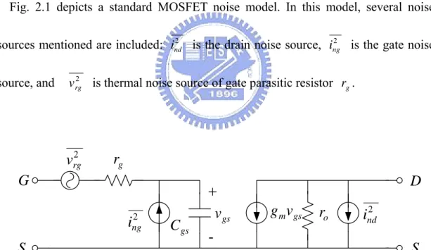
Fig. 2.1 depicts a standard MOSFET noise model. In this model, several noise sources mentioned are included: 2
nd
i is the drain noise source, ing2 is the gate noise
source, and 2 rg
v is thermal noise source of gate parasitic resistor r . g
G
S
gsC
D
S
2 ngi
v
gsg
mv
gsr
oi
nd2 2 rgv
r
g-+
2.1.2 Noise Factor of a Tow-Port Network
Noise factor F is a useful measure of the noise performance of a system. It is defined as the ratio of the available noise power Pno at its output divided by the product of the available noise power at its input Pni times the networks’s numeric gain G or equivalently defined as the ratio of the signal to noise power at the input to the signal to noise power at the output [5]. Thus
o o i i ni no N S N S G P P F / / = = (2-6)
The noise factor is a measure of the degradation in signal to noise ratio due to the noise from the system itself. Since the noise factor relates to the input noise power, a standardized definition of noise source has been setup: a resistor at 290K. A more general expression of noise factor NF is called noise figure which is just noise factor expressed in decibels:
F
NF =10log (2-7) When several networks are cascaded each having its own gain Gi and noise factor Fi, the total output noise is composed of all the noise from each stage but with different amount of contribution to the noise performance. The noise factor of a cascade networks is given as
... 1 1 2 3 1 2 1 + − + − + = G F G F F F (2-8)
low as possible and the gain of it should be as large as possible to suppress the noise of the following stage. The result is intuitive since the noise’s interference has less effect when the signal level is high.
2.1.3 Optimum Source Impedance for Noise Design
The noise factor of a two port network can be given as [5]
2 2 min | 1 | ) | | 1 ( | | 4 opt s opt s o n Z R F F Γ + Γ − Γ − Γ + = (2-9)
where Rn is the correlation resistance which tells us the relative sensitivity of the noise figure to departures from the optimum conditions and Zo is the characteristic impedance of the system. This equation expresses that there exists an optimum source reflection coefficient, Γ , or equivalently an optimum source impedance, opt Zopt, at
the input of the network in order to deliver lowest noise factor, Fmin. The value of Γ s
that provides a constant noise factor value forms non-overlapping circles on the Smith chart. It is usually the case that the optimum noise performance trades with the maximum power gain.
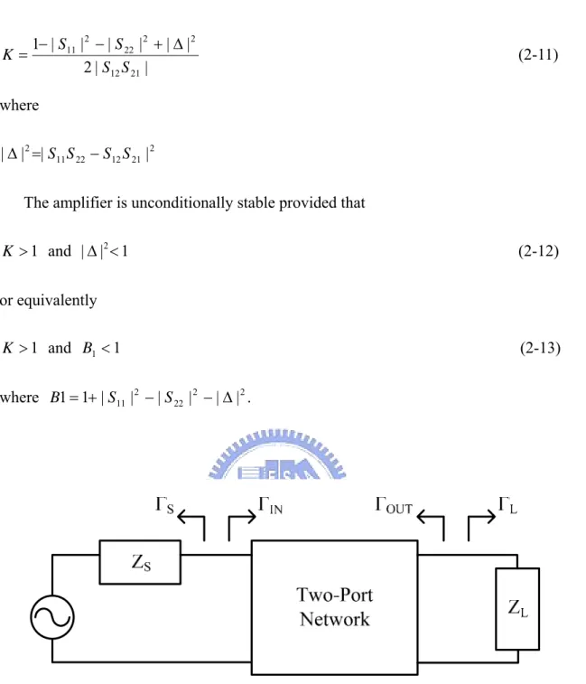
2.2 Amplifier Stability
The stability of an amplifier, or its resistance to oscillate, is a very important consideration in a design and can be determined from the S parameters, the matching networks, and the terminations [6]. The non-zero S12 parameter of a two port networks as shown in Fig. 2.2 provides a feedback path by which the power transferred to the output can be feedback to the input and combined together. Oscillation may occur when the magnitude of reflection coefficient Γ or IN ΓOUT, defined as the ratio of the reflected to the incident wave, exceeds unity. It is expected that a properly designed amplifier will not oscillate no matter what passive source and load impedances are connected to it [5], which is said to be unconditionally stable and the reflection coefficient is given as
1 | 1 | | | 1 | 1 | | | 11 21 12 22 22 21 12 11 < Γ − Γ + = Γ < Γ − Γ + = Γ s s OUT L L IN S S S S S S S S (2-10)
A network that has Γ >1 or IN ΓOUT>1 for certain load impedance is said to be conditionally stable. In such a case, input and load stability circles, the contour of
IN
Γ =1 and ΓOUT=1 for certain frequencies on the Smith chart, are useful to fine the boundary line for load and source impedances that cause stable and unstable condition. The stability circles can be calculated directly from the S parameters of the two port network, so another convenient parameter, stability factor K, is defined and given as
| | 2 | | | | | | 1 21 12 2 2 22 2 11 S S S S K = − − + ∆ (2-11) where 2 21 12 22 11 2 | | | |∆ = S S −S S
The amplifier is unconditionally stable provided that 1 > K and |∆|2<1 (2-12) or equivalently 1 > K and B1 <1 (2-13) where 2 2 22 2 11| | | | | | 1 1= + S − S − ∆ B .
Chapter 3
Low Power Double-Balanced Mixer
3.1 Introduction
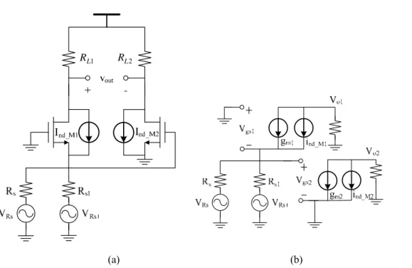
Mixer is an essential part of RF front-end circuits. Double balanced type mixer is more desirable than single-ended one for its better port-to-port isolation and even-order terms rejection. The received signal from the antenna is usually single ended. A phase splitter is needed to transform the signal from the proceeding stage, low noise amplifier (LNA), into a differential form to benefit from the double-balanced structure. To avoid unwanted signal loss, an active phase splitter is usually adopted [7][8]. However, the active phase splitter contributes limited gain and consumes lots of power. Therefore, in this work the phase splitter and transconductance stage are combined to a single stage to largely save power consumption. It consists of common gate and common source transistors which is claimed in [9] to have averagely good performance over other inspected types. The output balanced condition, the input matching, and the noise performance of the transconductance stage has been analyzed. PMOS switching stage with large size has bee selected for performance consideration.
The mixer under consideration is composed in an LC folded cascode structure [10] as shown in Fig. 3.1. Folded structure is a good configuration for low supply voltage and provides enough voltage headroom for transistors. The proposed structure of the mixer can not only meet the 1V supply requirement but also allow further reduction in the supply voltage level. Moreover, LC resonating removes unwanted harmonic signals so the linearity can be improved.
3.2 Transconductance Stage
3.2.1 Balanced Output Design
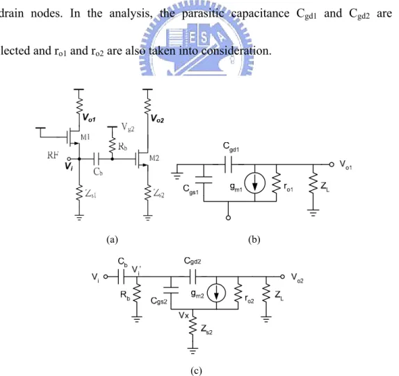
The transconductance stage consists of two transistors, a common gate transistor M1 and a common source transistor M2 as shown in Fig. 3.2(a). The RF input signal Vi is transformed into differential current by M1 and M2, respectively. The output differential current is then connected to the switching stage for current commutation, which loads the transconductor stage and makes the current into voltage Vo1 and Vo2 at drain nodes. In the analysis, the parasitic capacitance Cgd1 and Cgd2 are not neglected and ro1 and ro2 are also taken into consideration.
(a) (b)
(c)
Fig. 3.2 Common-gate common-source transconductance stage (a) schematic (b) small signal model of common gate and (c) common source parts.
Applying KCL to the small signal models shown in Fig. 3.2, the equations of output voltages to input voltage Vi is obtained as:
L gd o L L m o L i o Z sC r Z Z g r Z V V 1 1 1 1 1 / 1 / + + + = (3-1) ) / ( ) 1 ( 1 1 ) ( 2 2 2 2 2 2 2 2 2 2 2 2 2 2 2 2 2 2 2 2 2 2 2 2 2 L gs gs gd gd m o gd gs s m o L s gd L o gs gd gd m o gd gs s gd m i o Z C C sC C g r C C sZ g r Z Z sC Z r C sC C g r C C sZ sC g V V + + + + + + + + + + + + + + − = .(3-2)
Where ZL models the loading impedance of the switching pairs and Vi’ is assumed close to Vi at the operating frequency for the large capacitance Cb which is added to do the dc blocking. The large resistor Rb is used to give dc bias voltage and neglected in the analysis.
Suppose that Zs2 is equal to zero in (3-2), then (3-2) would be:
L gd o L L gd m i o Z sC r Z Z sC g V V 2 2 2 2 2 / 1 ) ( + + − − = (3-3) (3-1) and (3-3) must be equal in magnitude and out of phase at the operation frequency. Assume a pure resistance loading, ZL=RL, and equal size for the two transistors. The magnitude and phase of the two equations is extracted:
2 2 2 2 2 2 2 2 2 2 1 2 1 1 1 1 ) ( ) / 1 ( ) ( | | ) ( ) / 1 ( ) / 1 ( | | L gd o L L gd m i o L gd o L L m o i o R wC r R R wC g V V R wC r R R g r V V + + + = + + + = (3-4)
2 2 1 2 2 1 2 1 1 1 1 tan / 1 tan ) ( / 1 tan ) ( m gd o L L gd i o o L L gd i o g wC r R R wC V V Arg r R R wC V V Arg − − − ∠ − + ∠ − = + −∠ = π (3-5)
From (3-4) and (3-5), it is found that gm1 dose not exist in (3-5) that is gm1 could adjust the magnitude balance condition without any impact on the phase difference. Moreover, from (3-5), the phase difference of the two equations could be adjusted by one coefficient Cgd1 by adding a parallel capacitance Cex to the gate to drain capacitance of M1. Since Cgd1 will affect both the phase and gain difference, the Cex is defined to make the phase balanced first, then to adjust gm1 to meet the magnitude condition. The bias voltages of CG and CS stage are separated, so gm1 can be adjusted by gate voltage independently. The value of gm1 and gm2 would not be far apart, and the values of ro1 and ro2 are expected to be almost equal.
The input admittance Yin of the mixer can also be derived from the small signal model shown in Fig. 3.2:
CS in CG in in L o gd L o m gd gs CS in L o gd o m o o gs m s CG in Y Y Y Z r sC Z r g sC sC Y Z r sC r g r r sC g Z Y _ _ 2 2 2 2 2 2 _ 1 1 1 1 2 1 1 1 1 1 _ / 1 / 1 / 1 / 1 / 1 / 1 / / 1 1 1 + = + + + + + = + + + − + + + = (3-6)
Where Yin_CG is the input admittance of the common gate transistor M1 only and Yin_CS is the input admittance seen into the gate of the common source transistor M2. The real
part of the input impedance is mainly the parallel combination of 1/gm1 and Zs1. By Zs1, the gm value can be much more released, that is the power consumption can be much lower when making the input impedance matches to the source resistance.
3.2.2 Noise Analysis
Noise is analyzed in a simplified model which neglects both Cgs and Cgd, Zs1 is assumed to be Rs1 to evaluate the noise contribution of every part of the transconductance stage, especially Rs1 that is used to help input matching and power consumption. Only the drain current noise of the MOSFET and thermal noise of each resistor are taken into consideration. Based on Fig. 3.3, the noise power of each noise source contributes to the output is derived respectively. When calculate the noise
1
L
R RL2
(a) (b)
Consider for the thermal noise of Rs only: Vgs1=-Vgs2 (3-7) s RS gs s gs gs m o R V V R V V g i = = − +− 1 − 1 1 1 1 1 (3-8) 2 2 2 m gs o g V i = (3-9) From (2), ) / 1 / 1 ( 1 1 1 s s m s RS gs R R g R V V + + − = (3-10) From (1) to (4), the output noise current can be derived as:
2 2 1 2 1 1 2 2 1 2 _ ) ( ) / 1 1 ( 4 ) ( m m s m s s s no no R no g g R g R R kTR i i i s = − = + + + (3-11)
where i and o1 i are from the same noise source and are fully correlated to each o2
other.
The output noise current for Rs1 can be derived with the same procedure, and the equation is able to be written down immediately from (5). It is given as
2 2 1 2 1 1 1 1 2 _ ) ( ) / 1 1 ( 4 1 m m s m s s s R no g g R g R R kTR i s = + + + (3-12) The output noise from M1 is calculated by equations as follows:
Vgs1=-Vgs2 2 2 2 1 1 1 _ 1 1 1 || gs m o s s gs M nd gs m o V g i R R V i V g i = − = + = (3-13) From (7), ) || /( 1 1 1 1 _ 1 s s m M nd gs R R g i V + − = (3-14) From (7) and (8) 2 1 1 1 2 1 2 1 _ ) ) || ( 1 ) || ( 1 ( 4 s s m s s m m indM no R R g R R g g kT i + − = α γ (3-15)
As to M2, since the simplified model has no feedback path, Cgd1, the noise from M2 contributes directly to the output:
2 2 2 _indM 4 m no kT g i α γ = (3-16) The expression for noise figure is
2 _ 2 2 _ 2 _ 2 1 _ 2 _ 2 _ 1 1 s s s s R no indM no R no indM no R no R no i i i i i i F = + + + (3-17)
From (11), (12), (15), and (16), the noise contributed by M1 is much less than M2 when the parallel combination of Rs and Rs1 is approaching to 1/gm2. Take some values to give an approximate evaluation of each noise contribution. For Rs=50, gm1=gm2=0.015, γ/α=1, and Rs1=200, (3-17) would be
dB
F≈1+0.25+0.08+1.33=2.66=4.25 (3-18) The noises contribute by M2 is the main noise sources. The drain noise of M1 generates much less output noise as compared to M2 for its negative feedback function. However, if gm2 is increased to make the term be zero, the noise contributes by M2 is also increased. Moreover, the noise contributed by Rs1 is much large than that from M1.
3.3 LC-Folded Structure
The folded topology is a typical structure for low supply voltage consideration. The supply voltage of connected stages could be given respectively. An stacked structure
stage could be set differently. Though their biasing condition is independent, they are fully connected at high frequency for the frequency characteristic of LC tank. The LC tank is designed to resonate at the operation frequency. It is almost short at zero frequency so that DC supply voltage could be added through it. At the operating frequency, it provides very high impedance so that it will not degrade the differential current. Complete current could be transmitted to the switching stage for current commutation. At frequencies higher or lower to the center frequency, the impedance of LC tank is low. Therefore its resonate behavior forms a good filter to unwanted signals.
3.4 Mixing Stage
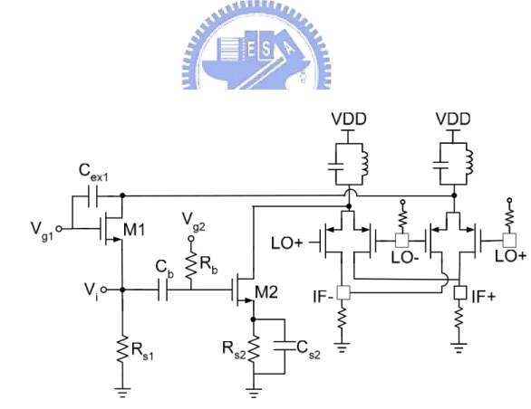
In this work, the proposed mixer utilizes current commutation for frequency mixing. A mixing stage is constructed to transform the incoming RF signal to a lower frequency. The non-ideal switching character and noise contribution will alleviate the circuit performance. To make the switching behavior more ideal, MOSFET of larger size is chosen and biasing point is set near threshold voltage. As pointed out in the beginning of this paper, the effort to convert signal into differential form is to make mixer in double-balanced structure. The issues of even-order distortion and LO-IF feedthrough are diminished in the double-balanced mixer.
Moreover, PMOSFET is chosen for its lower flicker noise. The flicker noise of MOSFET is appeared in low frequency range around DC, much lower than LO frequency, it can be effectively modeled as interference at the gate terminal of switching component. This slowly varying offset voltage disturbs the switching time, advancing or retarding the time of zero crossing. Mixed with the LO signal, the low frequency noise is up-converted to frequency around the LO frequency which degrades the function of mixing [11]. Therefore, the mixer topology is chosen as PMOS pairs. The complete circuit schematic is shown in Fig. 3.4.
3.5 Chip Implementation and
Measured Result
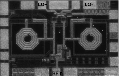
The die micrograph of the mixer fabricated in 0.18-um RF CMOS technology is shown in Fig. 3.5. The size of the chip is 1.04 x 0.67 mm2 including bonding pads. Measurements were conducted by chip-on-board setup as shown in Fig. 3.6. RF input and LO signals are applied through on-wafer probing with a GSG probe and GSGSG probes, respectively. A hybrid coupler is utilized to generate the LO differential signal from a single-ended signal. DC pads are wire-bonded on a PCB board, so as the differential IF signal. The output IF signal is buffered by an on-board unit gain operational amplifier circuit to convert to a single-ended form. Not to affect the IF loading condition, the differential input impedance of the OP amplifier is chosen as 16
LO+
LO-RFin
Kohm. A 50-ohm resistor is connected in series at the OP amplifier output for impedance matching to measurement system. Therefore, 6dB voltage gain shall be compensated in all the gain measurement.
The supply voltage Vdd is set as 1V in the measurements. The total DC power consumption is only 2 mW. The measured and the simulated input return loss centered at 5.5 GHz are shown in Fig. 3.7(a). The measured S11 is better than -10 dB within the wanted frequency band but for frequency higher than 4GHz, the measured S11 is worse than the simulated data. If is found on the Smith chart that the impedance is higher than 50Ohm. The input matching condition could be improved with higher bias voltage for larger gm. The RF signal is downconverted to 1 MHz. The measured conversion gain is 10.4 dB and the P1dB point is -6.8 dBm as depicted in Fig. 3.7(b). It is about 3.5 dB short as compared to the simulation. Two-tone test is done for measuring third-order intermodulation distortion. The maximum gain is corresponding to LO power equal to 2dBm as shown in Fig. 3.7(c). Fig. 3.7(d) shows that the measured IIP3 is about 3.8 dBm while the simulated IIP3 is about 0dBm. The noise figure is not tested for now and the simulated result is 9.9 dB.
RF port Probe G G S G G G S S LO port Probe Bond wire Vg1 Vg2 VDD Vgmixer DC Bias IF Output Buffer RF port Probe G G S G G G S S LO port Probe Bond wire Vg1 Vg2 VDD Vgmixer DC Bias IF Output Buffer
1 2 3 4 5 6 7 8 9 10 -24 -22 -20 -18 -16 -14 -12 -10 -8 S11 (dB ) Frequency (GHz) S11_Simulation S11_Measure -30 -25 -20 -15 -10 -5 0 0 2 4 6 8 10 12 C onver sion Gain (dB ) inpw (dBm) (a) (b) -12 -10 -8 -6 -4 -2 0 2 4 6 -2 0 2 4 6 8 10 12 Co nversio n Gain (dB) LOpw (dBm) (c) -40 -30 -20 -10 0 10 -75 -60 -45 -30 -15 0 15 Ou tpu t (dBm) RFin (dBm) IIP3=3.8dBm (d) Fig. 3.7 Mixer measured result (a) Input return loss (b) Conversion Gain (c) Conversion gain versus Lo
3.6 Summary
A 5-GHz double-balanced mixer is designed and fabricated in 0.18 CMOS technology. The circuit architecture is chosen available for the application of low supply voltage and low power consumption. The circuit consists a transconductance stage and PMOS switching pairs in a folded topology. Phase splitting function is integrated in the transconductance stage, which is composed of a common gate and common source transistors to save power consumption and to benefit from the double–balanced topology. Output balanced condition and noise of the transconductance stage are analyzed.
The measured input return loss and voltage conversion gain are 11dB and 10.4dB, respectively. The input third-order intercept point (IIP3) is 3.8dBm while consuming only 2mW from a 1V supply. Table I summaries the measured results of this work and compares the performance with other two circuits. Among these, [12] is a differential input mixer, and the power consumption must be increased since a phase splitting stage has to be added for single-ended input. As compared to the two circuits, this work has comparable gain and linearity while consuming the lowest power and lower supply voltage.
TABLE 3.1
Summary of measured performance and comparison to other mixers.
Item This Work Ref[10] Ref[12]
Technology CMOS 0.18um CMOS 0.18um CMOS 0.18um
RF Frequency (GHz) 5.5 2.4 2.4
DC Supply Voltage (V) 1.0 1.8 1
LO power (dBm) 2 - 0.5 Vp
Conversion Gain (dB) 10.4 16.5 11.9
IIP3 (dBm) 3.8 9 -3
Noise Figure (dB) 9.9 (simulate) 14.2 (DSB) 13.9 (SSB)
Chapter 4
Low-Power Front-End Circuit
4.1 Introduction
To meet the low supply voltage requirement, the conventional cascode topology is dismissed, a single transistor structure is adopted instead for the LNA. The issue of this structure is the stability problem, and it has been tackled in our design. A figure of merit is also presented to find an optimum biasing point for transistors under low supply voltage as low as 0.6V.
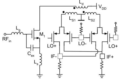
Transformer ac coupling is an effective way to realize a low power front-end circuit. It can not only cut down the supply voltage [13], but also do the phase transformation
IF- IF+ LO+ LO-LO+ VDD M1 Ld LS1 RFin Lg Ls Cex LS2
without extra power consumption [14]. The transformer design relates to many design variables, to analyze and design with a quick convergence to the optimum condition is realistic for fabrication. In this work, based on resonant operation idea [15], a transformer is designed to transform single-ended signal from the LNA into differential current with current conversion gain to realize a low power receiver front-end circuit.
Fig. 4.1 shows the circuit schematic of this receiver front-end. The design consideration of each stage is discussed in the following sections.
4.2 Low Noise Amplifier
4.2.1 MOSFET I-V Model
A semi-empirical, single-piece expression that provides good accuracy in moderate inversion and acceptable accuracy in weak and strong inversion is given by [16]
} )] 1 [ln( )] 1 {[ln( 2 2 2 t 2 ds th gs t th gs n nV V V n V V do ds I e e I φ φ − − − + − + = (4-1) where L w n C Ido =µ ox2 φt2 q kT t = /
φ is the thermal voltage. The parameter n whose value depends on the
process describes the rate of exponential incrase of Ids with Vgs in the subthreshold region. Its value varies from 1.1 to 1.9 which is higher for short channel devices. When MOSFET operates in weak inversion region, the exponential terms in (4-1) are small and with log(1+x)≈x for x<<1, (4-1) reduces to
t th gs t ds n V V V do ds I e e I φ φ − − − ≈ (1 ) (4-2) For the strong inversion region, log(1 )2 log( )2 2
y e ey ≈ y = + , (4-1) is reduced to ] 2 1 ) [( 2 ds ds th gs ox ds V V V nV L w C I =µ − − (4-3) for linear region, and it is simplified to
n V V L w C Ids ox gs th 2 ) ( − 2 =µ (4-4) for strong inversion where MOSFET in the linear RF blocks are usually biased. In the
saturation region, the second exponential in (4-1) becomes negligible, and (4-1) reduces to 2 2 )] 1 {[ln( t th gs n V V do ds I e I φ − + = (4-5) From the semiconductor concept, the MOSFET’s operation region makes a transition from weak to moderate inversion region if both the minority and the majority carrier concentrations become equal. To determine the bias transition from the I-V relation of MOSFET, the exponential part of (4-5) is approximated
as( )2
th gs V
V − when Vgs −Vth >>2nφt. Thus, the upper limit of moderate inversion
region is roughly defined as the gate-source voltage at which 2 =10
− t th gs n V V e φ or
Vgs-Vth=4.6nφt [17]. The boundary value for the transition for n as 1.1 to 1.9 ranges
from Vgs-Vth=0.131 to Vgs-Vth=0.226.
4.2.2 Optimum Design- New Figure of Merit
LNA typically consumes much more power than that of the other parts to provide enough gain to the receiver front-end circuit. In order to maintain low power consumption, the biasing current of the LNA is desired to be as low as possible. Therefore, there exists a compromise between the current consumption, ID, and the transconductance, gm, of the MOSFET to keep the gain of the circuit. A conventional
the frequency response of a device into consideration. Another figure of merit, gmft/ID, [17] which adds unit gain frequency into it to evaluate the frequency response of the MOSFET is therefore defined and an optimum design point is found by using this parameter, which is moderate inversion region of a MOS transistor.
But this figure of merit is not effective as the supply voltage level goes down. As shown in fig. 4.2, where the x axis is the biasing current, ID, and the y axis is the production of gm and ft divided by ID, both of which are not normalize but it has no effect on the conclusion. Fig. 4.2(a) takes supply voltage, VDD, as 1 V and 0.8 V, respectively. Sweep the bias voltage, Vgs, from zero to VDD, a maximum value of the figure of merit is reached when Vgs is about 0.6V. But when the supply voltage is lowered further to 0.6V, as shown in fig. 4.2(b), no optimum point would exist. The value of the figure of merit keeps flat when Vgs approaches VDD, 0.6V.
To decide an optimum design point around 0.6V, linearity of the MOS transistor is
0 1 2 3 4 5 -0.05 0.00 0.05 0.10 0.15 0.20 0.25 0.30 0.35 0.40 g m f t /I D ID (mA) VDD=0.8V VDD=1V Vgs=0.6V 0.0 0.1 0.2 0.3 0.4 0.5 -0.05 0.00 0.05 0.10 0.15 0.20 0.25 0.30 0.35 0.40 gm ft /ID ID (mA) VDD=0.6V (a) (b)
added to define a figure of merit for MOSFET: ) 1 ( 3 min − F I IIP f g D t m (4-6)
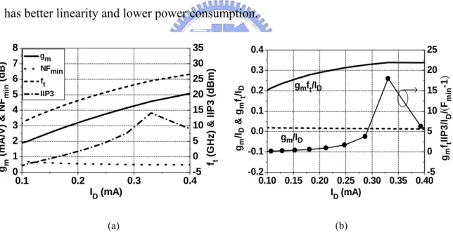
which has been used as a figure of merit for LNA. As shown in fig. 4.3(a), IIP3 has an optimum value around that flat region. Fig. 4.3(b) shows the new figure of merit. Therefore, the bias condition of LNA is chose as 0.58V.
However, the load impedance affects the position of the IIP3 peak and should be taken into consideration as discussed in section 4.4. Therefore, a modified version of this circuit was re-taped out. The second chip of the front-end trades little gain while has better linearity and lower power consumption.
-5 0 5 10 15 20 25 30 35 0.1 0.2 0.3 0.4 0 1 2 3 4 5 6 7 8 gm (mA/V ) & NF min (dB) ID (mA) gm NFmin ft IIP3 f t (GHz) & IIP 3 (dBm) -5 0 5 10 15 20 25 0.10 0.15 0.20 0.25 0.30 0.35 0.40 -0.2 -0.1 0.0 0.1 0.2 0.3 0.4 gm /ID & g m ft /ID ID (mA) gmft/ID gm ft IIP 3 /ID / ( Fmi n -1 ) gm/ID (a) (b)
Fig. 4.3 Character of a transistor (a) Parameters variation of a transistor (b) Several figure of merits for a transistor.
4.2.3 LNA Stabilization
Cascode configuration shown in Fig. 4.4(a) is conventionally adopted for LNA design. It has good isolation between the input and output port. However, as the supply voltage goes down, cascode configuration is not applicable. A single transistor configuration as shown in Fig. 4.4(b) is preferred. The Cgd feedback path causes the circuit isolation become poor. The load inductance connected to the drain of the transistor falls into the unstable region for a common source transistor. Therefore, an effort is needed to make sure the circuit is stable.
Fig. 4.5 is the source and load stability circle of a single transistor from 0.1GHz to 10GHz. As shown in this figure, the load stability circle of a common source transistor typically cuts the upper region of the smith chart. There is no stability issue for the cascode topology since the load of the common source transistor is usually
Vdd
Cgd
(a) (b)
capacitive and locates at the stable region. However, the load in our design is potentially inductive. To improve the stability of the two port network, a small signal model shown in Fig. 4.6(b) is used to calculate the input resistance when an inductor being its load and two passive components added as in Fig. 4.6(a). The input impedance is derived as )] ( ) ( ) [( ) 1 )( 1 ( 2 2 2 d s gd gs d s gd m gd gs d gd s gs s m L L C C s L L C sg C C s L C s L C s L sg Zin + + + + + + + + = (4-7) Assuem d s gd m s m d s gd gs s gs d gd d s gd gs gd gs d s gd m L L C g w L wg d L L C C w L C w L C w c L L C C w C C w b L L C g w a b a cb ad j b a bd ac jb a jd c Zin 3 4 2 2 2 2 2 2 2 2 1 )] ( ) [( ) ( − = + − − = + − + = + − = + − + + + = + + = (4-8)
To make sure the real part of the input resistance is positive, ac+bd must be positive.
indep(L_StabCircle1) (0.000 to 51.000) L_St abC irc le1 indep(S_StabCircle1) (0.000 to 51.000) S_S tabC irc le 1
After some calculation, the equation is given as 0 ) 1 )( ( − − 2 > w L C L C L Cgs s gd d gd d (4-9)
The input resistance might be negative due to the inductive load. The second term in (4-9) would not be negative up to several tens of gigahertz. Therefore, the multiplication of Cgs and Ls must be larger than CgdLd to improve the circuit stability. The result is quite intuitive since the gain of the circuit degrades due to these added components. The above analysis gives a hint to improve stability, though it is not complete. The output port should also be checked. However, as shown in Fig. 4.5, the source stability circle cuts less to the Smith chart and the source impedance is typically 50 Ohms which is far out of the stability circle.
Cex Ls Vdd Ld Cd (a) (b)
Fig. 4.6 Schematic and small signal model of proposed LNA (a) The transistor with stabilization elements. (b) small signal model of (a).
Fig. 4.7(a) depicts the simulation result of load stability circle’s variation when these two passive components are added to a single transistor. Fig. 4.7(b) shows the variation of K for Cex and Ls. The K does grow high as LsCex gets higher. The K is still less than 1, so the circuit is still conditionally stable. But as Fig. 4.7(a) shows, the stability circle does moves more out before stabilization.
Since the higher the Cex and Ls is, the lower the gain and the higher the NFmin would be, these values are chosen to be properly large to make sure the load impedance locates outside the stability circle for all the frequencies. As shown in Fig. 4.8, the Ls is 0.9nH and Cex is 100fF.
MOS only Ls added
Ls and Cex added
Stability Circle (5.5GHz) 0.17 0.25 0.34 0.42 0.51 0.59 0.68 0.76 0.85 50 100 150 200 250 300 0.2 0.4 0.6 0.8 1.0 1.2 1.4 1.6 L s (nH) C ex (fF) [email protected] (Q of L s = 10) (a) (b)
Fig. 4.7 Stability variation with stabilization (a) Stability circles before and after stabilization (b) K of a transistor with Ls and Cex
4.3 Mixer Consideration
The transconductor of the mixer is the transformer stage. The transformer converts input signal into differential current output and then sends into the mixing stage. The design consideration for the first chip of the front-end circuit is based on the idea discussed in Section 3.4. However, the mixing stage has to be activated by large LO power which dose not conform to the idea of low power consumption. Therefore, the modified version re-considers the design procedure. Gate bias voltage, LO power, and load resistance RL are the design variables. The conversion gain begins to decrease when the MOSFET operation suffered from compression, which is about 0.2 to 0.3V for drain to source voltage VDS.
indep(L_StabCircle1) (0.000 to 51.000) L_ St ab C irc le1 freq (1.000GHz to 10.00GHz) _20 070 525 _new _lo adin g. .S (1, 1 ) Frequncy from 1GHz to 10GHz Load stability circle
Load impedance indep(L_StabCircle1) (0.000 to 51.000) L_ St ab C irc le1 freq (1.000GHz to 10.00GHz) _20 070 525 _new _lo adin g. .S (1, 1 ) Frequncy from 1GHz to 10GHz Load stability circle
Load impedance
Therefore, for larger RL, the LO power for highest gain is smaller while the power consumption is smaller. And for lower gate bias voltage, or said larger VSG for PMOS, the LO power for highest gain is also smaller. Fig. 4.9 depicts the current to voltage conversion gain of the mixing stage with different RL for a given gate bias voltage 0.16V. Since the gain gets saturated when RL large, the selected RL is 1600 Ohm and the LO power is -7.5dBm.
-10 -8 -6 -4 -2 0 34 36 38 40 42 44 46 48 50 A I R L (dB) LO power (dBm) RL=1200 RL=1600 RL=2000 RL=800 RL=400
4.4 Transformer Design
Transformer is used as the phase splitter stage for this circuit. Differential current has been generated from a single-ended input for the following stage with no extra power consumption. However, the conversion loss of a conventional transformer design trades the benefit of power, since a higher power consumption of LNA is required to overcome the loss. Based on the idea of resonant operation mentioned in [15], two coupled resonant networks, each of which composed of a capacitor and an inductor, have resonant frequency w1 and w2, respectively, can result in a high current gain of the transformer. In this way, there is no need to increase the power of the LNA stage and the phase splitting can be done with current conversion gain under no extra power consumption so that low power consumption is achieved. Moreover, the AC coupled DC blocked character makes LNA and Mixer connected in a folded topology. Low supply voltage is therefore realized.
4.3.1 Equivalent Model for the Transformer
There are some main parameters regarding to describe a transformer. One of them is turn ration n: 1 2 L n L = (4-10) where L1 and L2 are the self-inductances of the primary and secondary windings,
respectively.
The self-inductance, which is relates the voltage induced in a winding by a time-varying current in the same winding, is extracted at the terminals with other windings open-circuited. For monolithic transformers, the turn ratio value is not equal to the turn ratio of the layout, since the physical length of the inside and outside turns are not equal. Besides, the arrangement of the alternative windings affects the self-inductance of each winding.
Another is the magnetic coupling coefficient k:
1 2
M k
L L
= (4-11) where M is the mutual inductance, which is the ability of one inductor or segment to induce a voltage across the neighboring inductor or segment when they are close enough.
There are mutual inductance between two inductors and different segments of a single inductor. The mutual inductance linking these two could be positive or negative to the total inductance of each of them. For two segments with current flow in the same direction, the mutual inductances are positive. But for two segments with current flow in opposite direction, the mutual inductances are negative. k is a measure of the magnetic coupling between two windings and ranges from zero, uncoupled condition, to unity, perfect coupling. For passive elements, the magnitude of the
coupling coefficient may not exceed unity.
Fig. 4.10(a) is a figure of transformer with loads Z1 and Z2 and Fig. 4.10(b) is a simple equivalent model for the transformer. L1 and L2 are the self-inductances of the windings. M is the mutual inductance between the two windings. Rs1 and Rs2 are the ohmic losses of the windings. Z1 and Z2 are not only the source and load impedances but also have to include parasitic capacitances of the transformer, as the model adopted later. The input impedance Zin1 can be derived as
2 2 1 1 1 2 2 2 = + + + + in s s w M Z R SL Z R SL (4-12) For an ideal transformer, which is defined to has unity coupling coefficient, and infinite self-inductances with no loss, the input impedance is
M L1 L2 Rs1 Rs2 Z2 Z1 (a)
M
R
S1L
1-M
L
2-M
R
S2 Zin1 Zin2Z
1Z
2 (b)2 in1 2
Z =Z n (4-13) which is quite different from the input impedance derived for non-ideal case. Though both of them depict the ability of impedance transformation, the n2 ratio may not be realistic in reality and depends on the inductances and mutual inductances.
4.3.2 Derivation and Design of Resonant Operation
for Current Gain
Before calculating for the current transfer equation, let’s take a look at resonant network[15] which is composed of two LC resonant circuits with some mutual coupling between them as shown in Fig. 4.11. The resonant frequencies are w1 and w2, respectively. 2 2 2 1 1 1 1 , 1 C L C L = = ω ω (4-14)
Let w =mw . The two resonant frequencies of this system can be derived as Fig. 4.11 Resonant system
2 4 2 2 2 2 2 1 2 4 1 2(1 ) + ± − + + = − r m m m k m w w k (4-15) where ) 1 ( 2 1 4 2 1 ) 1 ( 2 1 4 2 1 2 2 2 2 4 2 2 2 2 2 2 4 2 2 k m k m m m w w k m k m m m w w L H − + + − − + = − + + − + + = (4-16)
For two resonators of the same frequency wo, m=1, when there exists some coupling between them, the coupled system’s resonant frequency will depart from wo due to the coupling coefficient. For two resonators of different resonant frequency, the systems resonant frequency will depend not only on k, but also on their separate resonant frequencies. When the resonant system resonant at the desired frequency, no matter it is of the higher resonant frequency or the lower one, the current gain can be relatively high.
Let’s consider for the model to calculate for the current transfer equation of the fabricated transformer. Since the signal is differential at the second turn, there exists a virtually short point for the transformer, the center tape, and two of the switching pairs of the front-end circuit are turned on by the LO signal. The simplified equivalent
circuit for the half path of Fig. 4.1 can be shown as Fig. 4.12. Rs and RL are the source and load impedances which are extracted from the former stage, LNA, and the following stage, switching stage, respectively. C1 and C2 are the parallel combination of the parasitic capacitances of transformer and that of the stages connected to it. With the definition of following coefficients, the transfer function would be a function of five variables, m, k, n, L1, and C1 when Rs, RL, w, and α are defined.
2 2 1 1 2 1 2 1 2 1 1 1 2 2 L R L R L L M k L L n w w C L C L m α α = = = = = = (4-17)
The current transfer function is (4-18) which is given as:
)]} 1 )( ( )][ ( [ )]} ( )[ 1 ( { ){ 1 ( )] 1 )( ( [ ) ( 1 1 1 2 2 1 1 1 2 1 1 1 sL sRC sRC sM R sRC R sL M R sL M Rs R sL sRC R R R M sR I I s G s s s L s s L s in out + + + − + + − + + + + + + + + = =
To design the transformer for resonant operation, (4-16) are assumed equal to operation frequency in turn and w is therefore solved for given m and k condition.
M
Iin RS C1 C2
RS1 L1-M L2-M RS2 Iout
RL
Once w2 is found, w1 is also known. The remained unknowns are the L1 and L2 values, which is equivalent to L1 and n, and C1 and C2, the last two unknowns, can be derived after these two values are defined. There are lots of possible solutions for L1 and n. All these solutions satisfy the resonant operation condition. But among them, the rules of L1 and n combination which gives the highest possible gain need to be found out. Since the target of the design is to find high gain solution, (4-18) is calculated for sets of L1 and n. Fig. 4.13 to Fig. 4.15 are the gain variation condition with solutions of L1 and n under certain m and k combination. The current gain is calculated for: Rs=7.675kΩ, RL=276Ω, α=1Ω/nH case. Rs and RL is the extracted ro of LNA and operation parallel 1/gm of the switching pair.
1.07 1.27 1.48 0.866 1.68 0.662 1.89 0.458 1 2 3 4 5 6 7 8 9 10 0 1 2 3 4 5 6 7 8 9 10 Turn Ratio n L 1 (nH) m=0.6, k=0.45, α=1 fH=11.28, f1=5.77, f2=9.61 0.494 1.12 1.32 1.53 1.74 1.84 0.908 1.94 0.701 2.05 1 2 3 4 5 6 7 8 9 10 0 1 2 3 4 5 6 7 8 9 10 Turn R a tio n L1 (nH) m=0.6, k=0.65, α=1 fH=14.29, f1=5.99, f2=10.0 (a) (b) 0.5280.946 1.16 1.36 1.57 1.78 1.99 0.737 0.528 1 2 3 4 5 6 7 8 9 10 0 1 2 3 4 5 6 7 8 9 10 Tu rn R a tio n L1 (nH) m=0.6, k=0.85, α=1 fH=22.31, f1=6.23, f2=10.38 (c)
Fig. 4.13 Current gain relative to n and L1. Set fL=5.5GHz, m=0.6 (a) k=0.45 (b) k=0.65 (c) k=0.85
1.08 1.27 1.47 1.67 1.87 0.876 0.677 0.478 1 2 3 4 5 6 7 8 9 10 0 1 2 3 4 5 6 7 8 9 10 Tu rn R a ti o n L 1 (nH) m=1, k=0.45, α=1 fH=8.93, f1=f2=6.62
Assumed three conditions: m=0.6 (m<1), m=1, m=1.4 (m>1) and set lower resonant frequency fL as 5.5GHz. The condition for higher gain is limited to certain turn ratio and the calculated gain becomes saturated for that turn ratio as L1 gets larger. For larger m (w1 is higher than w2), the turn ratio for higher gain is moved to larger region than smaller m case. The current gain gets higher as k larger. No matter what the m value is, the current gain has close order of magnitude. But for m<1 and
0.239 0.761 0.935 1.11 1.28 1.46 1.63 0.587 0.413 1 2 3 4 5 6 7 8 9 10 0 1 2 3 4 5 6 7 8 9 10 Turn Ratio n L 1 (nH) m=1.4, k=0.45, α=1 fH=10.0, f1=f2=5.92
fL=5.5GHz case, the current gain can be larger than the turn ratio due to the resonant operation mode. Moreover, for m>1 and lower resonant frequency fH=5.5GHz case, the current gain can also be larger than the turn ratio as shown in Fig. 4.16.
For k higher, the current gain is getting lower for fH equal to 5.5GHz case. Although the current gain larger than turn ratio for m>1 case, the magnitude under this case is much lower than setting fL to 5.5GHz cases. Therefore, it is better to design fL as the
0.137 0.180 0.224 0.268 0.311 0.355 0.0932 0.398 0.0496 1 2 3 4 5 6 7 8 9 10 0 1 2 3 4 5 6 7 8 9 10 Tu rn R a tio n L1 (nH) m=0.6, k=0.45, α=1 fL=2.68, f1=2.81, f2=4.69 0.464 0.578 0.691 0.350 0.805 0.237 0.918 0.124 1.03 1 2 3 4 5 6 7 8 9 10 0 1 2 3 4 5 6 7 8 9 10 Tu rn Rati o n L1 (nH) m=1, k=0.45, α=1 fL=3.39, f1=f2=4.08 (a) (b) 0.445 0.298 0.591 0.738 0.884 0.152 1.03 1.18 1.32 1 2 3 4 5 6 7 8 9 10 0 1 2 3 4 5 6 7 8 9 10 Turn Ratio n L1 (nH) m=1.4, k=0.45, α=1 fL=3.03, f1=4.56, f2=3.26 (c)
Fig. 4.16 Current gain relative to n and L1. Set fH=5.5GHz (a) m=1.4, k=0.45 (b) m=0.6, k=0.45
As mentioned in last few paragraphs, for fL=5.5GHz case, the current gain for different m is quite close and the gain is higher for larger k, how to make decision for these parameters? The constraint is given by the unavoidable parasitic capacitance of the transformer and that of the stages connected to transformer. C1 is typically the limit since the turn ratio larger than one means smaller L2, then calculated C2 is usually quite large. Fig. 4.17 shows the calculated C1 value for Fig. 4.13 (a) and (b). When the coupling coefficient gets larger, the calculated resonant frequency w2
500 200 160 120 80.0 1 2 3 4 5 6 7 8 9 10 0 1 2 3 4 5 6 7 8 9 10 Tu rn R a tio n L 1 (nH) m=0.6, k=0.45, α=1 fH=11.28, f1=5.77, f2=9.61 500 200 160 120 80.0 1 2 3 4 5 6 7 8 9 10 0 1 2 3 4 5 6 7 8 9 10 Tu rn Ratio n L 1 (nH) m=0.6, k=0.65, α=1 fH=14.29, f1=5.99, f2=10.0 (a) (b) 200 160 120 80.0 1 2 3 4 5 6 7 8 9 10 0 1 2 3 4 5 6 7 8 9 10 Turn Ra tio n L1 (nH) m=1, k=0.45, α=1 f H=8.93, f1=f2=6.62 (c)
becomes larger which means a larger w1. Then the C1 would become smaller as shown in Fig. 4.17(a) and (b). When m is larger, even though w2 is smaller, w1=mw2 is not necessary smaller since m increases. The m large case’s gain is limited by the C1 and achievable gain might be low.
By the inductor model of TSMC, one can estimate the parasitic capacitance of the transformer and then decide the parameters. Fig. 4.18 shows the frequency response of several inductors, by the resonant frequency of the inductor, the parasitic capacitance is estimated as 52fF for 4.7nH inductor. The parasitic of the transformer is expected to be larger than that of the inductor. Besides, the capacitance looked back into the LNA also needs to be considered. Then, the C1 limit is set as 150fF for a 4.5nH inductor. Since the C limit of higher k is smaller, and the gain level of higher k
0 2 4 6 8 10 12 14 16 18 20 -800 -600 -400 -200 0 200 400 600 800 Im a g( z) Frequency (GHz) 3.2nH 7.9nH 6.2nH 4.7nH TSMC 018 Inductor_STD
Space=2um, Width=9um, Turn=4.5