國 立 交 通 大 學
光電工程研究所
碩 士 論 文
低溫鈍化絕緣層技術應用於鍺型金氧半元件
之研究
Study of Low Temperature Post-gate Dielectric
Treatment for Germanium-based MOS Device
研 究 生 : 林 敬 儒
指導教授 : 劉 柏 村 博士
中 華 民 國 九十九 年 八 月
低溫鈍化絕緣層技術應用於鍺型金氧半元件之研究
Study of Low Temperature Post-gate Dielectric Treatment for
Germanium-based MOS Device
研 究 生:林 敬 儒 Student:Jing-Ru Lin
指導教授:劉 柏 村 博士 Advisor:Dr. Po-Tsun Liu
國 立 交 通 大 學
光 電 工 程 研 究 所
碩 士 論 文
A Thesis
Submitted to Department of Photonics Institute of Electro-Optical Engineering College of Electrical and computer Engineering
National Chiao Tung University In partial Fulfillment of the Requirements
the Degree of Master In Electro-Optical Engineering June 2010
中 華 民 國 九十九 年 八 月
低溫鈍化絕緣層技術應用於鍺型金氧半元
件之研究
研究生:林 敬 儒 指導教授:劉 柏 村 博士
國 立 交 通 大 學
光電工程研究所
摘要
鍺半導體由於擁有較高的電洞和電子遷移率,被視為是下一世代奈米電子元 件技術中最有希望取代矽而成為電晶體主動層的半導體材料,但是氧化鍺的熱穩 定性較差,使得元件製作過程中的高溫製程將會劣化Ge-MOSFET 的元件特性。 因此,在我的論文裡,我們提出了一種低溫的超臨界流體技術,針對氧化鍺的熱 穩定問題去進行探討。目的是為了利用低溫的處理技術,去改善因為氧化鍺熱解 的問題對元件造成裂化的影響。我們研究了鍺型金氧半元件在超臨界二氧化碳流 體混合水的熱處理下其電性的改變。首先,我們使用了溫度約150°C 超臨界流體 混合水的技術,直接對剛沉積完的二氧化矽做處理,我們後續使用了高解析穿透 式電子顯微鏡以及 X 光光電子能譜儀,驗證超臨界流體混合水能有效的使水分 子通過二氧化矽到達鍺通道和二氧化矽的界面,進而氧化鍺表面產生鍺型氧化物, 使得閘極氧化層厚度增加,並且減少界面的缺陷密度。從電容-電壓曲線可以驗 證在經過超臨界處理過後,在中高頻的頻率之下,反轉區的電容值可以有效的被 抑制,顯示出超臨界流體具有鈍化鍺通道表面缺陷的能力。在者,我們發現在經 過450°C 30 分鐘的真空退火之後,發現元件有裂化的情形產生,使得閘極電容下降,漏電流上升,推測跟二氧化鍺的熱解有關,然而在對經過退火後的元件作 超臨界處理,我們發現元件特性得到改善,不論是閘極電容值抬升,漏電流下降, 都顯示出超臨界二氧化碳流體混合水的確具有通過閘極氧化層進而深入到鍺通 道表面去鈍化缺陷的能力。 除此之外,我們利用電子槍真空蒸鍍系統,在低溫下製造二氧化鋯/二氧化 鍺元件結構,但不可避免地,在低溫沉積過程中,由於懸鍵和氧空缺的產生,使 得元件的特性不佳,而適當的退火可以讓二氧化鋯的薄膜品質變好,並降低界面 缺陷。但在600°C 30 秒的快速退火後,卻遇到二氧化鍺熱解的問題,使得元件 漏電大量抬升,藉由漏電機制的探討可以知道,漏電抬升的原因是因為二氧化鍺 熱解問題所產生的淺層缺陷所致,然而在經過後續的超臨界處理,我們發現這些 淺層缺陷可以有效的被修補,使得漏電可以被抑制,並且擁有較好的元件特性。 由這些結果顯示,顯示藉由低溫超臨界流體混合水的技術,能減少薄膜的缺 陷密度,並且改善鍺型元件在界面的特性。可預期的,若將超臨界流體的特殊特 性整合在鍺型電晶體元件的製作上,去修補因為後續高溫製程對元件產生的裂化 情形,對於未來高效能鍺型MOSEFT 發展,將具有其優勢以及前瞻性。
Study of Low Temperature Post-gate Dielectric
Treatment for Germanium-based MOS Device
Student:Jing-Ru Lin Advisor:Dr. Po-Tsun Liu
Department of Photonics Institute of Electro-Optical Engineering
National Chiao Tung University
Abstract
In this study, supercritical fluids (SCF) technology is employed originally to effectively improve the properties of low-temperature-deposited metal oxide dielectric films. In this work, 2μm Ge film are epitaxy on p-type Si by CVD, and 13nm SiO2 was deposited by LPCVD as gate oxide insulator. Then we divided two parts for study in this work. The first part, the supercritical fluids was applied on the as-deposited SiO2 film. By HR-TEM, XPS analyses to verify the capacity of delivering H2O molecule into the SiO2 films for repairing defect states. A smooth interfacial GeO2 layer between gate SiO2 and Ge is thereby formed after SCF treatment, and the frequency dispersion of capacitance-voltage characteristics is also effectively alleviated. The second part, the electrical degradation of Ge-MOS after a post-gate dielectric annealing at 450°C, as the SCF treated, it can be restored to an extent similar to the initial state.
Additionally, supercritical fluids technology is also proposed to effectively remove the shallow traps in ZrO2/GeO2 stacks after 600°C annealing, which defects are created by GeO2 decomposition makes GeO desorption to enhance the device
leakage increasing obviously. As SCF treated, the leakage was suppressed and the shallow traps are reduced by current mechanism fitting. The low temperature SCF treatment on high performance Ge-MOSFET shows promise as critical technology in resolving GeO2 decomposition.
誌 謝
兩年的碩士生活,一眨眼就過去了,兩年的林林總總讓我可以順
利的完成我的碩士論文。首先我要先感謝我的指導教授:劉柏村教授,
提供完好的研究環境以及豐富的資源,並且在實驗上給予我寶貴的意
見讓我受益良多。
再來要感謝的就是帶我的震鑠學長,雖然學長對實驗的要求比較
嚴苛,但學長總是不厭其煩地教導我實驗的方法與想法,且樂於與我
互相討論實驗上的問題,讓我這兩年來成長許多。接著要感謝的是帶
我學機台的小猪學長、虛胖學長和阿寶學長,感謝你們帶我入門實驗
機台,讓我可以順利低上手完成自己的實驗。還有虛胖學長,在實驗
上也幫了我需多的忙,不論是在國科會貴儀上的預約,材料分析送件
及分析,給予我許多的協助。
再來要感謝的是一德學長、立峰學長和立煒學長,雖然在研究上
比較沒交集,然而在我需要幫忙的時候,也依然不吝嗇的提供一些寶
貴的意見給我做參考。
再來感謝光廷、俊傑、治翔、富海,有你們這麼好的同學,讓我
在這兩年過得很開心,大家偶爾白爛一下,一起吃飯一起出去玩,一
起努力,即使在實驗上總是遇到許多的不順和困難,大家也是一起咬
著牙,也順利的撐過去了。恭喜大家都順利一起畢業。
再來感謝明聰、楊順和孟娟,特別感謝明聰學弟在實驗上的協助
和幫忙。
最後感謝我的父親林進南先生,母親張麗美女士,多年來對我的
栽培和鼓勵,讓我可以在求學的路途上無後顧之憂,在自己的路上衝
刺。也謝謝老妹和朋友們一直給予我支持和幫忙,讓我可以克服許多
問題和面臨到的困難,有你們的協助,讓我得以在兩年的碩士生活順
利完成我的學業。
林敬儒 2010 年 8 月
Contents
Chinese Abstract --- i
English Abstract --- iii
Chinese Acknowledgment --- v
Contents --- vi
Table Captions --- ix
Figure Captions --- x
Chapter 1 Introduction
1.1 General background --- 1 1.2 Motivation --- 3 1.3 Organization of thesis --- 5Chapter 2 Effects of Supercritical Fluid (SCF) and Post-Deposition
Annealing (PDA) on the SiO
2/Ge MOS Capacitor
2.1 Fabrication of Metal Oxide Semiconductor Capacitor and Experiment Process --- 72.2.1 High-Resolution Transmission Electron Microscopy Analysis ---- 8
2.2.2 CV Characteristics with Various SCF Treatments --- 9
2.2.3 X-ray Photoelectron Spectroscopy (XPS) Analysis --- 10
2.3 The Thermal Stability and the Effects of SCF Treatment on PDA-Treated SiO2/epi-Ge MOS --- 10
2.3.1 Effects of the Thermal Stability on SiO2/epi-Ge Capacitor --- 10
2.3.2 Effects of SCF Treatment on PDA-Treated Ge-MOS --- 11
2.4 Summary --- 12
Chapter 3 Effects and mechanisms of PDA and following SCF
treated on the ZrO
2/GeO
2/Si MOS capacitor
3.1 Fabrication of ZrO2/GeO2 Stack with MOS Capacitor and Experiment Process --- 193.2 Effects of PDA on the ZrO2/GeO2/Si MOS Capacitor --- 20
3.2.1 Parameter Description --- 20
3.2.2 Characteristics of CV and IV Curves --- 21
3.3 Leakage Mechanism Transferred After Post-SCF Treated --- 23
3.3.1 Characteristics of JV Curves --- 23
3.3.2 Conduction Mechanisms --- 24
3.4 Various SCF-liked Treatments on ZrO2 Thin Films --- 27
Chapter 4 Conclusions and Suggestions for Future Work
4.1 Conclusions --- 44 4.2 Suggestions for Future work --- 45
Table Captions
Chapter 1
Table 1-1 Critical temperature and pressure for some common fluids.
--- 6
Chapter 3
Table 3-1 Pure ZrO
2parameters extraction by P-F emission fitting.
--- 38
Table 3-2 Pure ZrO
2parameters extraction by TAT fitting. --- 38
Table 3-3 ZrO
2/GeO
2parameters extraction by P-F emission fitting.
--- 38
Table 3-4 ZrO
2/GeO
2parameters extraction by TAT emission fitting.
--- 38
Table 3-5 The dielectric constants under various SCF-liked treatments.
Figure Captions
Chapter 1
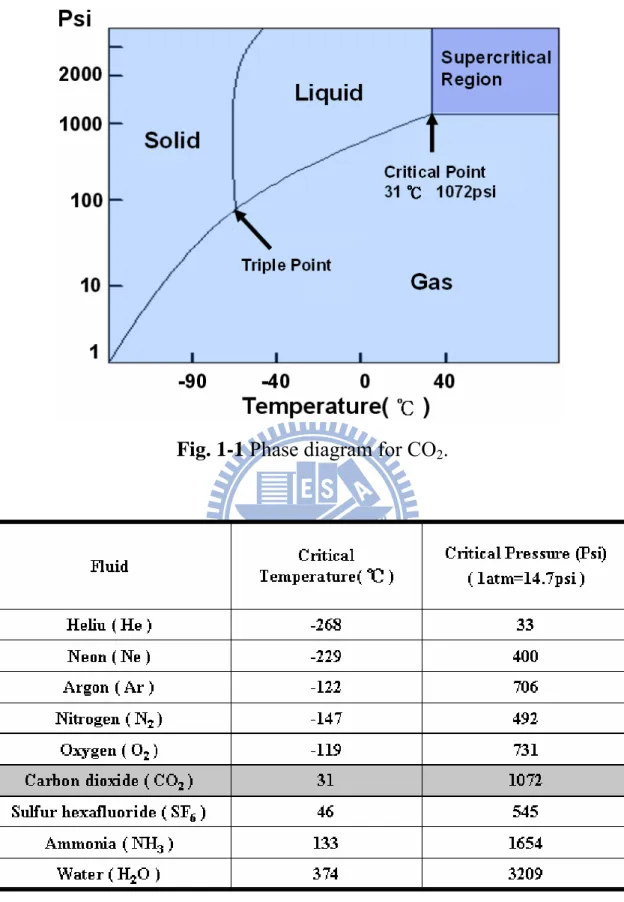
Fig. 1-1
Phase diagram for CO2.
--- 6Chaprer 2
Fig. 2-1 The supercritical fluid system. --- 13 Fig. 2-2 The experiment processes of SiO2/epi-Ge. --- 13 Fig. 2-3 Cross-sectional HRTEM images of LPCVD-SiO2 on epi-Ge substrate (a) before and (b) after the SCCO2 post-gate dielectric treatment. --- 14 Fig. 2-4 The C-V characteristics of Ge-MOS devices with various SCF treatments.
--- 14 Fig. 2-5 The projections of the phase diagram of carbon dioxide. --- 15 Fig. 2-6 XPS spectra of Ge 3d signal on the interface between gate dielectric layers
and epi-Ge before and after SCF treatment. --- 15 Fig. 2-7 The transporting mechanism for SCCO2 fluids taking H2O molecule into
dielectric film. --- 16 Fig. 2-8 C-V characteristics of 450°C PDA-treated Ge-MOS devices before and after SCCO2 post-treatment.The inset of Fig. 2-8 depicts the leakage current characteristics of the PDA-treated Ge-MOS devices before and after SCCO2 post-treatment. --- 17 Fig. 2-9 Schematic model of the mechanism of GeO desorption from the GeO2/Ge stacks. --- 18 Fig. 2-10 Direct evidence of Ge decomposition. --- 18
Chapter 3
Fig. 3-1 The experiment flows of ZrO2/GeO2 capacitor. --- 30
Fig. 3-2 The experiment flows with various SCF-liked treatments. --- 30
Fig. 3-3 EOT verses various temperatures annealing. --- 31
Fig. 3-4 Vfb verse various temperature annealing. --- 31
Fig. 3-5 Impacts with band edge photo-absorption of GeO2 films of thermal treatments on GeO2 film properties evaluated by the spectroscopic ellipsometry. --- 32
Fig. 3-6 Delta Vfb verse the various annealing temperature. --- 32
Fig. 3-7 (a) and (b) The leakage current density at the electric filed is 4×10⁶ (V/cm). --- 33
Fig. 3-8 (a) and (b) The characteristics of XRD on pure ZrO2 and ZrO2/GeO2 stacks. --- 34
Fig. 3-9 The leakage current density verse voltage before and after SCF treated. --- 35
Fig. 3-10 The Schematic diagram of Frenkel-Poole emission. --- 35
Fig. 3-11 Show the P-F fitting results to the pure ZrO2 stack at negative bias. -- 36
Fig. 3-12 Show the P-F fitting results to the ZrO2/GeO2 stacks at negative bias. --- 36
Fig. 3-13 The Schematic diagram of trap-assisted tunneling. --- 37
Fig. 3-14 Show the TAT fitting results to the pure ZrO2 stack at negative bias. - 37
Fig. 3-15 Show the TAT fitting results to the ZrO2/GeO2 stacks at negative bias. --- 38
Fig. 3-16 P-F emission Schematic diagrams. --- 40
Fig. 3-18 Capacitance verse gate voltage curve at various SCF-liked treatments.
--- 41
Fig. 3-19 Flat band voltage verses various treatments. --- 41
Fig. 3-20 Effective oxide thickness (EOT) verses various treatments. --- 42
Fig. 3-21 Hysteresis verses various treatments. --- 43
Chapter 1
Introduction
1.1 General Background
From the 1960s to current IC industry, Moore's Law is the key to lead the semiconductor industry; it’s say that the number of transistors per unit area has doubled every 18 months. That means more transistors are integrated on a chip, enabling higher performance and reduced cost. To follow Moore’s Law, the dimension of transistors must continue to be scaling down. However, as the channel length and gate oxide thickness of complementary metal oxide semiconductor (CMOS) devices continuous to shrink, short-channel effect [1] and power consumption [2] are critical problems we faced separately.
For the metal-oxide-semiconductor field-effect transistor (MOSFET), the drive current can be representation of the performance of MOSFET device, higher drive current indicate higher performance. The first order current-voltage approximation drive current in saturation region is expressed as
(
)
2 1 2 DS OX GS T W I C V V L μ = − (1-1) OX OX OX C t ε = (1-2)Where W is the channel width, L is the effective channel length, μ is the mobility of channel material, COX is the gate oxide capacitance per unit area, VGS is the voltage applied on gate to source, VT is the threshold voltage, εOX is the dielectric constant of
2
gate oxide, tOX is the gate oxide thickness. As feature size is scale down, gate length (L) and oxide thickness (tOX) shrink to lead high drive current, as scale down continuously, the above mention problems become the dramatic challenges because physical limitation of size effect. Elevating channel mobility is a way to get higher performance and avoid size issues. Enable to get high mobility for silicon based CMOS, there are two major technology; vertical structure [3,6] and channel strain [4,5] can enhance mobility of silicon channel about dozens percent [4,5]. Although the techniques can improve carrier mobility to get high performance of silicon based CMOS devices, but also face to the problems of processing is too complicated, low throughput and poor yield make cost too high. To resolve the challenges and still keep CMOS performance ongoing, a simple and intuitive way is replace silicon with new channel material.
Germanium (Ge) semiconductor has been considered as a alternative channel material in replace of Si for future high-performance CMOS technology, because its higher carrier mobility for both electrons (2.6 times) and holes (4.2 times), lower dopant thermal activation energies for shallower junction formation and compatible fabrication processes with existing silicon manufacturing infrastructure. However, the Ge-MOS technology still has many challenges and not been widely deployed. The most critical issue hindering the application of Ge is lack of high-quality and stable Ge insulation oxide comparable to silicon dioxide (SiO2) for silicon [7, 8]. The poor native Ge oxide (GeO2) layer would be soluble in water and thermally decomposed at low temperature (about 420°C) induced Ge diffuses into gate dielectric layer during the thermal deposition or post-deposition annealing (PDA) processes. The reaction of GeO2 decomposition can be expressed as
Ge+GeO2 → 2GeO(g) (1-3) Sequentially, poor interface properties and high gate leakage current will be
exhibited in the Ge-MOS device [9-13]. Various pre-gate surface modification techniques, such as surface nitridation or Si passivation, have been developed to improve the quality of gate insulator/Ge interface [14]. It was also reported that high-performance Ge MOSFET could be realized by careful control of interfacial GeO2 formation [8]. In my thesis, a low-temperature supercritical CO2 (SCCO2) fluid technology is proposed as a post-gate dielectric treatment at 150°C to improve the dielectric/Ge interface after high-temperature PDA process.
The supercritical fluid (SCF), which exists above its critical pressure and temperature, as shown in Fig 1-1 [15, 16]. It provides good liquid-like solvency and high gas-like diffusivity, giving it excellent transport capacity [17]. Table 1-1 shows critical pressure and temperature for some common fluids. CO2 is most attractive to be as supercritical fluid, because of it is easy to achieve supercritical state, low critical temperature (room temperature at 30℃) and not high critical pressure (1072psi = 72.8 atm), non-toxic, non-flammable, and inexpensive. The oxidant is also easily dissolved in SCCO2 fluid with specific surfactants. It is thereby allowed for SCCO2 fluid to transport the oxidant and penetrate the dielectric layer for trap passivation and interface oxidation at low temperature [18-20].
1.2 Motivation
To achieve a low temperature process on Ge-MOS device, high-k material is a good candidate to be gate dielectric for Germanium substrate. There are least four requirements to form gate dielectric on Germanium. First, enough high dielectric constant (>20). Second, must be thermodynamic stable with Ge, the high-k material does not react with the Ge during depositing, because a low-k interfacial layer will be form during depositing, to reduced the dielectric constant of high-k material. Third,
4
large enough band offset with Ge (>1eV), enough barrier high between Ge and gate dielectric to prevent the leakage by carriers get thermal energy to overcome the barrier between Ge and gate oxide and to create leakage. Forth, form a good interface with Ge. The hafnium oxide (HfO2) and the zirconium oxide (ZrO2) are meeting the above four conditions, and have been widely studied. For high-k metal gate, HfO2 is widely used in 45nm processing; because of it has better thermodynamic stability than ZrO2 on silicon. However, for germanium as the channel material, ZrO2 is more compatible than HfO2, because of less interfacial layer which is low k layer form after post-deposition annealing due to Ge intermixing in ZrO2 [21]. In addition, very high-k (k~37) ZrO2 have been proposed via Ge incorporation into ZrO2 [22]. Therefore, ZrO2 is a good high-k material deposited on Ge, we choose ZrO2 as our research high-k material.
Among several metal oxide films formations, in general, low temperature deposition is prefer, because of low thermal budget and low costs. However, the low-temperature deposited films have poor interfacial properties and larger leakage current due to numerous traps inside the metal oxide film. Proper annealing can reduced leakage and remove oxide charges and interface traps in the ZrO2. But for germanium substrate, the GeO2 thermal stability is a critical problem to form a good Ge-MOS. Because PDA or following high-temperature processes could induced Ge decomposition into gate dielectric, to create leakage source enhance the leakage current after annealing. On my thesis, we use the low-temperature (150℃) technique supercritical fluid (SCF) to transport the oxidant and penetrate the dielectric layer for trap passivation and interface oxidation at low temperature. And by leakage current fitting to see how leakage mechanism transfers after SCF treats.
1.3 Organization of the Thesis
In chapter 2, we first study conventional SiO2 deposited by LPCVD on epi-Germanium substrate. Discussing thermal stability and SCF treatment as deposited LP-oxide. Various analysis techniques, such as material analysis like high-resolution transmission electron microscopy (HRTEM), x-ray photoelectron spectroscopy (XPS), x-ray diffraction (XRD), were performed to characteristic the cross section of device and surface morphology. For electrical analysis, like capacitance-voltage (CV) and current density-voltage (JV) by Agilent 4980 and Keithley 4200 were perform to characteristic the device performance and analysis the interface and bulk quality of gate dielectric.
In chapter 3, we introduced the ZrO2 as high-k gate dielectric, as well as deposited GeO2 between gate insulator and Si to enlarge the GeO2 decomposition problems which lead to deterioration of the devices after post deposition annealing. Furthermore, we study the effects of SCF treatment after post dielectric annealing, by analyzing CV and JV curve which helped us to understand the recovery of Ge decomposition in Al/ZrO2/GeO2/Si capacitor before and after SCF treatment. Also, by current fitting to realize the leakage current mechanism transformation after SCF treated.
Finally, in chapter 4, gave the conclusions and suggestions of the thesis for the future work.
Fig. 1-1 Phase diagram for CO
2.
Table 1-1 Critical temperature and pressure for some common fluids.
Chapter 2
Effects of Supercritical Fluid (SCF) and Post-Deposition
Annealing (PDA) on the SiO
2
/Ge MOS Capacitor
2.1 Fabrication of Metal Oxide Semiconductor Capacitor and
Experiment Process
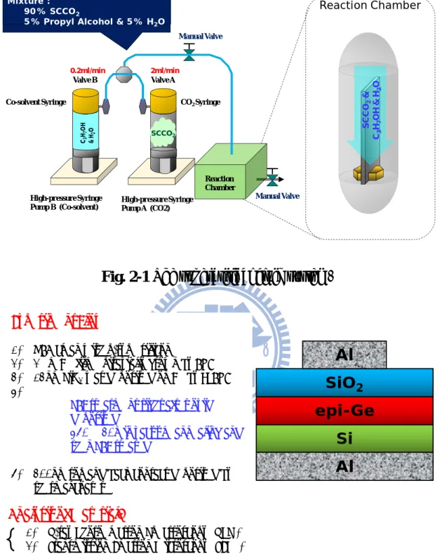
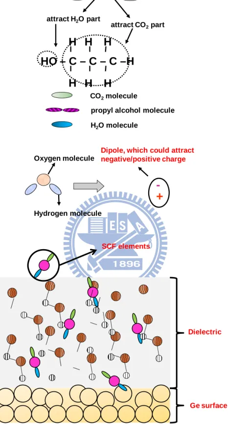
A 0.5 ohm-cm p-type (100) Si wafer was cleaned with standard RCA clean process and immediately loaded into the Applied Materials reduced-pressure chemical vapor deposition (RP-CVD) reactor. The initial 600 nm-thick Ge film was grown at 400°C with a GeH4 partial pressure of 8 Pa. Annealing under H2 ambient was then performed at 825°C for 40 min. The growth temperature was ramped to 600°C for the deposition of another 1.4 μm-thick Ge layer at 8 Pa, followed by a 15-min H2 bake at 750°C. This epitaxial Ge (epi-Ge) layer is p-type with an electrically activated concentration of 4×1015 cm-3. The wafer was immediately loaded into a low-pressure chemical vapor deposition (LPCVD) furnace with 300 mTorr and a thin silicon dioxide (SiO2) layer was deposited at 300°C on top of the epi-Ge layer, as the gate insulator of the following Ge-MOS device. It was followed that the samples were divided into two groups for study in this work. In the first group, the SCF treatment was performed right after the gate SiO2 deposition to enhance the Ge-MOS device performance. The sample was placed in a SCF system at 150°C for 1 hr, where was injected with 2000~3000 psi of SCCO2 fluid that were mixed with 5 vol.% of propyl alcohol and 5 vol.% of pure H2O. The propyl alcohol acts as a surfactant between nopolar-SCCO2 fluid and polar-H2O molecules, such that the H2O molecules are uniformly distributed in SCCO2 fluid and delivered into the gate SiO2 film to passivate defect states [28]. The supercritical fluid system is shown in Fig. 2-1.
8
In the second group, the influence of PDA on the Ge MOS device characteristics was studied further. The sample after the gate SiO2 deposition was subjected to a PDA process at 450°C for 30 min in a vacuum furnace with 1×10⁻⁷ torr, and then the SCF pos-treatment was implemented with the same conditions as mentioned above. Finally, aluminum electrodes were thermally evaporated on the top surface of SiO2 film with an electrode area of 7.07×10⁻⁴ cm2 and the back side of silicon wafer to fabricate Ge-MOS capacitors. The material analysis of X-ray photoelectron spectroscopy (XPS) on epi-Ge channel layer was also performed to examine the evolution of chemical bonding before and after SCCO2 treatment. In order to clearly distinguish the gate insulator/epi-Ge interface for signal collection, the SCCO2 process was applied to a stack structure of 13nm-thick HfO2/epi-Ge layers. It is noted that the HfO2 layer was in-situ removed by Ar+ sputtering process before XPS spectra collection. Therefore, the information of chemical bonding at the epi-Ge surface can be obtained after SCF treatment. The experiment processes of SiO2/epi-Ge capacitor with various treatments are exhibited in Fig. 2-2.
2.2 Effects of SCF on the Intrinsic SiO
2/Ge Interface
2.2.1 High-Resolution Transmission Electron Microscopy Analysis
Fig. 2-3 (a) and (b) show the cross-sectional HRTEM images of LPCVD-SiO2
on epi-Ge substrate before and after the SCCO2 post-gate dielectric treatment, respectively. In Fig. 2-3(a), the thickness of as-deposited SiO2 film is observed to be about 13.5 nm. After immersion of SCCO2 fluids with oxidant (H2O molecule) at 150°C for 1 hr, the dielectric thickness above the Ge layer is increased to about 16.6 nm in total, and a clear and even interface is exhibited, as shown in Fig. 2-3(b). It is
inferred that the increase of dielectric thickness and the even interface formed are originated from the formation of interfacial germanium oxide (GeOx) during the SCF treatment with excellent permeability. The following XPS analysis results will support the inference.
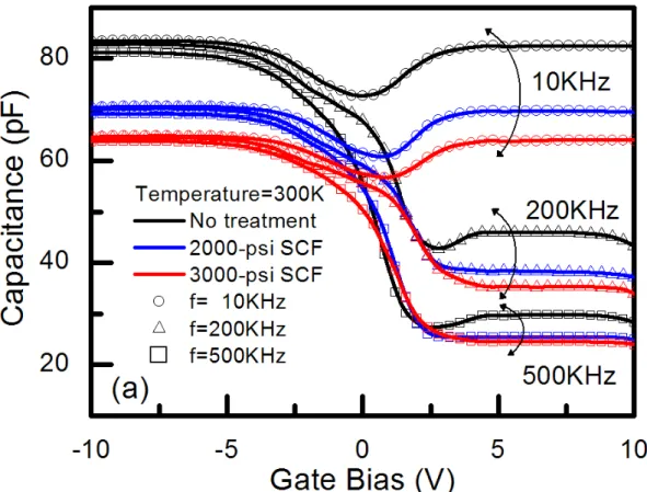
2.2.2 CV Characteristics with Various SCF Treatments
The frequency dependence of capacitance-voltage (C-V) curves for the Ge-MOS
device with various post-treatments is studied at 300K, as depicted in Fig. 2-4. It is observed that the inversion capacitance which occurs at positive gate bias for p-type Ge exhibits frequency dispersion in different levels. The frequency dispersion behavior is attributed to the response of minority carrier generation from interface defect states to measuring frequencies. The fast minority-carrier response can be achieved at low frequency [23]. Compared with the case of lower interface state densities, the Ge-MOS capacitor with higher interface state densities also will present a larger inversion capacitance, and the gap of the inversion capacitances between both cases shrinks as the increase of measuring frequencies. In this work, the inversion capacitance of Ge-MOS device with SCF treatment declines fastest and approaches to an ideal minimum capacitance as compared to the one without SCF treatment, especially in the high measuring frequency of 500 KHz. In addition, it was shown that the C-V frequency dispersion decreased with increasing the SCF pressure. It is reasonably believed that with the pressure increasing the density of CO2 will follow denser, on the other hand, the solubility of oxidant (H2O) and surfactant (propyl alcohol) are increased with increasing the CO2 pressure. Fig. 2-5 is shown the projections of the phase diagram of carbon dioxide.
10
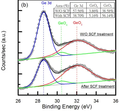
2.2.3 X-ray Photoelectron Spectroscopy (XPS) Analysis
Fig. 2-6 shows XPS spectra of Ge 3d signal on the interface between gate dielectric layers and epi-Ge before and after SCF treatment. The detected signal of Ge 3d spectra primarily comes from the surface of epi-Ge channel layer, since the gate dielectric layer was in-situ removed previously by Ar+ sputtering before XPS spectra collection. The signals of GeOx and GeO2 bonding were observed for both samples from the XPS analysis. For the sample without SCF process, it is inferred that the species of oxygen will oxidize the Ge surface to form loose native oxide layer during the early stage of gate dielectric film deposition. After SCF treatment, higher signal intensity of GeO2 bonding at the epi-Ge surface is observed obviously. The results reasonably explain that the oxidation at the gate dielectric/epi-Ge interface has occurred by adding oxidant (H2O molecules) to the SCCO2 fluid with excellent transport capacity. The formation of interfacial GeO2 layer can smoothen the epi-Ge surface and alleviate frequency dispersion of inversion capacitance.
Fig. 2-7 shows the
transporting mechanism for SCCO2 fluids taking H2O molecule into dielectric film. It shows how the SCCO2 can take oxidant (H2O) and surfactant (propyl alcohol) through the dielectric film to the dielectric/epi-Ge interface to oxidize the Germanium and passivate the defects.
2.3 The Thermal Stability and the Effects of SCF Treatment on
PDA-Treated SiO
2/epi-Ge MOS
2.3.1 Effects of the Thermal Stability on SiO2/epi-Ge Capacitor
The thermal stability and the effects of SCF treatment on PDA-treated Ge-MOS device are investigated further for realistic Ge-MOSFET fabrication consideration.
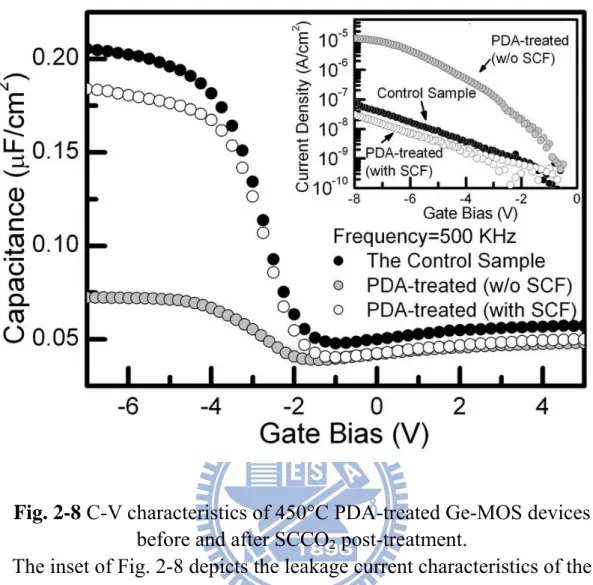
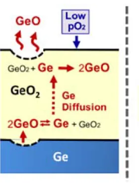
Fig. 2-8 shows C-V characteristics of 450°C PDA-treated Ge-MOS devices before and after SCCO2 post-treatment. The inset of Fig. 2-8 also depicts the leakage current characteristics of the PDA-treated Ge-MOS devices before and after SCCO2 post-treatment. The least accumulation capacitance is observed in the PDA-treated Ge-MOS device, about a 66% reduction compared with the control sample (without PDA process). The significant reduction of the accumulation capacitance due to poor charge holding capability can be attributed to the large leakage current of PDA-treated Ge MOS device, as shown in the inset of Fig. 2-8. It was reported that thermal process induces Ge decomposition and desorption into gate dielectric layer. Fig. 2-9 and Fig. 2-10 shows the mechanism of Ge decomposition with the GeO2 which stacks on the Ge, after high temperature annealing, and the direct evidence GeO2 desorption and consume the Ge substrate cause extremely uneven surface [24]. Also, the incorporation of Ge in dielectric insulator is believed to act as defect traps and thereby causes an increased gate leakage current [8, 11, 14].
2.3.2 Effects of SCF Treatment on PDA-Treated Ge-MOS
In this study, the implementation of SCF treatment after PDA process
significantly reduces leakage current of gate insulator and recovers the C-V characteristic to a similar state as the initial Ge-MOS device without PDA process (control sample). This indicates again that oxidant (H2O molecule) is effectively transported into SiO2 film by the high-pressure SCF and passivates the defect states generated in the Ge-MOS device during high-temperature thermal PDA process.
12
2.4 Summary
In summary, a low-temperature SCCO2 process at 150°C has been proposed to treat the gate oxide/epi-Ge interface and restore Ge-MOS device degradation after a high-temperature PDA process. It is observed that the uneven and poor interface was easily formed during thermal deposition processes on epi-Ge layer. After the SCF treatment, a smooth GeO2 interface layer is formed and the frequency dispersion of inversion capacitance is alleviated. Furthermore, electrical degradation of Ge-MOS device after 450°C PDA process leads to the reduction of accumulation capacitance and the increase of gate leakage current. The SCF treatment also can transport the oxidant into the gate dielectric layer and passivate the Ge-related defect states generated by PDA process. Electrical characteristics of Ge-MOS device are effectively recovered to an extent similar to the one before PDA process.
High-pressure Syringe Pump B (Co-solvent)
Co-solvent Syringe CO2 Syringe
Reaction Chamber Manual Valve Manual Valve High-pressure Syringe Pump A (CO2) Valve B Valve A Reaction Chamber Mixture : 90% SCCO2
5% Propyl Alcohol & 5% H2O
S CCO 2 & C3 H7 OH & H2 O SCCO2 C3 H7 OH & H 2 O 0.2ml/min 2ml/min
Fig. 2-1 The supercritical fluid system.
Si
epi-Ge
SiO
2Al
Al
Experiment Flow Analysis of Material: 1. RCA clean with p‐type silicon2. 2 μm Ge film epitaxially grown by CVD 3. 13nm SiO2was deposited on Ge by LPCVD
4. SCF treatment right after oxide deposited 450℃ 30min vacuum annealing and then SCF treated 5. 300nm top and back contact deposited by thermal coater 1. X‐ray Photoelectron Spectroscopy (XPS). 2. Transmission Electron Microscopy (TEM). 1. Current density‐electric field (J‐E) characteristics. 2. Capacitor‐voltage (C‐V) characteristics. Analysis of Electrical characteristics:
Fig. 2-3 Cross-sectional HRTEM images of LPCVD-SiO2 on epi-Ge
substrate (a) before and (b) after the SCCO
2post-gate dielectric treatment
Fig. 2-4 The C-V characteristics of Ge-MOS devices with various SCF
treatments.
Fig. 2-5 The projections of the phase diagram of carbon dioxide.
Fig. 2-6 XPS spectra of Ge 3d signal on the interface between gate
dielectric layers and epi-Ge before and after SCF treatment.
CO2molecule H2O molecule attract H2O part attract CO2part
HO – C – C – C –H
H
H
H
H
H
H
propyl alcohol molecule
Oxygen molecule
Hydrogen molecule
+
-Dipole, which could attract negative/positive charge 16
Dielectric Ge surface SCF elements
Fig. 2-7 The
transporting mechanism for SCCO
2fluids taking H
2O
molecule into dielectric film.
Fig. 2-8 C-V characteristics of 450°C PDA-treated Ge-MOS devices
before and after SCCO
2post-treatment.
The inset of Fig. 2-8 depicts the leakage current characteristics of the
PDA-treated Ge-MOS devices before and after SCCO
2post-treatment.
Fig. 2-9 Schematic model of the mechanism of GeO desorption from the
GeO
2/Ge stacks.
Fig. 2-10 Direct evidence of Ge decomposition
Chapter 3
Effects and mechanisms of PDA and following SCF
treated on the ZrO
2/GeO
2/Si MOS capacitor
3.1 Fabrication of ZrO
2/GeO
2Stack with MOS Capacitor and
Experiment Process
A 0.5 ohm-cm p-type (100) Si wafer was cleaned with standard RCA clean process and immediately loaded into the E-gun evaporator chamber. As the chamber pressure reached to the 5×10⁻⁶ torr, heater was opened and temperature was setting on 250°C. At the temperature was achieved to the 250°C, the initial 1nm GeO2 film was grown at 250°C by E-gun evaporator, 20 min temperature holding after deposition was completed. Turn the heater off and waiting for 1 hr let chamber temperature to cold down to room temperature. In situ., opened the heater to reach to 250°C, the second 10nm ZrO2 film was grown at 250°C by E-gun evaporator, 20 min temperature holding after deposition was completed. Turn the heater off, and waiting temperature cold down to the room temperature. The sample was subjected to the post deposition annealing, under 400°C and 500°C 30min in a vacuum furnace, 600°C 30sec. in a rapid temperature annealing (RTA), separately. The SCF treatment was performed right after the PDA to repair the device performance. The sample was placed in a SCF system at 150°C for 1 hr, where was injected with 2500 psi of SCCO2 fluid that were mixed with 5 vol.% of propyl alcohol and 5 vol.% of pure H2O. Finally, 500nm aluminum electrodes were thermally evaporated on the top surface of ZrO2 film with an electrode area of 7.07×10⁻⁴ cm2 and the back side of silicon wafer to
fabricate MOS capacitors. The IV and CV curve to see the MOS-capacitor properties, and by current fitting to comprehend the mechanism of Ge-related defects enhancing the leakage. The experiment flows of ZrO2/GeO2 capacitor with various treatments are exhibited in Fig. 3-1.
Second part, we want to see the effects of independent SCCO2 and H2O treatment on ZrO2 thin films, to confirm the validity after SCF treated on the ZrO2 films. A 0.5 ohm-cm p-type (100) Si wafer was cleaned with standard RCA clean process. 10nm ZrO2 deposited on Si immediately by E-gun evaporator, and then there are high pressure treating after dielectric depositing. Finally, 500nm aluminum electrodes were thermally evaporated on the top surface of ZrO2 film with an electrode area of 7.07×10⁻⁴ cm2 and the back side of silicon wafer to fabricate MOS capacitors. The IV and CV curve to see the MOS-capacitor properties. The experiment flows with various SCF-liked treatments are exhibited in Fig. 3-2. The results will show in section 3.4.
3.2 Effects of PDA on the ZrO
2/GeO
2/Si MOS Capacitor
3.2.1 Parameter Description
There are three parameters represent the characteristics of MOS capacitors.
¾ Effective Oxide Thickness (EOT)
(3-1) 2 2 . SiO ZrO ox thick A A C EOT d ε ε = = 2 2 . SiO thick ZrO EOT ε d ε = (3-2) 20
Eq. (3-2) represents the effective oxide thickness (EOT) related to the dielectric constant of ZrO2. For the Eq. (3-2), the less EOT represents the value of k is higher. Where εSiO2 is dielectric constant of SiO2, εZrO2 is dielectric constant of ZrO2, dthick is thickness of ZrO2.
¾ Flat Band Voltage (Vfb)
o FB ms ox Q V C φ = − (3-3)
Eq. (3-3) represents the number of charge exists inside the dielectric, that means the Vfb near the zero bias, the less oxide charges existing inside the dielectric. Where φms is the work function difference between gate and substrate, Q0 is the number of oxide charges in the dielectric.
¾ Hysteresis (△Vfb)
Hysteresis represents the quality of interface between the dielectric and substrate, smaller △Vfb indicate better interface quality.
3.2.2 Characteristics of CV and IV Curves
Fig. 3-3 indicate the EOT verses various temperatures annealing. The dark
square is pure ZrO2 stack on Si. The red square is ZrO2/GeO2 stacks on Si. As annealing temperature increasing, the EOT is shrinking; represent the higher k values of ZrO2 along with temperature increasing. At 500~600°C we can find the good annealing temperature. But at higher temperature annealing (> 600°C), the EOT uplift due to the low k interfacial layer have been formed.
Fig. 3-4 is shown the Vfb verse various temperature annealing. For pure ZrO2 stack, the Vfb reduced along with annealing temperature increased, the PDA treatment can effective remove the oxide charges in the high-k films. For ZrO2/GeO2 stacks, the
22
Vfb generally reduced with temperature increased, expect the 400°C condition, the Vfb shift to the negative is due to the Ge2+ typed defects creation [24]. Fig. 3-5 shows the impacts with band edge photo-absorption of GeO2 films of thermal treatments on GeO2 film properties evaluated by the spectroscopic ellipsometry. From the literature, it indicates the tailing states formation at the GeO2 band edge after annealing. Because of Ge decomposition or GeO desorption enhanced the oxygen-deficiency in GeO2 films to induce the defects like neutral oxygen vacancy or Ge2+, cause the Vfb shift to the negative bias [24,25].
Fig. 3-6 shows the delta Vfb verse the various annealing temperature. No matter the pure ZrO2 or ZrO2/GeO2 stacks, the hysteresis can effectively be reduced via PDA, showing the appropriate annealing can improve the interface quality.
Fig. 3-7 (a) and (b) show the leakage current density at the electric filed is 4×10⁶ (V/cm). We separate tow parts to discuss, the positive and negative bias. For the positive bias, the electron-hole pairs are generated by thermal excitation in deep depletion region to as leakage source. The current is limited by generation rate of minority carriers. Also, the traps near the interface contribute to the saturation current. So the interface quality will affect the leakage current of positive bias, the current increases with the number of density of interface traps in the interface [26]. Fig. 3-7 (a) for pure ZrO2, the leakage of positive bias is reducing with annealing temperature increasing; show the density of interface traps can be improved by proper PDA. The results also correlated the characteristic of hysteresis. However, for ZrO2/GeO2 stacks, the different trend was observed relative to the pure ZrO2. Which along with temperature increasing the current density also increasing are due to Ge decomposition causing interface deterioration. The Ge decomposition makes interface consumption and creates interface traps to provide a path for minority carrier generation.
Fig. 3-7 (b) shows the leakage at negative bias. The leakage can be reduced through the modified temperature annealing. Above 600°C, the leakage is increased due to the complete poly-crystallization; the grain boundary supply a path of the leakage, on the other hand, the carrier will follow grain boundaries to form the leakage paths. The characteristics of XRD were show the crystal pattern in Fig. 3-8 (a) and (b). From the XRD, we can see as deposited the ZrO2 film is amorphous, along with annealing temperature increased; the peak of XRD is more significant, which shows the more complete crystallizing after 600°C annealing. But for the ZrO2/GeO2 stacks, after 600°C annealing, the leakage current increase dramatically, it would not only due to ZrO2 crystallization but also the Ge decomposition makes the GeO diffusion into the dielectric to enhanced the leakage uplift.
3.3 Leakage Mechanism Transferred After Post-SCF Treated
3.3.1 Characteristics of JV Curves
Fig. 3-9 is show the leakage current density verse voltage before and after SCF
treated which the dielectric after 600°C N2 30sec. RTA annealing. The circle points represent the pure ZrO2 stack. The triangle points represent the ZrO2/GeO2 stacks. For the pure ZrO2 after 600°C annealing, the leakage is uplift. It was attributed to the crystallization of ZrO2 films. When the post-SCF treatment applied, there is the not obvious difference between before and after SCF treated. We speculate that the SCF treatment could not repair the defect which creation is due to the grain boundary by high temperature annealing. According to the reference, it proposes there are defects existing in the grain boundary; some of the defects are shallow traps, which cause leakage current increasing [27]. For the ZrO2/GeO2 stacks, the significant leakage
current increase by 600°C annealing, in addition to the crystallization by annealing, the main reason may be the GeO2 decomposition makes the dielectric deterioration by Ge or GeO diffusion into the ZrO2 films to cause Ge-related defects or neutral oxygen vacancy to enhance the leakage. As applied the SCF treatment, the leakage can be effectively reduced. Showing the SCF treated have the capacity of improving the dielectric which degradation by GeO2 decomposition. We inference that the SCF can remove Ge-typed defects to reduced leakage after post-deposition annealing. The next section, by current fitting, we will clarify the leakage mechanism transformation after annealing and following SCF treating. To investigate how GeO2 decomposition makes the gate leakage current increasing in Ge-related devices.
3.3.2 Conduction Mechanisms
There are many conduction mechanisms in the insulator thin films, including Schottky-Richardson emission [29], Frenkel-Poole emission [29,30], Fowler-Nordheim tunneling [29,30], and trap assisted tunneling [31,32]. Among the mechanisms, the Frnkel-Poole emission (PF) and trap-assisted tunneling (TAT) are most widely used to explain the leakage mechanisms in high-k thin films. The Frenkel-Poole emission is due to field-enhanced thermal excitation of trapped electrons in the insulator into the conduction band. Fig. 3-10 is show the Schematic diagram ofFrenkel-Poole emission. The leakage current equation as following is
(3-4) exp t PF B qE q J CE k T φ πε ⎡− ⎛ − ⎞⎤ ⎢ ⎜⎝ ⎟⎠⎥ ⎢ ⎥ = ⎢ ⎥ ⎢ ⎥ ⎣ ⎦ 24
Where C is the constant, E is the applied electric field, q is the electronic charge, φt is the trap barrier high, ε is the dielectric constant, Tis the absolute temperature, and
is the Boltzmann constant. Arrange the eq. 3-4, the intercept and slope can be determined from B k ln( )J E versus 1/2
E plots. The intercept and slope are show
t B q Intercept k T φ − = (3-5) B q Slope k T πε = (3-6)
The trap barrier high (φt) is the depth of the trap potential well, can be extracted from intercept which determined from the ln( )J
E versus
1/2
E plots by Frenkel-Poole
emission equation. Fig. 3-11 and Fig. 3-12 show the fitting results for the pure ZrO2 and ZrO2/GeO2 stacks separately at negative bias. It’s good linear fitting at the higher electric filed range. A good linear fitting explains the leakage current in higher electric filed indeed leakage by Frenkel-Poole emission.
The other dominant leakage mechanism is the trap-assisted tunneling (TAT). It is assumed that electrons first tunnel into the ZrO2 (direct-tunneling) by the traps existing into the insulator. Then, electrons tunnel through traps located below the conduction band of the high-k thin film by Fowler-Nordheim tunneling [1] and direct tunnel [1,33] through the GeOx layer to the substrate. Fig. 3-13 is show the Schematic diagram of trap-assisted tunneling. The leakage current equation is
3 2 8 2 * exp 3 TAT t qm J A hE π φ ⎛− ⎞ = ⎜ ⎟ ⎝ ⎠ (3-7)
in the ZrO2 (m* = 0.3m0 [28]), m0 is the free electron mass, h is the Planck constant, E is the applied electric filed, φt is the trap barrier high. Also the trap barrier high (φt) is the depth of the trap potential well, can be extracted from slope which determined from the ln versus J 1
E plots by trap-assisted tunneling equation. The slop is
showing as 3 2 8 2 * 3 t qm Slope h π φ − = (3-8)
Fig. 3-14 and Fig. 3-15 show the good linear fit for the pure ZrO2 and ZrO2/GeO2 stacks separately at the lower electric filed. A good linear fitting explains the leakage current in lower electric filed indeed leakage by trap-assisted tunneling emission. The fitting results and extraction parameters will on the Table 3-1, 3-2, 3-3 and 3-4. For the pure ZrO2 stack, is shown in the Table 3-1 and 3-2, after 600°C N2 30sec. annealing, we can find that the leakage is increasing. By current mechanism fitting, we observe the shallow traps creation via poly-crystallization at high temperature annealing. The result is consistent with the literature [27]. When applied the SCF treatment after annealing, the trap barrier high did not change, so the leakage couldn’t be suppressed by SCF treating. The shallow traps creation enhanced the leakage current, because of more leakage paths can be form by carrier easily passing through the insulator via shallow traps no matter what P-F emission and TAT tunneling. For Poole-Frenkel emission, as trap barrier get higher, fewer electrons can get enough thermionic energy to overcome the barrier to the substrate. Schematic diagram is shown in Fig. 3-16. For trap-assisted tunneling, as trap barrier get shallower, more electrons at traps in the ZrO2 can easily tunnel by Fowler-Nordheim tunneling to the conduction band at low electric filed. As trap barrier get deeper, lager electric filed is
need to apply, let barrier changing to triangle barrier to tunnel. Schematic diagram is shown in Fig. 3-17.
For the ZrO2/GeO2 stacks, is shown in the Table 3-3 and 3-4, after 600°C N2 30sec. annealing, the leakage current significantly increasing, the results also show in Fig. 3-9. From current mechanism fitting, we similarly observe that the shallow traps creation by high temperature annealing. As mention above, the leakage uplift obviously would be due to the poly-crystallization and GeO2 decomposition. However, after SCF treatment, we see that the leakage can be effectively reduced and traps barrier are changing to higher. So we realize that the GeO2 decomposition causing the Ge or GeO diffusion into the ZrO2 thin films to create the Ge-related defects. These defects are shallow traps; enhance the leakage by P-F emission and TAT. From fitting results in Table 3-3 and 3-4, the trap barrier high were recover from shallower barrier to the deeper barrier, and the gate leakage current also can be reduced. We deduce that the SCF treatment could remove the shallow traps by GeO2 decomposition but not obviously reduce the shallow traps which create by poly-crystallization.
3.4 Various SCF-liked Treatments on ZrO
2Thin Films
The Fig. 3-18 is shown the capacitance verse gate voltage curve at various treatments. From the CV curve, we find that after the treatments, the flat band voltage shift to the zero bias, indicate that the oxide charges inside the gate insulator were removed after SCF-liked treatments. However, for various treatments, there are not obvious differences between the treatments. We arrange the flat band voltage verse various treatments at Fig. 3-19, its clear show that the results are consistent with CV curve. The Fig. 3-20 is showed the effective oxide thickness (EOT) verse various treatments. It shows that the EOT reduced slightly after treatments, and we use
28
NK1200 to measure physical thickness and extract the dielectric constant, the results show in Table 3-5. The ZrO2 after SCF-liked treatments the k values are uplift slightly, we speculate that it could be due to the temperature effect, because the SCF-liked treatments all operating at 150°C. Fig. 3-21 is shown the hysteresis verses various treatments and Fig. 3-22 is shown the current density verse voltage under various SCF-liked treatments. There are not obviously difference between the various treatments and control sample. According to the results, we consider whether the vapor annealing at 150°C, or only SCCO2 without the co-solvent at 150°C , or the SCCO2 with co-solvent at 150°C, ZrO2 thin films is not sensitivity with SCF treatments, the temperature may be more critical for high-k films.
3.5 Summary
In this study, the modified post-deposition annealing is necessary to form the
good gate dielectric insulator by low temperature deposition (E-gun evaporator was used in my thesis). The EOT, flat band voltage and hysteresis were reduced by PDA, showing the annealing can improve the quality of gate dielectric and remove the defects which thin films as-deposited at low temperature. At 600°C annealing, the leakage uplift is due to the ZrO2 poly-crystallization, the results are show in XRD. Then we deliberately form 1nm GeO2 thin films between the ZrO2 and Si to enlarge the GeO2 formation as insulator depositing on germanium substrate. The significantly degradation of MOS properties are observed after 600°C annealing, comparing the pure ZrO2 stack, we realized that the GeO2 decomposition makes Ge diffusion or GeO desorption to produce the shallow traps which enhance the leakage as annealing temperature increased. A low temperature treatment (at 150°C) was applied after PDA is successfully employing to improve the Ge-related devices. The supercritical fluids
technology have capacity of carrying the oxidant (H2O) and surfactants (propyl alcohol) into the E-gun-deposited ZrO2 thin films to remove the shallow traps and passivate surface states which are Ge-related defects by thermal decomposition at low temperature. For various SCF-liked treatments there are not obviously difference between the various treatments and control sample. So we simple to the conclusion, ZrO2 thin films is not sensitivity with SCF treatments, the temperature may be more critical for high-k films which deposited at low temperature.
Experiment Flow Analysis of Electrical characteristics: 1. RCA clean with p‐type silicon 2. 1nm GeO2was deposited on Si by E‐gun evaporator at 250 ℃ 3. 10nm ZrO2was deposited on Si by E‐gun evaporator at 250 ℃ 4. The MOS stack structure ZrO2/Si
ZrO2/GeO2/Si
5. Various PDA treatment 400 ℃ 30min by vacuum furnace 500 ℃ 30min by vacuum furnace 600 ℃ 30 sec. N2by RTA 6. 2500psi 1hr SCF treatment after PDA 7. 500nm top and back contact deposited by thermal coater 1. Capacitor‐voltage (C‐V) characteristics. 2. Current density‐electric field (J‐E) characteristics. 3. Leakage current mechanism fitting at negative bias. 30
Fig. 3-1 The experiment flows of ZrO
2/GeO
2capacitor.
Fig. 3-2 The experiment flows with various SCF-liked treatments.
Si
Al
ZrO
2GeO
2Al
Experiment Flow Analysis of Electrical characteristics: 1. RCA clean with p‐type silicon 2. 10nm ZrO2was deposited on Si by E‐gun evaporator at 250 ℃ 3. Various SCF‐liked treatment 150 ℃ 1hr vapor annealing 2500 psi 150 ℃ 1hr pure SCCO2 treatment 2500 psi 150 ℃ 1hr pure SCCO2+colvent 4. 500nm top and back contact deposited by thermal coater 1. Capacitor‐voltage (C‐V) characteristics. 2. Current density‐voltage (J‐V) characteristics.Si
Al
ZrO
2Al
Characteristics of EOT under PDA treated
STD 400F 500F 600RTA EO T (A ) 30 40 50 60 70 80 90 ZrO2@250C ZrO2/GeO2@250C
Fig. 3-3 EOT verses various temperatures annealing.
Characteristics of Vfb under PDA treated
STD 400F 500F 600RTA Vfb (V ) -4.0 -3.5 -3.0 -2.5 -2.0 -1.5 -1.0 -0.5 ZrO2@250C ZrO2/GeO2@250C
Fig. 3-5 Impacts with band edge photo-absorption of GeO
2films of
thermal treatments on GeO
2film properties evaluated by the
spectroscopic ellipsometry.
Characteristics of ΔVfb under PDA treated
STD 400F 500F 600RTA Δ Vfb (V ) -0.5 0.0 0.5 1.0 1.5 2.0 ZrO2@250C ZrO2/GeO2@250C
Fig. 3-6 Delta V
fbverse the various annealing temperature.
32Jg @ E=4x10 6 (V/cm) STD 400F 500F 600RTA Cur re nt density (A m p/cm 2 ) 1e-8 1e-7 1e-6 1e-5 1e-4 ZrO2@250C ZrO2/GeO2@250C Positive bias
(a)
Jg @ E= - 4x10⁶(V/cm) STD 400F 500F 600RTA Cur re nt density (A m p/cm 2 ) 1e-7 1e-6 1e-5 1e-4 1e-3 1e-2 1e-1 1e+0 ZrO2@250C ZrO2/GeO2@250C Negative bias(b)
Fig. 3-7 (a) and (b) The leakage current density at the electric filed is
4×10
6(V/cm)
XRD@pure ZrO2 Angle(2θ) 30 35 40 45 50 55 60 65 Inte nsi ty (a. u.) 100 200 300 400 500 600 700 800 STD 400C@30min 500C@30min 600C@30sec
t(101)
t(112)
t(211)
t(110)
(a)
XRD@ZrO2/GeO2 Angle(2θ) 30 35 40 45 50 55 60 65 Inte nsi ty (a. u.) 100 200 300 400 500 600 700 800 900 STD 400C@30min 500C@30min 600C@30sect(101)
t(110)
t(112)
t(211)
(b)
Fig. 3-8 (a) and (b) The characteristics of XRD on pure ZrO
2and
ZrO
2/GeO
2stacks.
Characteristics of JV
Volt(V) -4 -2 0 2 4 Cur re nt densit y (A m p/cm 2 ) 1e-10 1e-9 1e-8 1e-7 1e-6 1e-5 1e-4 1e-3 1e-2 1e-1 1e+0 1e+1 STD@ZrO2 600R 600R+SCF STD@ZrO2/GeO2 600R 600R+SCFFig. 3-9 The leakage current density verse voltage before and after SCF
treated.
Al
ZrO
2Si
“-” bias
GeOxe
Poole-Frenkel emission @pure ZrO2 (neagative bias)
E1/2(MV/cm)1/2 500 1000 1500 2000 2500 3000 3500 J/E (A /c m -V) -32 -30 -28 -26 -24 -22 -20 STD 600C for 30sec 600C+SCF
PF@pure ZrO
2Fig. 3-11 Show the P-F fitting results to the pure ZrO
2stack at negative
bias.
Poole-Frenkel emission @ZrO2/GeO2 (neagative bias)
E1/2(MV/cm)1/2 500 1000 1500 2000 2500 J/ E( A /c m -V ) -32 -28 -24 -20 -16 STD 600C for 30sec 600C+SCF
PF@pure ZrO
2/GeO
2
Fig. 3-12 Show the P-F fitting results to the ZrO
2/GeO
2stacks at negative
bias.
Al ZrO2 Si “-” bias GeOx e
-Fig. 3-13 is show the Schematic diagram of trap-assisted tunneling.
Trap-Asisted tunneling @pure ZrO2 (neagative bias)
1/E(cm/MV)
1.0e-7 2.0e-7 3.0e-7 4.0e-7 5.0e-7
J(A /c m 2 ) -18 -16 -14 -12 -10 -8 -6 -4 STD 600C for 30sec 600C+SCF
TAT@pure ZrO
2Fig. 3-14 Show the TAT fitting results to the pure ZrO
2stack at negative
bias.
Trap-Asisted tunneling @ZrO2/GeO2 (neagative bias)
1/E(cm/MV)
2e-7 3e-7 4e-7 5e-7
J(A /cm 2 ) -16 -12 -8 -4 0 STD 600C for 30sec 600C+SCF
TAT@pure ZrO
2/GeO
2Fig. 3-15 Show the TAT fitting results to the ZrO
2/GeO
2stacks at
negative bias.
Slope×10-3(A/cm1/2*V3/2) Intercept(A/cm*V) Trap barrier(eV)
STD 10 -50.27 1.30
600R 5.39 -38.80 1.00
600R+SCF 5.51 -38.89 1.01
Poole-Frenkel
Table 3-1 Pure ZrO
2parameters extraction by P-F emission fitting.
Slope×107 Trap barrier(eV)
STD -4.54 1.14
600R -1.44 0.53
600R+SCF -1.47 0.54
Trap assisted
Table 3-2 Pure ZrO
2parameters extraction by TAT fitting.
Slope×10-3(A/cm1/2*V3/2) Intercept(A/cm*V) Trap barrier(eV)
STD 9.44 -44.89 1.16
600R 5.32 -28.86 0.73
600R+SCF 7.62 -42.35 1.10
Poole-Frenkel
Table 3-3 ZrO
2/GeO
2parameters extraction by P-F emission fitting.
Slope×107 Trap barrier(eV)
STD -2.94 0.85
600R -1.18 0.46
600R+SCF -1.88 0.63
Trap assisted
Al
ZrO
2
Si
“-” bias
GeO
x
e
-Easier
Fig. 3-16 P-F emission Schematic diagrams
Al
ZrO
2
Si
“-” bias
GeO
x
e
-Low filed
Fig. 3-17 TAT Schematic diagrams.
CV@ZrO2 under various SCF-liked treatments Volt(V) -4 -3 -2 -1 0 1 2 Cp apcit ance( F) 0.0 5.0e-10 1.0e-9 1.5e-9 2.0e-9 STD 2500psi @SCCO2 vapor STD_SCF
Fig. 3-18 Capacitance verse gate voltage curve at various SCF-liked
treatments.
Vfb@ZrO2 under various SCF-liked treatments STD 2500psi vapor STD_SCF Vfb (V ) -1.9 -1.8 -1.7 -1.6 -1.5 -1.4
Fig. 3-19 Flat band voltage verses various treatments.
EOT@ZrO2 under various SCF-liked treatments STD 2500psi vapor STD_SCF EOT (A ) 40 42 44 46 48 50
Fig. 3-20 Effective oxide thickness (EOT) verses various treatments.
non 2500psi vapor STD_SCF
Initial k 10.5
After k 11.88 11.57 11.45
Table 3-5 The dielectric constants under various SCF-liked treatments.
ΔVfb@ZrO2 under various SCF-liked treatments STD 2500psi vapor STD_SCF Δ Vfb (V ) 0.4 0.6 0.8 1.0 1.2 1.4 1.6
Fig. 3-21 Hysteresis verses various treatments.
JV@ZrO2 under various SCF-liked treatments Volt(V) -4 -2 0 2 4 Cur re nt de nsi ty (A m p/ c m 2 ) 1e-9 1e-8 1e-7 1e-6 1e-5 1e-4 1e-3 STD 2500psi @SCCO2 vapor STD_SCF
44
Chapter 4
Conclusions and Suggestions for Future Work
4.1 Conclusions
In this study, we originally and successfully employ the supercritical CO2 fluids technology to apply the Ge-typed MOS devices. A low-temperature SCCO2 process at 150°C has been proposed to treat the LPCVD-SiO2/epi-Ge interface and restore Ge-MOS device degradation after a high-temperature PDA process. A smooth GeO2 interface layer is formed and the frequency dispersion of inversion capacitance is alleviated after PDA process. Furthermore, electrical degradation of Ge-MOS device after 450°C PDA process leads to the reduction of accumulation capacitance and the increase of gate leakage current. The SCF treatment also can passivate the Ge-related defect states generated by PDA process. Electrical characteristics of Ge-MOS device are effectively recovered to an extent similar to the one before PDA process.
The modified post-deposition annealing is necessary to form the good high-k films by low temperature deposition (E-gun evaporator was used in my thesis). At 600°C annealing, the leakage uplift is due to the ZrO2 poly-crystallization, and for the GeO2 stack in the MOS devices the leakage will be enhanced obviously. The low temperature (at 150°C) supercritical fluid can effectively improve the MOS devices to remove the shallow traps by thermal decomposition of GeO2 via high temperature annealing.
The supercritical fluid is the low temperature and attractive technology to apply on Ge-typed MOS devices process. It’s useful to resolve the GeO2 thermal issues to fabricate the high quality Ge-typed MOS devices at low-temperature.
4.2 Suggestions for Future work
To complete the high quality Ge-MOSFET, metal gate is another issue on the
germanium devices. The work function tuning is a key to determined threshold voltage, however, for Ge-MOSFET, Fermi level pinning is the problem on metal gate/ high-k/Ge MOS stack devices, which is waiting to be solved.
The feasibility of SCF nitridation is interesting topic on fabricated Ge-MOSFET processing; because of this is the low temperature process relative to the plasma ntridation or high temperature furnace annealing. Alter the co-solvent from H2O to the NH3 to see the probability of SCF nirtidation.
46
Reference
[1] S. M. Sze, and Kwok K. Ng, Physics of Semiconductor Devices 3rd. [2] E. J. Nowak, IBM J. Res. & Dev. Vol. 46 No. 2/3, 2002.
[3] K. Rim, S. Koester, M. Hargrove, J. Chu, P. M. Mooney, J. Ott,T. Kanarsky, P.Ronsheim, M. Ieong, A. Grill, and H.-S. P. Wong, Symposium on VLSl
Technology Digest of Technical Papers, pp.59-60, 2001.
[4] M. L. Lee, Eugene A. Fitzgerald, Mayank T. Bulsara, Matthew T. Currie, and Anthony Lochtefeld, J. Appl. Phys. Vol. 97, 011101, 2005
[5] Scott E. Thompson, Robert S. Chau, Tahir Ghani, Kaizad Mistry, Sunit Tyagi, and Mark T. Bohr, IEEE T. Semiconduct. M. Vol. 18, No. 1, pp. 26, 2005
[6] X. Huang, W.-C. Lee, C. Kuo, D. Hisamoto, L. Chang, J. Kedzierski, E. Anderson, H. Takeuchi, Y.-K. Choi, K. Asano, V. Subramanian, T.-J. King, J. Bokor, and C. Hu, “Sub 50-nm FinFET: PMOS,” IEEE T. Electron Dev. Vol. 48,
No. 5, pp. 880, 2001
[7] S. Takagia, T. Maeda, N. Taoka, M. Nishizawa, Y. Morita, K. Ikeda, Y. Yamashita, M. Nishikawa, H. Kumagai, R. Nakane, S. Sugahara and N. Sugiyama,
Microelectron. Eng. Vol. 84, pp.2314, 2007.
[8] Hiroshi Matsubara, Takashi Sasada, Mitsuru Takenaka, and Shinichi Takagi, Appl.
Phys. Lett. Vol. 93, 032104, 2008.
[9] K. Prabhakaran, F. Maeda, Y. Watanabe, and T. Ogino, Appl. Phys. Lett. Vol. 76,
2244, 2000.
[10] J. Oh and J. C. Campbell, J. Electron. Mater. Vol. 33, pp.364, 2004.
[11] S. Van Elshocht, B. Brijs, M. Caymax, T. Conard, T. Chiarella, S. De Gendt, B. De Jaeger, S. Kubicek, M. Meuris, B. Onsia, O. Richard, I. Teerlinck, J. Van