© 2012 The Electrochemical Society. [DOI:10.1149/2.012206jss] All rights reserved.
Manuscript submitted April 23, 2012; revised manuscript received August 17, 2012. Published October 2, 2012.
Semiconducting polymers are attractive because they can be pro-cessed easily on a large-scale flexible substrate at a low processing temperature and at low cost. Solution-processable, self-organized, re-gioregular poly(3-hexylthiophene) (P3HT) is suitable for fabricating organic thin-film transistors (OTFTs) because of their high carrier mobility. OTFTs with a P3HT active layer (i.e., PTFTs) have demon-strated high hole mobility (0.01–0.3 cm2/V s), with a reasonable on/off
ratio (more than 100 in air and 106in an inert atmosphere).1–3 Stud-ies have attempted to improve their performance by enhancing the crystallinity of the P3HT layer through various techniques, such as changing solvents, modifying coating methods, and/or incorporating thermal annealing.3–6Other than improving crystallinity, the dopant concentration in the P3HT and the injection barrier between P3HT and the electrodes can also be modified by thermal annealing.3,7–10Recent studies have proposed a correlation between the characteristics of PTFTs and the thickness of the active layer.11–13This correlation was attributed to the existence of bulk current in the active layer before the formation of the accumulation layer, and a higher bulk current is usually conducting in a thicker active layer.11,12 Moreover, poor off-current and subthreshold swing were observed when the thick-ness of the active layer was increased.11,12 Therefore, based on this knowledge, this study developed an innovative technique that can dramatically improve the performances.
In this study, a systematic investigation was conducted on new de-vices with double-coated channel layers (DPTFTs). The DPTFTs were formed by coating a second P3HT layer on top of the N2-annealed first
P3HT layer, which showed superior characteristics to conventional PTFTs (i.e., channels composed of a single P3HT layer). More than two orders of magnitude of improvement were observed for the on/off current ratio, as well as a significantly lower subthreshold swing. To explain such extraordinary improvements, different thicknesses of the first and second active layers were used to study the mechanism. Evident correlation between the improvement and the thickness of the N2-annealed first layer and second layer were observed. We also
extracted the contact resistance of the as-prepared and N2-annealed
PTFTs. The results were interpreted by evaluating the different lev-els of dopant concentration present in the channlev-els. A lower dopant concentration in the N2-annealed P3HT resulting in higher injection
barrier can reduce leakage current and improve subthreshold swing because of suppression of bulk current. Lowered on-current accompa-nying with the reduction of bulk current can be overcome by using the double-coated channel structure. There is on-current as high as that of devices with conventional, thick and/or as-prepared single channel. A simple equivalent circuit and a speculated band structure show that
zE-mail:[email protected]
the enhancements of the DPTFTs resulted from the carriers conduct-ing away from the interface between the first channel layer and the SiO2 gate oxide before the formation of accumulation layer.
More-over, the study demonstrates that the operational voltage of fabricated DPTFTs with a thin first N2-annealed active layer and gate dielectric
can be lowered to operate under less than 10 V, with a minimized subthreshold swing value of<1 V/decade. The DPTFTs with an N2
-annealed P3HT first layer and second layer composed of F-SWCNTs and P3HT exhibit improvements in mobility, on/off current ratio, and subthreshold swing.
Experimental
A schematic cross section of PTFTs and DPTFTs is shown in Figs. 1a and 1b. An N++ -doped silicon substrate and thermally grown oxides of 200 nm in thickness were used as gate electrodes and insulators, and a lift-off process-patterned Au/Ti (50 nm/2.5 nm) was deposited by electron beam thermal evaporation as the source/drain (S/D). Prior to deposition of the P3HT channel, the substrate was cleaned individually by acetone, isopropyl alcohol, and deionized (DI) water in an ultrasonic cleaner for 5 min, and treated by hexam-ethyl disilazane (HMDS) passivation in a vacuum oven at 150◦C to create a hydrophobic surface. The P3HT active layer was then spun at 500 rpm for 10 s, and at 1500 rpm for 25 s, followed by baking at 150◦C for 3 min on a hot plane. For the N2-annealed PTFTs,
annealing in a furnace with N2for 30 min at 160◦C was sequentially
executed after formation of the P3HT layer. For the DPTFTs with the N2-annealed first layer, the first layer was also annealed with the same
process as that of the N2-annealed PTFTs, immediately followed
by the formation of the second P3HT layer without additional N2
annealing. For comparison, DPTFTs with the first layer without N2 annealing, referred to as the as-prepared first layer, were also
prepared. The second P3HT layers were coated using the same spin coating and baking processes. To systematically investigate the mech-anism, three weight percentages of P3HT solution were used (0.05, 0.1, 0.4 wt%) to obtain different thicknesses for the first P3HT layer of DPTFTs. Moreover, to further study the influences induced by the thicknesses of the second P3HT layers of DPTFTs, we designed two situations. In the first situation, the thickness of the second layer of DPTFTs was fixed by using the 0.4 wt% P3HT solution. In the second situation, the thicknesses of the second layer were varied to match the same thicknesses of the first layer of DPTFTs. The active layers of PTFTs, i.e., devices with single-channel layers, were also coated with the 0.05, 0.1, 0.4 wt% P3HT solutions to act as the control. The process flow of this work is shown in Fig.1c. Additionally, thin thermal oxide (25 nm) was used as the gate dielectric for the DTFTs.
Figure 1. Scheme of the device structure of (a) PTFTs and (b) DPTFTs, and (c) the process flow. The first P3HT layer of DPTFTs are either as-prepared or N2-annealed.
This study also proposes DPTFTs with the N2-annealed first layer and
the functionalized single-wall carbon nanotube (F-SWNCT)-doped P3HT second layer. The N2-annealed first layer was coated with
the 0.05 wt% P3HT solution, and the second layer was coated with a solution blend of F-SWCNTs and P3HT (1:5) in chloroform (0.2 wt%). The PTFTs with N2-annealed P3HT, 0.05 wt%, channel
layer, or with as-prepared F-SWCNT-doped P3HT channel layer, of which the component was as the same as the second layer of DPTFTs, and DPTFTs with N2-annealed, 0.05 wt%, first layer and
as-prepared, 0.2 wt%, second layer are employed for a comparison. Chloroform, which evaporates easily after baking, was used as the solvent for P3HT, so that the effects of a residual solvent in the P3HT film can be excluded. All of the P3HT solutions were treated with ultrasonic vibration for 5 min and percolated by a PTFE membrane syringe filter with a pore size of 0.2μm. The regioregular P3HT used in this study was purchased from FEM, Inc. (Mw= 50 000), and the given coupling ratio of head-tail to head-head and tail-tail was approximately 90%. The thicknesses of PTFTs and DPTFTs were confirmed by scanning electron microscopy (SEM). P3HT thin films were not uniform, which might have been due to the fast evaporating of the solvent. The average thicknesses of PTFTs, with 0.05, 0.1, and 0.4 wt% solutions, were approximately 50, 90, and 200 nm, respectively. Moreover, the thicknesses of DPTFTs with the second layer coated with the 0.4 wt% P3HT solution and the N2-annealed
first layers, which were coated with 0.05 and 0.4 wt% solutions, were approximately 250 nm and 470 nm, respectively. The electrical properties of P3HT TFTs were measured by a Hewlett-Packard 4156C semiconductor parameter analyzer, and the devices were evaluated at their saturation region with a drain voltage of−40 V. Mobility was extracted by maximum transconductance in the saturation region. All of the devices were processed and characterized in air atmosphere.
Results and Discussion
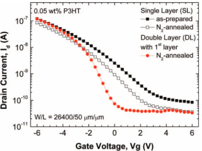
The drain current-gate voltage (Id-Vg) properties of the fabricated
PTFTs and DPTFTs are shown in Fig.2. The weight percentages of solutions of P3HT in chloroform for the PTFTs and the first layer of DPTFTs were (a) 0.05, (b) 0.1, and (c) 0.4 wt%. The thickness of the second layer of the DPTFTs was fixed by coating it with the 0.4 wt% P3HT solution. As expected, the electrical characteristics were improved for on-current level, on/off current ratio, and sub-threshold swing for single-layer PTFTs with N2 post-annealing.3,4
Characteristics of the as-prepared PTFTs are not shown, for the sake of simplicity. However, significant enhancements were observed in the proposed DPTFTs with the N2-annealed first layer. An enhancement
of greater than one order of magnitude on the on-current level, greater
Figure 2. Transfer current characteristics of PTFTs and DPTFTs that PTFT channels or the first layers of DPTFTs use (a) 0.05, (b) 0.1 and (c) 0.4 wt% P3HT solutions. PTFTs are N2-annealed, and the first P3HT layers of DPTFTs
are either with or without N2 annealing. The second layer of DPTFTs use
0.4 wt% P3HT channel without annealing.
than two orders of magnitude in the on/off current ratio, and a steeper subthreshold swing for the DPTFTs with the 0.05 wt% P3HT first layer were observed. Slightly less significant improvements were observed for those with the 0.1 wt% P3HT first layer. To exclude the possibility that the improvements resulted from the thicker active layer, char-acteristics of the DPTFTs with the as-prepared first layer were also observed. An increased on-current level, but an inferior on/off current ratio and subthreshold swing were observed. The result was expected when the active layer in the PTFTs thickened. To further understand the primary cause of the tremendous improvements observed in the DPTFTs, PTFTs with a thicker P3HT channel formed by the 0.4 wt% solution were also fabricated. The Id-Vgcharacteristics of the PTFTs
with a thicker P3HT layer are shown in Fig.2c. DPTFTs with a thicker N2-annealed first P3HT layer show a better subthreshold swing and
on/off current ratio, but no gain on the on-current level compared to the PTFTs with a N2-annealed thicker channel. This result implies
that the on-current, which is increased by using the double-coated structure, decreases with the thicker N2-annealed P3HT first layer.
The properties of DPTFTs with the as-prepared first layer (Figs.2a
and2b) were similar to those of PTFTs with a thick single-channel layer, (Fig.2c). However, the DPTFTs with the N2-annealed first layer
showed properties that were superior to those of the DPTFTs with the as-prepared first layer, or PTFTs with a thick channel. The extracted values of the saturation field effect mobility, on/off current ratio, and subthreshold swing for these samples are shown in summary form in TableI.
To gain insight on the enhanced performance induced by incor-porating a double- coated channel layer, we further investigated the characteristics of DPTFTs with different thicknesses in the second layer. We found that their properties were different from those shown in Fig. 2. Thus, we extracted the contact resistances of PTFTs by using the transmission line method (TLM). The drain current-gate voltage (Id-Vg) characteristics of the fabricated PTFTs and DPTFTs
are shown in Fig.3. The weight percentages of the solutions of P3HT in chloroform for PTFTs and the first layer of DPTFTs were 0.05 and 0.1, respectively. The thicknesses of the second layer of DPTFTs were controlled to be the same as that of the first layer. Comparing DPTFTs with PTFTs shows improvements in the on-current level, in the on/off current ratio, and the subthreshold swing in the proposed DPTFTs with the N2-annealed first layer, particularly for the DPTFTs
with the 0.05 wt% P3HT first layer. However, slightly less significant improvements were observed for those with the 0.1 wt% P3HT first
double channel layers.
layer. Characteristics of DPTFTs with the as-prepared first layer, in which both the first and second layers were coated with the 0.05 wt% P3HT solution, were similar to those of PTFTs with a thicker chan-nel layer, i.e., using the 0.1 wt% solution. These results demonstrate that the improvement in performance induced by using DPTFTs with an N2-annealed first layer is still effective when the thickness of the
second layer is reduced. Furthermore, by comparing the results of the DPTFTs with the N2-annealed first layer in Fig.3with those in
Fig.2, the correlation between the improved performance in the on-current and the thickness of the second layer can be observed. The DPTFTs with an N2-annealed first layer and thicker second layer
ex-hibit more significant on/off current ratio enhancements. However, the subthreshold swing and off-current exhibited no correlations with the thickness of the second layer. The contact resistances between PTFTs with the as-prepared or N2-annealed channel layer coated with the
0.05 wt% P3HT solution were extracted (Fig.4). For N2-annealed
PTFTs (Fig.4, right), the data point of the device with a channel length of 100μm under a gate voltage of −40 V is over the scale of the y-axis and higher than the position of the fitting line. For the sake of simplicity, this data point is not shown in the figure because we employed the same y-axis scale for both sides. The values of con-tact resistance are 5× 10⁻⁹ and 1.2× 10⁻¹⁰ for PTFTs with the as-prepared and N2-annealed channel layer, respectively. The
chan-nel resistances of as-prepared PTFTs were observed to be smaller
Figure 3. Transfer current characteristics of PTFTs and DPTFTs. PTFT chan-nels, or the first P3HT layers of DPTFTs, were coated with (a) 0.05 and (b) 0.1 wt% P3HT solutions. PTFTs and the first P3HT layers of DPTFTs are either with or without N2annealing. The second layer of DPTFTs were used
as the same as the first layer without annealing.
than those of N2-annealed PTFTs. This result can be interpreted by
the change in dopant concentration.7–10,14 The effects of annealing on the performances of P3HT TFTs in an N2environment are similar
to those observed in the annealed organic devices in an inert environ-ment, such as in glove box full of Ar, N2, or vacuum chamber. With N2
annealing, the dopant concentration in the P3HT decreases, so that the channel resistance and carrier injection barrier increase.9,10Moreover, thin active layer also contributes to reduce bulk current.15Therefore, leakage current, i.e., off-current, and poor subthreshold swing induced by the bulk current should be suppressed. Nevertheless, the on-current will decrease with bulk current suppression.15Lower on-current in-duced by thinner channel layer was also observable as shown in Figs.2and3. Less difference between on-current of the devices with as-prepared and N2-anneled, single layer channels, as shown in Fig.3,
might be due to improvement in crystallinity of P3HT. Fortunately, the on-current of DPTFTs (N2-annealed first layer and thick second layer)
is as high as that of PTFTs with thick channel layer as shown in Fig.2. However, there might be issue on the viability of double-coated channel structure. The performance enhancements might be suggested to have resulted from a specific action on the N2-annealed first layer
while coating the second layer. For example, the solvent in the solu-tion for second layer coating might have redissolved the first layer, and thus, a new single P3HT layer was formed, instead of the structure that was proposed. This hypothesis contradicts that the extent of the performance enhancement correlates with the thickness of the second layer. If there was only a residual layer, the on/off current ratio would
Figure 4. Contact resistances of PTFTs with as-prepared or N2-annealed
decrease with increased thickness of channel layer. But, in contrast, on/off current ratio was increased. Moreover, if the effect of redis-solving was critical, the properties of the devices would be related to the thickness of the first P3HT layer. In other words, the thinner N2-annealed first layer would undergo a more significant impact from
redissolution because the thin N2-annealed first layer might be fully
redissolved. Furthermore, the dopant concentration of a new single P3HT layer should not be as low as that of the N2-annealed P3HT
layer, i.e., the dopant concentration should be similar to that of the as-prepared P3HT layer. Accordingly, the characteristics of the de-vice with the new single P3HT layer, which was formed by a second coating of P3HT on a thin N2-annealed first layer, should be similar to
those of PTFTs with the as-prepared channel layer. If devices with the new single P3HT layer formed by second coating P3HT on a thick N2
-annealed first layer, the characteristics of the device should be similar to those of the PTFTs with the N2-annealed channel layer. However,
this argument conflicts with the results shown in Figs.2and3. Instead, the situation is contrary, i.e., DPTFTs with the thin N2-annealed first
layer exhibit conspicuous performance improvements. Furthermore, in some articles, the authors formed the bilayer structure by using the same solvent or solvents applicable to both layers.16–19In their works, performance difference between the devices with bilayer and bulk-heterojunction active layers could still be observed.16,17The device with the bulk-heterojunction structure was used as a comparison and formed by blending the same two materials as in the bilayer forma-tion. The results showed different device performances in their bilayer structure deposition performed with different sequences.19Thus, fab-ricating the bilayer structural active layer by using the same solvent was feasible. Furthermore, an intermixed zone between the upper and under layers was observed after formation of the bilayer structure.17 The under layer survived after spin coating the upper layer, despite the under layer not being annealed. Therefore, the re-dissolution effect is considered minor in this study, so that we could neglect it. Moreover, PTFT and DPTFT thicknesses described in the experiment can be considered evidence.
To better understand DPTFT properties with the N2-annealed first
layer, specifically for on-current and threshold voltage shift, a simpli-fied equivalent circuit is proposed and shown in Fig.5. The circuit is lumped into the cross-sectional structure of a DPTFT. For DPTFTs with the N2-annealed first P3HT layer, Rch1is larger than Rch2. Rch1
and Rspcan be varied by the gate bias. They decrease or increase
de-pending on whether the gate is biased at a negative voltage or positive voltage, respectively. Before formation of the accumulation layer, Rsp
is smaller than Rch1because the channel length is considerably larger
than the thickness of the first layer. There is a possibility that the carrier will conduct through the sidewall path and the second layer if the sum of 2Rspand Rch2is smaller than Rch1. For the results shown in
Fig.2, Rch2of the second P3HT layer coated using the 0.4 wt%
solu-tion is substantially smaller than Rch1of the N2-annealed first P3HT
Figure 5. Schematic cross section of a DPTFT incorporating the simplified equivalent circuit. The circuit includes the contact resistance between the electrodes and the semiconductor, Rc, and channel resistances of first and
second P3HT layer, Rch1and Rch2, respectively, and resistance of sidewall
path through the first layer to the second layer, Rsp.
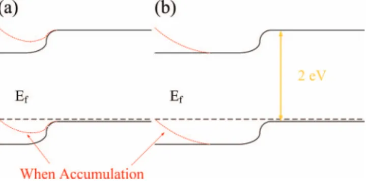
Figure 6. Band structures of DPTFTs with (a) thin and (b) thick first P3HT layers. For the sake of simplicity, we illustrate only the band structure of DPTFTs that are biased at flatband or accumulation mode.
layer, which was coated by the 0.05 or 0.1 wt% solution. Therefore, a substantially larger on-current is observed, the earlier conduction, i.e., prior to the conduction in the accumulation layer, is also found to be relative to the positive-shifted threshold voltage, as shown in Figs.2a
and2b. Additionally, if the thickness of the second layer is fixed simi-larly to the first layer, the difference between Rch2and Rch1is reduced,
although Rch2is still smaller than Rch1. Therefore, the improvement
in on/off current ratio resulted from the enlarged on-current by the presence of second layer was lowered. Moreover, when the first layer is grown, Rspand Rch1tend to increase and decrease, respectively. The
sum of Rspand Rch2might only be less small than, or equal to, Rch1,
thus leading to the results shown in Fig.3.
In addition to the simplified equivalent circuit, the illustrative band structure can be used to explain the improvements. Fig.6shows the illustrative band structures of DPTFTs with (a) thin and (b) thick N2-annealed first P3HT layers hypothesized in this study after
ap-plying external bias. The DPTFTs are biased at a flatband or accu-mulation mode. As discussed, for the results of Fig.4, the number of holes, which are induced by species in an air atmosphere in the first N2-annealed P3HT layer, should be less, compared to that in the
second P3HT layer, which was not subjected to N2 annealing
dur-ing fabrication.7,8The effect of dopant concentration in P3HT before and after N2annealing can be also correlated to the different
thresh-old voltages, which resulted in different Fermi levels.3,9The results of UV-Vis spectroscopy by Zen et al. showed that the band gaps of P3HT before and after N2annealing were almost the same.10Consequently,
a built-in potential presented because of the energy difference of the Fermi level at the interface of these two stacked layers. For DPTFTs using a sufficiently thin first layer, the entire band bending of the first layer that occurred when DPTFTs were biased at a negative gate voltage permitted barrier lowering and facilitated hole population in the second P3HT layer. These holes in the second channel are bene-ficial for transportation because they are separate from the interface between the gate oxide and P3HT layer and certainly experience less scattering, which consequently result in an improved on-current level and subthreshold swing.
Fig.7shows the Id-Vg characteristics of DPTFTs with a thinner
gate dielectric and N2-annealed first active layer accomplished by the
solution of 0.05 wt%. The second P3HT layer of DPTFTs was coated using the same solution of the first layer. The PTFTs with the as-prepared or N2-annealed channel are used as the control. The DPTFTs
using a thin gate oxide and first active layer exhibit not only tremen-dously scaled down operation voltage, but also these improvements. The subthreshold swing can be reduced to less than 1 V/decade, which is an impressive value for PTFTs. Moreover, the improvements of the on/off current ratio and subthreshold swing of DPTFTs are still ob-servable when the material of the second layer is changed. Fig.8shows the Id-Vgcharacteristics of DPTFTs with the N2-annealed first layer
coated by the 0.05 wt% solution and the F-SWCNT-blended P3HT second layer. The characteristics of PTFTs with the N2-annealed,
Figure 7. Id-Vg characteristics of DPTFTs with thinner gate dielectric and
N2-annealed first active layer. Both channel layers were coated with a solution
of 0.05 wt%. PTFTs with as-prepared or N2-annealed P3HT channel used as
the control.
channel, and DPTFTs with the N2-annealed, 0.05 wt%, first layer
and the conventional, 0.2 wt%, second layer are included in Fig.8for a comparison. After doping by F-SWCNTs, the on-current improved, and the poor on/off current ratio and subthreshold swing were ob-served to be similar to the results of our earlier study.20These might be due to the poor interface between the blended channel and gate oxide, or the increased bulk current that can act as a reference to the lower contact resistance.20In addition, compared with the PFTTs with the N2-annealed channel, the DPTFTs with the N2-annealed,
0.05 wt%, first layer and the conventional, 0.2 wt%, second layer exhibit similar improvements as those shown in Fig.2. However, the improvements can still be observed for the DPTFTs with the N2-annealed, 0.05 wt%, first layer and the F-SWCNT-blended P3HT
second layer. Compared with PTFTs with the blend channel, over 20-fold and twofold of improvements on the on/off current ratio and subthreshold swing, respectively, were obtained. The on-current de-creased, possibly because of the difference in contact resistance; that
Figure 8. Id-Vg characteristics of DPTFTs with N2-annealed, which was
coated with 0.05 wt% P3HT solution, first layer and F-SWCNTs blended P3HT second layer. The performance of PTFTs with the F-SWCNTs blended P3HT channel is included for comparison. PTFTs, the channel of which was formed by 0.05 wt% P3HT solution, and DPTFTs with an N2-annealed first
layer, the first layer and second layer of which were coated by 0.05 and 0.2 wt% P3HT solutions, respectively, were also used as the control. The drain voltage is−60 V.
higher injection barrier between Au and P3HT and also greater film resistance than the as-prepared P3HT layer because of the reduced dopant concentration. Both result in the reduced bulk current that benefits the subthreshold current and off-current as the DPTFTs are turned off; and ii) The equivalent circuit and illustrative band structure of DPTFTs show that the carriers could conduct in the second layer as the devices are biased at the mode before formation of the accu-mulation layer, thus leading to the positive-shifted threshold voltage and the dependence of performance upon the thickness of the second layer.
Both the improvements in subthreshold performances and on-current due to the reduced bulk on-current and high conductivity of second layer can be obtained by using double-coated channel layer structure. Furthermore, this study also demonstrated that improvements induced by the double-coated channel layer can still be observed as the thin gate oxide and the F-SWCNT-blended P3HT second layer were used for the DPTFTs.
References
1. H. Sirringhaus, P. J. Brown, R. H. Friend, M. M. Nielsen, K. Bechgaard, B. M. W. Langeveld-Voss, A. J. H. Spiering, R. A. J. Janssen, E. W. Meijer, P. Herwig, and D. M. de Leeuw,Nature, 401, 685 (1999).
2. H. Sirringhaus, N. Tessler, and R. H. Friend,Science, 280, 1741 (1998). 3. G. Wang, J. Swensen, D. Moses, and A. J. Heeger,J. Appl. Phys., 93, 6137 (2003). 4. S. Cho, K. Lee, J. Yuen, G. Wang, D. Moses, A. J. Heeger, M. Surin, and R. Lazzaroni,
J. Appl. Phys., 100, 114503 (2006).
5. H. Yang, T. J. Shin, Z. Bao, and C. Y. Ryu,J. Polym. Sci. Part B: Polym. Phys., 45, 1303 (2007).
6. Y. D. Park, H. S. Lee, Y. J. Choi, D. Kwak, J. H. Cho, S. Lee, and K. Cho,Adv. Funct. Mater., 19, 1200 (2009).
7. M. S. A. Abdou, F. P. Orfino, Z. W. Xie, M. J. Deen, and S. Holdcroft,Adv. Mater., 6, 838 (1994).
8. S. Hoshino, M. Yoshida, S. Uemura, T. Kodzasa, N. Takada, T. Kamata, and K. Yase, J. Appl. Phys., 95, 5088 (2004).
9. B. H. Hamadani, H. Ding, Y. Gao, and D. Natelson,Phys. Rev. B, 72, 235302 (2005). 10. A. Zen, J. Pflaum, S. Hirschmann, W. Zhuang, F. Jaiser, U. Asawapirom, J. P. Rabe,
U. Scherf, and D. Neher,Adv. Funct. Mater., 14, 757 (2004).
11. M. J. Deen, M. H. Kazemeini, Y. M. Haddara, J. Yu, G. Vamvounis, S. Holdcroft, and W. Woods,IEEE Trans. Electron Devices, 51, 1892 (2004).
12. E. von Hauff, F. Johnen, A. V. Tunc, L. Govor, and J. Parisi,J. Appl. Phys., 108, 063709 (2010).
13. L. Res´endiz, M. Estrada, A. Cerdeira, B. I˜niguez, and M. J. Deen,Org. Electron., 11, 1920 (2010).
14. C. H. Chang, M. F. Chen, and C. H. Chien,J. Electrochem. Soc., 158, H854 (2011). 15. C.-H. Chang and C.-H. Chien,Org. Electron., 13, 2620 (2012).
16. R. A. Marsh, C. R. McNeill, A. Abrusci, A. R. Campbell, and R. H. Friend,Nano Lett., 8, 1393 (2008).
17. D. H. Wang, H. K. Lee, D. G. Choi, J. H. Park, and O O. Park,Appl. Phys. Lett., 95, 043505 (2009).
18. E. Kymakis, E. Koudoumas, and I. Franghiadakis,Sol. Energy Mater. Sol. Cell, 90, 1705 (2006).
19. K. Kaneto, M. Yano, M. Shibao, T. Morita, and W. Takashima,Jpn. J. Appl. Phys., 46, 1736 (2007).