vapor deposition fluorine-doped silicon dioxide
Y. L. Cheng, Y. L. Wang, H. W. Chen, J. L. Lan, C. P. Liu, S. A. Wu, Y. L. Wu, K. Y. Lo, and M. S. Feng
Citation: Journal of Vacuum Science & Technology A 22, 494 (2004); doi: 10.1116/1.1690779
View online: http://dx.doi.org/10.1116/1.1690779
View Table of Contents: http://scitation.aip.org/content/avs/journal/jvsta/22/3?ver=pdfcov
Published by the AVS: Science & Technology of Materials, Interfaces, and Processing
Articles you may be interested in
Methods of producing plasma enhanced chemical vapor deposition silicon nitride thin films with high compressive and tensile stress
J. Vac. Sci. Technol. A 26, 517 (2008); 10.1116/1.2906259
Effects of thermal annealing on the structural, mechanical, and tribological properties of hard fluorinated carbon films deposited by plasma enhanced chemical vapor deposition
J. Vac. Sci. Technol. A 22, 2321 (2004); 10.1116/1.1795833
Effect of fluorine incorporation on silicon dioxide prepared by high density plasma chemical vapor deposition with SiH 4 O 2 NF 3 chemistry
J. Appl. Phys. 96, 1435 (2004); 10.1063/1.1767979
Thermal stability enhancement of Cu/WN/SiOF/Si multilayers by post-plasma treatment of fluorine-doped silicon dioxide
J. Appl. Phys. 85, 473 (1999); 10.1063/1.369410
Structure of fluorine-doped silicon oxide films deposited by plasma-enhanced chemical vapor deposition
plasma chemical vapor deposition fluorine-doped silicon dioxide
Y. L. ChengDepartment of Material Science and Engineering, National Chiao-Tung University, Hsin-Chu, Taiwan, Republic of China
Y. L. Wang,a)H. W. Chen, and J. L. Lan
Taiwan Semiconductor Manufacturing Company, Ltd., Hsinchu, Taiwan, Republic of China
C. P. Liu
Department of Material Science Engineering, National Cheng-Kung University, Tanani, Taiwan, Republic of China
S. A. Wu
Taiwan Semiconductor Manufacturing Company, Ltd., Hsinchu, Taiwan, Republic of China
Y. L. Wu
Department of Electrical Engineering, National Chi-Nan University, Nan-Tou, Taiwan, Republic of China
K. Y. Lo
Department of Applied Physics, National Chiayi-University, Chiayi, Taiwan, Republic of China
M. S. Feng
Department of Material Science and Engineering, National Chiao-Tung University, Hsin-Chu, Taiwan, Republic of China
共Received 26 June 2003; accepted 2 February 2004; published 14 April 2004兲
Thermal stability of fluorine-doped silicon dioxide films deposited by high-density plasma chemical vapor deposition as a function of deposition temperature were investigated in this study. Both thermal desorption spectrum and annealing test results show that SiOF films deposited above 400 °C have better thermal stability. Furnace annealing data indicate that nonuSiuFu bonding fluorine does exist in low-deposition-temperature SiOF films. Furthermore, secondary-ion mass spectrometer results also reveal that the fluorine in SiOF films with a lower-deposition temperature is easily diffused out and turned into the underlayer, which results in less thermally stable SiOF films. Moreover, short-loop simulation results have been subsequently tested and it was concluded that the deposition temperature of the SiOF film is extremely important for thermal stability. © 2004 American Vacuum Society. 关DOI: 10.1116/1.1690779兴
I. INTRODUCTION
With recent progress of high integration and modern ultralarge-scale integration achieving gate widths of less than 0.25m, it has become necessary to further improve device operating speed, which is limited by the capacitance of inter-metal dielectric 共IMD兲 capacitance. To reduce the IMD ca-pacitance, fluorine-doped silicon dioxide 共SiOF兲1 films de-posited by high-density plasma chemical vapor deposition
共HDP-CVD兲 have been introduced in an advanced IMD
ap-plication. The HDP-CVD technique has been demonstrated to have good gap-filling capability and film stability.2,3 Moreover, in 1998, Yang et al.4produced SiOF films in 0.18 m logic devices. As a consequence, SiOF films are consid-ered a suitable and a manufacturable low dielectric constant
共low-k兲 IMD for devices below 0.25m.
Many researchers have studied the formation process of SiOF films, viewing it as having a low k, excellent gap-filling ability due to in situ etching by SiF4, and being void
free. They point out that the higher fluorine concentration
would lower the dielectric constant5– 8and improve the gap-filling ability. However, these researchers also express cau-tion that SiOF films have a thermal stability issue that affects the integration. The subsequent deposition of a SiOF-capped silicon-dioxide (SiO2), metal film, and passivation layer has
shown blistering after the alloying process.9As a result, pre-cursors, reaction methods, and optimized process conditions have been proposed to improve the thermal stability of SiOF films.10–13
In this work, we conducted a comprehensive study of the dependence on the deposition temperature of the physical properties and thermal stability of SiOF films prepared by HDP-CVD using Ar, O2, SiH4, and SiF4 gas. The relevance
of the deposition temperature in influencing the properties of SiOF films is reported. Also, a comparative analysis of ther-mal desorption spectrum 共TDS兲, annealing test, and secondary-ion mass spectrometer共SIMS兲 results allow us to determine the thermal stability of individual SiOF films with varying deposition temperature.
a兲Also at: Department of Electrical Engineering, National Chi-Nan Univer-sity, Nan-Tou, Taiwan, Republic of China.
II. EXPERIMENT
The SiOF films were prepared in an Ultima HDP-CVD
Applied Materials Centura 5200 system using
Ar/O2/SiH4/SiF4 as reaction gas. The gas flow rate of Ar, O2, SiH4, and SiF4 were 50, 110, 45, and 30 cm3/min, re-spectively. The deposition temperature was detected at the back side of the deposited wafer by a wafer temperature monitor. The back side He pressure was adjusted to control the deposition temperature, which we varied from 350 to 450 °C. The as-deposited films were analyzed for thickness and refractive index共RI, at 633 nm兲 by reflectometry and/or ellipsometry using the Nano-Spec 9100. This thickness of the SiO film is the net-deposition 共ND兲 thickness under rf bias conditions, which is the sum of deposition, sputter, and etch. The sputter 共S兲 rate was measured by sputtering the SiOF films for 60 s on a blanket wafer using Ar gas. The pure deposition 共PD兲 thickness 共no sputter/no etch effects兲 was determined by setting the bias rf to zero on a blanket wafer. Therefore, the removal thickness due to sputter and etch (S⫹E) effects should be the PD thickness minus the ND thickness. The etch共E兲 rate was then calculated by sub-tracting the thickness of S from the removal thickness of sputter and etch (S⫹E). TDS and furnace alloy samples were deposited directly on bare silicon wafers. In addition, SIMS was used to analyze the film structure based on a sili-con wafer that was first covered with a SiO2 film, then a
SiOF film of different temperatures, and then capped with a SiO2 layer.
The furnace annealing condition reached 425 °C for 60 min in nitrogen ambients and the alloying process required seven heating/cooling cycles in total. Next, the fluorine con-centration was measured before and after alloying by infra-red 共IR兲 spectroscopy using a Bio-rad Fourier transform in-strument, using the SiuF band at about 930 cm⫺1and also using x-ray fluorescence 共XRF兲. We quantified the Si–F/ Si–O peak–height ratios in the reflectance mode. The IR analysis was performed at a resolution of 4 cm⫺1, averaging 16 scans. XRF detected F bonded in both SiuF and non
uSiuFu configurations in 200 second scans. The SiOF
films with different deposition temperatures were prepared, and then the gap-filling capability of the various SiOF films was determined by scanning electron microscopy 共SEM兲. Subsequently, the structure of short-loop samples was simu-lated on a 0.18m IMD scheme, to verify and support pre-vious TDS and alloying results.
III. RESULTS AND DISCUSSIONS A. Film property
Figure 1 shows the refractive index of SiOF thin films,
measured by ellipometry, as a function of the SiOF deposi-tion temperature. For these films deposited by HDP-CVD, the refractive indices are 1.40–1.45, which are lower than the 1.46 value of thermal oxide SiO2. It is well known that
the refraction index is closely related to the porosity of these SiO2-based materials, being smaller for higher porosity.
Therefore, porosity might be one reason for the lower refrac-tive indices. However, as shown in Fig. 1, the RI decreases appreciably with decreasing SiOF film deposition tempera-ture, but with increasing fluorine content. This shows that the lower RI may also be influenced by fluorine incorporation into SiO2. Further support for this may be found with the IR spectra. We find that at lower deposition temperature, the peak of the SiuO stretching band shifts to a higher fre-quency, in the presence of a high concentration of fluorine in the structure. As a consequence, the SiuOuSi bond angle opens up slightly, resulting in a cage structure 共porosity兲 in the film. This structure causes the density of the film to de-crease. Therefore, the RI also decreases with decreasing deposition temperature. Agreeing with this result, the dielec-tric constant of the as-deposited SiOF film decreases to 3.346 at 350 °C from 3.964 at 450 °C. The reduction of electronic polarization by more SiuF bonds and by an increment in porosity in the SiOF film, both contribute to a lower k. Table I summarizes the trends for increasing deposition tempera-tures. The deposition rate increases as the SiOF deposition temperature decreases owing to fluorine having less thermal energy in which to provide plasma etching. For higher-deposition temperatures, the SiOF film becomes denser as a result of the plasma etching ability to remove weak bonds, and results in a material having lower wet etch rates. It is worth noticing that the hardness of the SiOF films decreases as the deposition temperature decreases due to an increase in porosity and decrease in cross linking due to reactor
incor-FIG. 1. Effect of deposition temperature on the concentration of fluorine and
refractive index for SiOF film. TABLEI. Property of SiOF film trends at 350– 450 °C-deposition temperature.
poration of terminal SiuF bonds. The hardness of the low-k film is an essential property during processing with chemical mechanical polishing共CMP兲.
B. Gap-filling ability
As the minimum geometry of integrated-circuit devices becomes increasingly smaller, the separation between metal lines becomes smaller, as well. Because the deposition rate is lower at the side wall of the metal gaps than at the bottom of the gap, HDP-CVD has been introduced to enhance the gap-filling ability owing to the sputter ability of high-density plasma. However, it still has difficulties in filling higher-aspect ratio gaps, without voids 关Fig. 2共a兲兴. On the other hand, we can use the etching ability of fluorine to facilitate the deposition to fill the smaller gap关Fig. 2共b兲兴. Therefore, to investigate the effect of deposition temperature on the gap-filling ability, we separated the HDP-CVD SiOF deposition process into three main reactions: Deposition (D), sputter (S), and etch 共E兲. Furthermore, we also defined the param-eter D/(S⫹E) as the filling index. The better the gap-filling capability, the smaller the D/(S⫹E) value. The cal-culated results are summarized in Table II. As seen in Table II, the E/(S⫹E) value quantifies the contribution of the etch
component of the total removal in the HDP-CVD SiOF pro-cess, and this value increases with the rise of deposition perature. The result also shows that the sputter rate is tem-perature independent in our experimental temtem-perature range. Thus, the etch rate contribution to the total removal rate in-creases with temperature. There is about a 5% increase in etch rate with an increase of 100 °C temperature, which causes a decrease of the D/(S⫹E) ratio. Therefore, we infer that SiOF films with a higher deposition temperature pre-pared by HDP-CVD should have a high gap-filling capacity compared to those with a lower deposition temperature.
The gap-filling ability was investigated by depositing SiOF films with different deposition temperatures wafers pattered with different metal widths/gaps. Figure 3 reveals that a 350 °C-deposited SiOF film can fill into the metal gap with 0.25 m spacing, but not reach the void-free require-ment for a 0.21 m gap 关Fig. 3共a兲兴. On the other hand, a higher deposition temperature 共⬃450 °C兲 can fill a 0.21m metal gap 共aspect ratio was 3.6兲 with no metal clipping, which implies that the etch ability of the F atom has in-creased abruptly at the higher temperature on the wafer. Again, we also demonstrate that the deposition rate decreases with increased deposition temperature due to the fact that F etches SiO2 more effectively at high temperature.
C. Thermal stability-outgassing issues
In real interconnect fabrication, thermal treatment is an indispensable step. Here, the interconnect medium consists of up to eight separate layers, all of which are deposited at FIG. 2. Concept of HDP-CVD gap filling:共a兲 HDP-CVD and 共b兲 F-doped
HDP-CVD.
FIG. 3. SEM image of SiOF film for checking gap filling (height/gap
⫽0.6m/0.21m):共Left-hand side兲 350 °C, 共right-hand side兲 450 °C.
TABLEII. Effect of deposition temperature on gap-filling parameters of SiOF process. Deposition
temperature
共°C兲 Deposition rateD共Å/min兲
Sputter rate S共Å/min兲
Etch rate
E共Å/min兲 E/(S⫹E) E/S D/(S⫹E) D/S D/E E/S
350 3607 1541 1011 0.396 0.656 1.374 2.341 3.568 0.656
375 3553 1548 1028 0.399 0.656 1.340 2.295 3.456 0.664
400 3506 1553 1067 0.407 0.687 1.300 2.258 3.286 0.687
425 3480 1538 1080 0.412 0.702 1.291 2.263 3.223 0.702
about 400 °C. As a result, a suitable interconnect dielectric should possess excellent thermal resistance. To study the thermal stability of SiOF films with varying deposition tem-perature, the films were annealed in N2 ambient for 1 h at 425 °C. The film thickness, RI, and fluorine concentration
共IR value兲 after annealing all remained stable even after
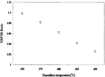
re-peated annealing tests共seven times兲 through the entire range of deposition temperatures. This points out that the SiuO and SiuF bonds in SiOF films have enough thermal resis-tance against a 425 °C heat treatment. However, the fluorine content measured by XRF gradually declined and reached saturation after the third annealing test. Moreover, the mag-nitude of this decline is dependent upon the deposition tem-perature of SiOF films. The SiOF film with a lower-deposition temperature has a larger change in XRF value, as shown in Fig. 4. IR was used to monitor the SiuF/SiuO ratio, calibrated with Rutherford backscattering, and XRF detected total fluorine content共including bonding SiuF and nonuSiuFu bonding fluorine兲. Consequently, we can use Eq. 共1兲 to calculate the amount of nonuSiuFu bonding:
XRF/IR⫽1⫹共nonuSiuFu兲/SiuF. 共1兲
The higher XRF/IR ratio means a higher amount of non
uSiuFu bonding fluorine. As shown in Fig. 5, the lower
deposition temperature of the SiOF process has more non
uSiuFu bonding fluorine. This can explain the result of
Fig. 4. As the SiOF film with a lower-deposition temperature was immersed into a N2ambient at an elevated temperature,
more nonuSiuFu bonding fluorine outgassed in the ther-mal process. Furthermore, after three cycles of the annealing process, for the SiOF film with a deposition temperature above 400 °C, the outgassing reached saturation. On the con-trary, the fluorine at. % 共XRF value兲 kept decreasing for SiOF films with deposition temperatures below 400 °C, even after seven cycles of the annealing process. This implies that SiOF films deposited at temperatures lower than 400 °C have greater amounts of either weak SiuF bonding or nonbonded fluorine 共free fluorine兲. Hence, the weaker SiuF units will be broken, or free fluorine will be outgassed by the thermal process. Considering this outgas as excess fluorine, this ex-cess could possibly be avoided by the use of a lower gas
ratio (SiF4/SiH4) and, thereby, keep the fluorine
concentra-tion stable after heat treatment. It is speculated that more SiF4 共less SiH4) would create a greater F% concentration
without being bonded with the Si atom. Of course, lowering the gas ratio might also impact the k-lowering property of fluorine. So, a proper balance must be struck. A comprehen-sive study will be reported in another paper.
The thermal stability of SiOF films is also studied using TDS. Gas desorption from films, especially at a lower tem-perature, has been a concern for device reliability issues, such as the failure of pressure cooling, thermal cycle, and thermal stress tests. The TDS spectra with respect to the mass fragment 18M /e, 19M /e, and 20M /e for SiOF films with different deposition temperatures are checked 共not shown兲. Corresponding to these masses, H2O, F, and HF desorption from SiOF films at a lower temperature for a lower deposition temperature are summarized in Table III. As shown, the desorption temperature of Ar is relatively insen-sitive to the SiOF film deposition temperature. On the other hand, the desorption temperatures of H2O, F, and HF are
strongly dependent upon the deposition temperature. Higher-deposition-temperature SiOF films have a higher desorption temperature and a lower-desorption pressure. A higher onset of the evolution of desorption temperature means that the film has greater thermal stability during postthermal pro-FIG. 4. Difference of XRF of SiOF films with varying deposition
tempera-ture.
FIG. 5. XRF/Fourier transform IR ratio of SiOF films with varying deposi-tion temperature.
TABLEIII. TDS analysis for SiOF films with varying deposition tempera-tures.
Deposition temperature
350 400 425 450
共°C兲
Ar onset of evolution共°C兲 450 455 445 467
Ar peak pressure (10⫺7Torr) 0.1 0.1 0.1 0.1
H2O onset of evolution共°C兲 452 467 467 520
H2O peak pressure (10⫺7Torr) 1.0 1.0 1.0 0.5
F onset of evolution共°C兲 435 450 467 490
F peak pressure (10⫺7Torr) 1.0 1.0 1.0 0.5
HF onset of evolution共°C兲 410 420 450 467
HF peak pressure (10⫺7Torr) 1.0 1.0 1.0 0.5
cesses. Consequently, we have demonstrated that SiOF films with a higher-deposition temperature have less moisture con-tent, greater thermal stability, and better suitability for the IMD application in the back-end process.
D. Fluorine stability-diffusion issues
Fluorine stability with respect to diffusion within SiOF films strongly influences its utility in IMD integration, with Al wiring delamination as one important area of concern. Fluorine stability was investigated by SIMS using a sand-wich structure, consisting of oxide/SiOF/oxide, where the oxides are 2000 Å of SiO2. This sandwich structure was
deposited on the Si substrate. All samples were annealed at 425 °C for 1 h in a N2 atmosphere. The annealing test was
performed seven times.
As observed in Fig. 6共a兲, when the SiOF film underwent one thermal treatment, the fluorine atoms diffused into the adjacent oxide films. However, this diffusion was rather modest and the fluorine profile remained quite sharp at the SiOF/SiO2 interface. Therefore, we concluded that the
driv-ing force of fluorine diffusion is the overall thermal budget. Figure 6共b兲 compares the effect of deposition temperature for fluorine diffusion stability. It shows that the SiOF film with a lower-deposition temperature共350 °C兲 exhibits a higher fluo-rine diffusion capability. This is the same data shown in Fig.
6共a兲. The fluorine diffusion length for the SiOF film at 350 °C deposition temperature is about⬃500 Å, higher than that 共⬃200 Å兲 of the SiOF film at 450 °C deposition tem-perature. Most of the diffused F is believed to originate as weak bonding SiuF or from free fluorine. As a conse-quence, a lower deposition temperature of the SiOF film causes weaker SiuF bonds to break and diffuse, along with the free fluorine, affecting the stability of the film.
E. Interconnect pattern wafer test
The thermal stability of SiOF films with varying deposi-tion temperature is also confirmed using actual Al intercon-nect test structures. The effect of the deposition temperature on via resistance for the design rule 共0.23 width/0.21 m spacing兲 of 0.18m using SiOF films as an IMD was also checked. Via resistance has no significant difference in any deposition temperature, ranging from 350 to 450 °C 共not shown兲. This implies that SiOF films with a deposition tem-perature from 350 to 450 °C can be well integrated with a photo and etch process. On the other hand, reliability and defects were frequently detected on patterned wafers, espe-cially in the case of lower-deposition temperatures 共350 to 400 °C兲. A serious bubble defect was observed after complet-ing a seven-layer metal structure. This type of defect was found on the metal pads, shown in Fig. 7共a兲, similar to the result of Kawashima et al.14 These defects arise from the diffusion of unstable fluorine and the reactions with the un-FIG. 7. Integration problems of SiOF film with 350 °C deposition tempera-ture:共a兲 Optical microscope image of bubble defect on Al pad and 共b兲 SEM image of film peeling.
FIG. 6. SIMS profile of SiOF film: 共a兲 Annealing effect 共deposition temperature⫽350 °C) and 共b兲 deposition temperature effect.
derlayer barrier layer共TiN兲, metal lines 共Al兲, and passivation layer (Si3N4). Another defect type, i.e., peeling, is also ob-served for a 350 °C SiOF film, as shown in Fig. 7共b兲. Peeling is hardly ever found in higher-deposition-temperature SiOF films. Additionally, it always occurred after the CMP pro-cess. A lower hardness of the SiOF film with a lower-deposition temperature was suspected because the high downforce of the CMP process. To solve these problems of a lower-temperature SiOF film, one should increase the liner and capped layer thicknesses and reduce the downforce in the CMP process. However, a sacrifice of the effective di-electric constant and CMP planarization properties may oc-cur.
IV. CONCLUSIONS
The thermal stability for SiOF deposited by HDS-CVD is highly influenced by deposition temperature. All analyses, including SIMS, TDS, and annealing thermal tests, have shown that SiOF films deposited above 400 °C have better thermal stability. However, the high deposition temperature
共over 450 °C兲 creates metal 共AlCu兲 extrusion and melting
issues. Patterned wafers with short-loop results have also demonstrated that low-deposition temperature results in F-bubble formation because of greater amount of free fluo-rine. The results of this study demonstrate that the deposition temperature of SiOF films is extremely important for the thermal stability of the film.
ACKNOWLEDGMENTS
Technical support from the Failure Analysis Laboratory of
the Taiwan Semiconductor Manufacturing Company
共TSMC兲 is acknowledged. Special thanks are also due to
Andy Chen and M. H. Yoo of TSMC for their full support.
1J. Pellerin, R. Fox, and H. M. Ho, Mater. Res. Soc. Symp. Proc. 476, 113
共1997兲.
2J. A. Theil, F. Mertz, M. Yairi, K. Seaward, G. Ray, and G. Kooi, Mater.
Res. Soc. Symp. Proc. 476, 31共1997兲.
3H. Yang and G. Lucovsky, Mater. Res. Soc. Symp. Proc. 476, 273共1997兲. 4L. Baual, G. Passemard, Y. Gobil, H. M’saad, A. Corte, F. Pires, P. Fugier,
P. Noel, P. Rabinzohn, and I. Beinglass, Microelectron. Eng. 37, 261
共1997兲.
5
P. W. Lee, S. Mizuno, A. Verma, H. Tran, and B. Nguyen, J. Electrochem. Soc. 143, 2015共1996兲.
6W. Chang, S. M. Jang, C. H. Yu, S. C. Sun, and M. S. Liang, IEEE (1999)
IITC 99-131.
7
H. J. Shin, S. J. Kim, B. J. Kim, H. K. Kang, and M. Y. Lee, IEEE (1998) IITC98-211.
8H. M. Baad, Proceedings of 1999 DUMIC Conference.
9T. Tamura, J. Saki, Y. Inoue, M. Satoh, and H. Youshitaka, Jpn. J. Appl.
Phys., Part 1 37, 2411共1988兲.
10
C. F. Yeh, Y. C. Lee, K. H. Wu, Y. C. Su, and S. C. Lee, J. Electrochem. Soc. 147, 330共2000兲.
11S. Agraharam, D. W. Hess, P. A. Kohl, and S. B. Allen, J. Electrochem.
Soc. 147, 2665共2000兲.
12
S. Lee and J. W. Park, J. Vac. Sci. Technol. A 17, 458共1999兲.
13T. Homma, Thin Solid Films 278, 28共1996兲.
14Y. Kawashima, T. Ichikawa, N. Nakamura, S. Obata, Y. Den, H. Kawano,
T. Ide, and M. Kudo, IEEE Trans. Semicond. Manuf. 12, 302共1999兲.