國 立 交 通 大 學
電子工程學系 電子研究所碩士班
碩 士 論 文
高壓製程靜電放電防護元件設計與其安全操作
範圍之研究
Study of Electrostatic Discharge Protection
Devices and Their Safe Operating Area in
High-Voltage BCD SOI Process
研 究 生: 黃筱晴 (Hsiao-Ching Huang)
指導教授: 柯明道教授 (Prof. Ming-Dou Ker)
高壓製程靜電放電防護元件設計與其安全操作
範圍之研究
Study of Electrostatic Discharge Protection
Devices and Their Safe Operating Area in
High-Voltage BCD SOI Process
研 究 生:黃筱晴
Student: Hsiao-Ching Huang
指導教授:柯明道教授
Advisor: Prof. Ming-Dou Ker
國立交通大學
電子工程學系 電子研究所
碩士論文
A Thesis
Submitted to Department of Electronics Engineering and Institute of
Electronics College of Electrical and Computer Engineering
National Chiao-Tung University
in Partial Fulfillment of the Requirements
for the Degree of
Master
in
Electronics Engineering
July 2011
Hsin-Chu, Taiwan
中華民國一百年七月
高壓製程靜電放電防護元件設計與其安全操作
範圍之研究
學生:黃筱晴
指導教授:柯明道教授
國立交通大學 電子工程學系電子研究所碩士班
ABSTRACT (CHINESE)
在智慧型高功率科技中,高壓電晶體已經廣泛運用於顯示器積體電路、電源 供應、電源管理,和汽車電子等應用上。然而,隨著製程複雜度的提升以及工作 環境日益惡化,高壓積體電路的各種可靠度議題逐漸受到重視,其重要性不容小 覷。在許多可靠度的規範守則當中,靜電放電防護 (ESD) 以及安全操作範圍 (SOA) 已成為不可或缺的可靠度議題。為了減少晶片總面積,希冀設計出同時 擁有穩健之靜電放電防護能力以及廣大之安全操作範圍的高壓電晶體。因此,本 論文旨在探討高壓電晶體之靜電放電防護以及安全操作範圍議題。 本篇論文提出以圓形以及橢圓形之佈局方式呈現橫向擴散金屬氧化物半導體 (LDMOS) ,並實現於 0.5-m 100-V bipolar CMOS DMOS (BCD) silicon on
insulator (SOI) 製程。在許多高壓應用當中,高壓電晶體本身具備抵擋靜電放電 之能力是較受歡迎的。因此本文提出於橫向擴散金屬氧化物半導體嵌入矽控整流 器 (silicon controlled rectifier, SCR) 以提高靜電放電防護能力。實驗數據顯示, 嵌入矽控整流器確實可有效提升靜電放電防護能力。然而,嵌入矽控整流器的相 對位置安排對靜電放電防護能力有不可忽視的影響。此外,本文也探討各種佈局 參數對於靜電放電防護能力的影響。
護能力,但其電性安全操作範圍 (electrical SOA) 嚴重縮小,而且承受未箝制電 感性切換 (unclamped inductive switch, UIS) 的能力也大幅降低。此外,本文探討 未箝制電感性切換的特性,並發現若橫向擴散金屬氧化物半導體之啟動電流越大, 其承受未箝制電感性切換的能力就越好,因此,在未來的未箝制電感性切換之研 究中,可朝著研究其啟動電流方向努力
Study of Electrostatic Discharge Protection
Devices and Their Safe Operating Area in
High-Voltage BCD SOI Process
Student: Hsiao-Ching Huang
Advisor: Prof. Ming-Dou Ker
Department of Electronics Engineering &Institute of Electronics
College of Electrical and Computer Engineering
National Chiao-Tung University
ABSTRACT (ENGLISH)
High-voltage (HV) transistors in smart power technologies have been extensively used for display driver integrated circuits (ICs), power supplies, power management and automotive electronics. The importance of reliability issue should not be underestimated in HV ICs as a result of the process complexity and stringent operating environments. Among the various reliability specifications, electrostatic discharge (ESD) protection and safe operating area (SOA) are becoming the essential issues for HV ICs. A HV transistor simultaneously exhibiting excellent ESD robustness and wide SOA is preferable to minimize the total chip area; hence, the aim of the thesis is to investigate the ESD performance and SOA of HV transistors.
In this thesis, lateral double-diffused metal oxide semiconductor (LDMOS) with circular and elliptic layout shapes are fabricated in a 0.5-m 100-V bipolar CMOS DMOS (BCD) silicon on insulator (SOI) process. The self-protected HV transistor
against ESD stress is popular in HV applications. The insertion of silicon controlled rectifier (SCR) to LDMOS is proposed to improve the ESD robustness. Experimental results show that it can effectively improve the ESD robustness. However, the arrangement of placing embedded SCR significantly affects the ability to withstand the ESD stress. In addition, the influence of various layout parameters on ESD robustness is studied in the thesis.
Though LDMOS with embedded SCR exhibits excellent ESD robustness, it suffers from a severe degradation of electrical SOA and a poor ability to withstand the unclamped inductive switch (UIS) stress. Besides, the characteristic of UIS is studied and it is discovered that a LDMOS has better ability to withstand the UIS stress when it has a higher trigger current. Engineering the trigger current of LDMOS accordingly can be a direction of future UIS studies.
ACKNOWLEDGEMENTS
致謝
在這兩年的碩士生涯當中,首先要感謝的是我的指導教授 柯明道老師。謝 謝您一路上的諄諄教誨以及辛勤督導,老師不僅教導我許多專業知識還有做事的 態度,讓我在這兩年中得到許多的成長,此外還要謝謝您不辭辛苦地四處奔波爭 取研究資源,讓我們的研究更加順遂,老師,謝謝您! 我要特別感謝某業界公司給予我們研究群下線機會,讓我們可以落實元件設 計並得到很好的驗證。此外還要感謝「世界先進股份有限公司」的元件工程處協 助本論文之靜電放電能力測試作業,感謝「閎康科技股份有限公司」協助本論文 之元件失效分析作業,感謝您們各方面的協助。 接下來要感謝的是陳穩義學長,謝謝學長耐心地教導我許多知識,並在很短 的時間內帶我進入高壓殿堂,在學長身上我看到對研究的堅持以及負責任的肩膀, 即使現在的我還不及學長的千分之一,但我仍然會努力向學長看齊。在此,請接 受我深深的一鞠躬,學長,謝謝您! 我還要感謝許多學長姐:分享學術論文的正哥、聰明絕頂的群祐學長、高壓 一哥暢資學長、量測達人介堯學長、超級健談的曄仁學長、包山包海的柏硯學長、 幽默風趣的立煒學長、實驗室開心果帥氣小州哥、認真負責的致廷學長、好學的 惠雯學姐、活潑開朗的倍如學姐、漂亮媽咪怡歆學姐、高壓研究很強大的哲綸學 長、熱情開朗的佑達學長、大酒窩愛唱老歌的思翰學長、豪邁的堂龍學長以及 307 所有學長姐,感謝大家一路上的照顧,謝謝您們! 還有一路陪伴我的同學們:優秀的宛彥,謝謝妳一年半的陪伴與鼓勵。做事 很有效率的易儒,謝謝你幫忙我解決研究上的問題並在危急時刻伸出援手,謝謝 你!聰明認真的豔婷、簡仲、Adley,謝謝你(妳)們兩年的陪伴以及聆聽。可愛的 學弟妹們:小中分林小孟、皮膚超級白皙的雅君、翔宇以及瑀晴,交大生活有了 你(妳)們變得有趣許多,在此祝福你(妳)們研究順遂。 最後,在此我要特別感謝我的父母親 黃聰榮先生與 石明月女士。您們對我 在生活上以及經濟上的支持,是讓我無後故之憂唸完碩士班的最大支柱。對父母 該感謝的太多,不是三言兩語可用字寫盡,在這裡誠心地對我偉大的父母親致上 最崇高的感謝。謝謝親愛的姐姐、哥哥、姐夫與可愛的姪女們給予我滿滿的愛。 還有我的男朋友 王景弘先生,感謝你這一路的付出與陪伴。 其他該感謝的人還有很多,對一路上曾經幫助過我的各位,在此一併獻上感 激之情。 黃 筱 晴 謹誌於竹塹交大 民國一百年七月CONTENTS
ABSTRACT (CHINESE) ... i
ABSTRACT (ENGLISH) ...iii
ACKNOWLEDGEMENTS ... v
CONTENTS ... vi
TABLE CAPTIONS ...viii
FIGURE CAPTIONS ... ix
Chapter 1 ... 1
Introduction ... 1
1.1 Motivation ... 1
1.2 Investigation on the Impact of Junction Curvature Effect on HV ICs ... 2
1.3 Thesis Organization ... 8
Chapter 2 ... 9
Proposed Device Structure Designs of LDMOS ... 9
2.1 The Standard Device Structure of LDMOS ... 9
2.2 The Device Structure of LDMOS with embedded SCR ... 14
2.3 IDS-VDS Characteristics ... 16
2.4 Avalanche Breakdown Voltage ... 22
Chapter 3 ... 25
Introduction to Electrostatic Discharge and Experimental Results ... 25
3.1 Introduction to Electrostatic Discharge (ESD) ... 25
3.1.1 Human Body Model (HBM) ... 25
3.1.2 Machine Model (MM) ... 27
3.1.3 Charged Device Model (CDM)... 28
3.1.4 Transmission Line Pulse (TLP) System ... 30
3.2 ESD Test Methods ... 32
3.2.1 ESD Test on I/O Pins ... 32
3.2.2 Pin to Pin ESD Test ... 34
3.2.3 VDD-to-VSS ESD Test ... 35
3.2.3 CDM ESD Test ... 36
3.3 Experimental results ... 37
3.3.1 ESD Robustness ... 37
3.3.2 Failure Analysis ... 42
3.3.3 The influence of layout parameters on ESD robustness ... 47
Chapter 4 ... 56
Investigation on Safe Operating Area (SOA) and Experimental Results ... 56
4.1 Introduction to SOA ... 56
4.1.1 Classification of SOA ... 56
4.1.2 Characteristic of Unclamped Inductive Switch (UIS) ... 62
4.2 Experimental Results of SOA ... 73
4.2.1 electrical SOA ... 73
4.2.2 Unclamped Inductive Switch ... 74
Chapter 5 ... 76
Discussion ... 76
5.1 The Trade-off Between ESD and SOA ... 76
5.2 Methods to Improve SOA ... 77
5.2.1 Circuit Solution to improve UIS [1] ... 77
5.2.2 Process Solution to improve eSOA [2] [3] ... 80
5.2.3 Layout Solution to improve eSOA [3] [4] ... 81
Chapter 6 ... 83
Conclusions and Future Work ... 83
6.1 Conclusions ... 83
6.2 Future Work ... 86
REFERENCES ... 87
TABLE CAPTIONS
Table 2.1 The layout parameters of typical DMOS 21
Table 2.2 The avalanche breakdown voltage of typical DMOS 24
Table 3.1 The commercial specification for the HBM, MM and CDM level 30
Table 3.2 The TLP-measured results of typical HV DMOS 40
Table 3.3 The ESD performance of typical HV DMOS includes It2, HBM, and
MM 41
Table 3.4 The ESD ranking of typical HV DMOS 41
Table 3.5 The ineffectual layout parameters for ESD robustness 54
Table 4.1 The UIS tests with different sample 73
Table 4.2 The comparison between It1 and max. allowable UIS Iswitch,max 75
FIGURE CAPTIONS
Fig. 1-1 The formation of curved P+/N-well junction [12] 2
Fig. 1-2 The 3-D diagram of curved P+/N-well junction [13] 3
Fig. 1-3 The avalanche breakdown voltage versus background doping
concentration for different rj of the cylindrical-abrupt junction [14] 7
Fig. 1-4 The avalanche breakdown voltage versus background doping
concentration for different rj of the spherical-abrupt junction [14] 7
Fig. 2-1 The cross-sectional view of (a) nLDMOS, (b) circular_nLDMOS,
and (c) pLDMOS 11
Fig. 2-2 Top view of diffused junction through three types of mask 11
Fig. 2-3 Top view of (a) nLDMOS (b) pLDMOS in elliptic shape and (c)
circular_nLDMOS in circular shape 12
Fig. 2-4 The P/N junction of (a) nLDMOS and (b) pLDMOS below gate
oxide under the condition of reversed bias: (a) VDS > 0 V and VGS =
0 V. (b) VSD > 0 V and VSG = 0 V 13
Fig. 2-5 Circuit of high-voltage MOS with protective low-voltage MOS. 14
Fig. 2-6 The cross-sectional view of (a) SCR-nLDMOS_A (b)
SCR-nLDMOS_B (c) SCR-pLDMOS_A (d) SCR-pLDMOS_B 15
Fig. 2-7 The DC IDS-VDS characteristics of nLDMOS with VGS = 0 ~ 5 V 17
Fig. 2-8 The IDS-VDS characteristics of a SOI LDMOS transistor. Solid line:
simulated curve without self-heating effect. Dotted line: calculated curve which take self-heating effect into account. Experimental data which are measured under the 2-s, 100-s power pulses, and
DC conditions [19] 17
Fig. 2-9 The DC IDS-VDS characteristics of N-type typical DMOS 19
Fig. 2-10 The DC IDS-VDS characteristics of P-type typical DMOS 21
Fig. 2-11 The DC IDS-VDS curves of nLDMOS and circular_nLDMOS (VGS
= 0 V) 22
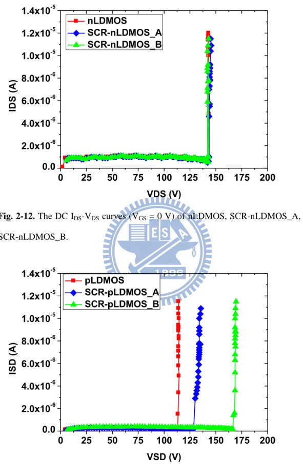
Fig. 2-12 The DC IDS-VDS curves (VGS = 0 V) of nLDMOS,
SCR-nLDMOS_A, and SCR-nLDMOS_B 23
Fig. 2-13 The DC ISD-VSD curves (VSG = 0 V) of pLDMOS,
SCR-pLDMOS_A, and SCR-pLDMOS_B 23
Fig. 3-1 The equivalent circuit of the human body model ESD event [21] 26
Fig. 3-2 Definition of the HBM pulse decay time (td) [21] 26
Fig. 3-3 The equivalent circuit of the machine model ESD event [22] 27
wire [22] 27 Fig. 3-5 The equivalent circuit of the charged device model ESD event [23] 29
Fig. 3-6 The waveforms of a 2-kV HBM ESD stress, 200-V MM ESD
stress, and a 1-kV CDM ESD stress 29
Fig. 3-7 The equivalent circuit of the TLP system 30
Fig. 3-8 The I-V curve measured by 100-ns TLP system 31
Fig. 3-9 The ESD protection design window of HV ESD protection devices
[25] 32
Fig. 3-10 (a) PS-mode, (b) NS-mode, (c) PD-mode, and (d) ND-mode, ESD
test on I/O pins 33
Fig. 3-11 The internal ESD damage due to the pin to pin ESD stress 34
Fig. 3-12 The pin-to-pin ESD test of (a) positive mode and (b) negative-mode 34
Fig. 3-13 The internal ESD damage due to the VDD-to-VSS ESD stress 35
Fig. 3-14 The VDD-to-VSS ESD tests of (a) positive mode and (b)
negative-mode 35
Fig. 3-15 The CDM ESD tests of (a) positive mode and (b) negative-mode 36
Fig. 3-16 TLP-measured results of (in circular symbol) nLDMOS and (in
square symbol) circular_nLDMOS 38
Fig. 3-17 TLP-measured results of (in square symbol) nLDMOS, (in diamond symbol) SCR-nLDMOS_A, and (in triangular symbol)
SCR-nLDMOS_B 39
Fig. 3-18 TLP-measured results of (in square symbol) pLDMOS, (in diamond symbol) SCR-pLDMOS_A, and (in triangular symbol)
SCR-pLDMOS_B 39
Fig. 3-19 SEM images of typical nLDMOS which suffers from a 0.5-kV
HBM ESD stress 43
Fig. 3-20 SEM images of typical circular_nLDMOS which suffers from a
0.5-kV HBM ESD stress 44
Fig. 3-21 SEM images of typical SCR-nLDMOS_A which suffers from a
6-kV HBM ESD stress 44
Fig. 3-22 SEM images of typical SCR-nLDMOS_B which suffers from a
0.5-kV HBM ESD stress 45
Fig. 3-23 SEM images of typical pLDMOS which suffers from a -0.5-kV
HBM ESD stress 45
Fig. 3-24 SEM images of typical SCR-pLDMOS_A which suffers from a
-3.5-kV HBM ESD stress 46
Fig. 3-25 SEM images of typical SCR-pLDMOS_B which suffers from a
Fig. 3-26 The failure current under different channel width (W) for nLDMOS 49 Fig. 3-27 The failure current under different channel width (W) for pLDMOS 49 Fig. 3-28 The failure current under different Drift length (D) for nLDMOS 50
Fig. 3-29 The failure current under different Y for nLDMOS 50
Fig. 3-30 The failure current under different Y for pLDMOS 51
Fig. 3-31 The parasitic current path and resistor in (a) SCR-nLDMOS_A and
(b) SCR-pLDMOS_A 52
Fig. 3-32 The failure current under different Y for SCR-nLDMOS_A 52
Fig. 3-33 The failure current under different spacing between the N+ and P+ at
drain region (Td) for SCR-nLDMOS_A 53
Fig. 3-34 The failure current under different spacing between the N+ and P+ at
source region (Ts) for SCR-pLDMOS_B 53
Fig. 4-1 Forward bias safe operating area (meshed region) [8] 57
Fig. 4-2 Maximum allowable power dissipation versus device-case
temperature [28] 58
Fig. 4-3 The test circuit of eSOA 59
Fig. 4-4 The I-V characteristics measured by 100-ns TLP system. The 100-ns eSOA boundary is shown in orange color and circular
symbol 60
Fig. 4-5 The I-V characteristics measured by 200-ns TLP system. The 200-ns eSOA boundary is shown in orange color and circular
symbol 60
Fig. 4-6 The comparison of eSOA with different pulse width of TLP 61
Fig. 4-7 The test circuit of unclamped inductive switch [30] 64
Fig. 4-8 The waveform of unclamped inductive switch 65
Fig. 4-9 The circuit trajectory of unclamped inductive switch. The unstable
state is (a) inside and (b) outside the boundary of eSOA 65
Fig. 4-10 The waveform of inductive current with different power supply
(Vcc) 66
Fig. 4-11 The inductive current with different power supply (Vcc) 66
Fig. 4-12 The waveform of inductive current with different pulse width (Tp) 67
Fig. 4-13 The inductive current with different pulse width (Tp) 67
Fig. 4-14 The waveform of inductive current with different inductive
impedance (Lext) 68
Fig. 4-15 The inductive current with different inductive impedance (Lext) 68
Fig. 4-16 The waveform of UIS when device is failed 69
Fig. 4-17 The maximum allowable UIS Iswitch,max with different inductive
Fig. 4-18 The waveform of drain voltage (Vds) with different gate bias (Vgs)
during UIS stress 71
Fig. 4-19 The waveform of drain current (Ids) with different gate bias (Vgs)
during UIS stress 71
Fig. 4-20 The waveform of drain voltage (Vds) with different samples whose
device structure and layout parameters are the same during UIS
stress 72
Fig. 4-21 The waveform of drain current (Ids) with different samples whose
device structure and layout parameters are the same during UIS
stress 72
Fig. 4-22 The 100-ns eSOA with different device structure 74
Fig. 4-23 The UIS waveform of typical (a) nLDMOS, (b) circular_nLDMOS,
(c) SCR-nLDMOS_A, and (d) SCR-nLDMOS_B 75
Fig. 5-1 The test circuit of clamped inductive switch [1] 78
Fig. 5-2 The diagram of waveform during the CIS stress 78
Fig. 5-3 The waveform of (a) UIS and (b) CIS 79
Fig. 5-4 The test circuit of UIS with (a) one diode, (b) two diodes, and (c)
three diodes 79
Fig. 5-5 The waveform of drain current with different number of diode
during the CIS stress 79
Fig. 5-6 The cross-sectional view of nLDMOS with buried body which is
shown in red rectangle [2] 80
Fig. 5-7 The 100-ns eSOA with and without buried body [2] 81
Fig. 5-8 (a) The cross-sectional view along A-A’ line and (b) the layout top view of the nLDMOS with the polybending layout arrangement [3] 82
Chapter 1
Introduction
1.1 Motivation
Recently, the high-voltage (HV) technology is prospering due to its extremely extensive applications such as power management integrated circuits (ICs), automotive electronics, light-emitting diode (LED) and liquid-crystal-display (LCD) driver ICs. The higher breakdown voltage and the higher speed are popular achievements in HV applications [5]-[7]. However, the importance of reliability issue should not be underestimated in HV ICs as a result of stringent operating environments. Furthermore, electrostatic discharge (ESD) protection and safe operating area (SOA) have been essential issues of reliability for HV ICs [8]-[10]. The incident of ESD takes place by accident. On the other hand, SOA is concerned about the reliability during normal circuit operating conditions. The HV transistors simultaneously exhibits excellent ESD robustness and wide SOA is preferable to minimize the total chip area; hence, it is importance to have a deeper investigation on the reliability issue of ESD and SOA. ESD design rules are usually not accepted for the purpose of minimizing the device area; therefore, the self-protected HV ICs against ESD stress is popular in HV applications. The insertion of SCR to lateral double-diffused MOS (LDMOS) is an effective technique in improving the ESD robustness [11]; however, the influence of inserting SCR on SOA is seldom referred. As a result, the deeper research concerning the influence of the embedded SCR structure on SOA is important for LDMOS.
1.2 Investigation on the Impact of Junction Curvature Effect
on HV ICs
The influence of curved P/N junction on breakdown voltage is considerable. To predict the breakdown characteristics of curved-abrupt P/N junctions, the junction curvature effect is discussed in this chapter [12]-[14]. The P+/N-well junction is formed by implanting impurities of p-type into N-well through windows in an impervious masking layer. To activate the impurities of p-type, the thermal process is needed. High temperature results in the diffusion of impurities. Hence, the curved junction is formed as illustrated in Fig. 1-1 where rj represents the radius of
metallurgical junction, xj represents the distance from surface of silicon to the
metallurgical junction, rd is the radius of outer depletion boundary, xd is the distance
from surface of silicon to the outer depletion boundary. If the shape of masking layer is rectangle as illustrated in Fig. 1-2, the cylindrical curved junction is formed at the edge of mask and the spherical curved junction is formed at the corner of mask. The junction will avalanche breakdown if the junction is reversed bias. The following equations are derived to analysis the relation between avalanche breakdown voltage (BVdss) and rj.
Mask
Mask
90 90 90 90P
+N-well
Depletion region
x
dr
jr
dx
jFig. 1-2. The 3-D diagram of curved P+/N-well junction [13].
The potential (V) and the electric field (E) in a P/N junction can be calculated from the Poisson’s equation, as shown in equation (1.1) [12].
2 2 ) ( 1 dr V d dr E r d r n n (1.1)
where is the permittivity of silicon and is the space charge density. n = 0 for parallel-plane junction, n = 1 for cylindrical-junction, and n = 2 for spherical-junction. Hence, the electric field (E) and potential (V) can be written as equation (1.2) and (1.3). In addition, the space charge density of abrupt junction is given by equation (1.4). n ' r r n n r c dr r r ) ' r ( E d
1 (1.2)
r' rj Edr ) ' r ( V (1.3) B qN ) r (
(1.4)For parallel-plane junction (n = 0), the electric field and potential can be written as equation (1.5) and (1.6) by replacing the with –qNB.
c ) x x ( qN ) x ( E B d (1.5) ) x x ( x qN ) x x ( qN ) x ( V B d j j B 2 2 2 (1.6)
For cylindrical-abrupt junction (n = 1), the electric field and potential can be written as equation (1.7) and (1.8) by replacing the with –qNB.
r c r ) r r ( qN ) r ( E B d 2 2 2 (1.7) )] r r ln( r ) r r ( [ qN ) r ( V j d j B 2 2 2 2 2 (1.8)
For spherical-abrupt junction (n = 2), the electric field and potential can be written as equation (1.9) and (1.10) by replacing the with –qNB.
2 2 3 3 3 r c r ) r r ( qN ) r ( E B d (1.9) ) r r ( c )] r r ( r ) r r ( [ qN ) r ( V j j d j B 1 1 1 1 2 3 3 2 2 (1.10)
To simplify the calculation, the cylindrical-abrupt and spherical-abrupt junctions are transferred to parallel-plane abrupt junction through Neq and Weq [14]. Neq is the
background doping concentration of equivalent parallel-plane abrupt junction. Weq is
assumptions shown as following to obtain Neq and Weq.
(1) The original and equivalent junctions are in the avalanche breakdown state. (2) The total net charge in the depletion region is conserved during breakdown. (3) The voltage is conserved during breakdown.
As a result, the Emax and BVdss can be respectively written as equation (1.11) and
(1.12) [14]. eq eq max W qN E (1.11) 2 2 eq eq dss W qN BV (1.12)
The maximum electric field is located at the metallurgical junction while the maximum potential is located at the depletion outer boundary. For cylindrical-abrupt junction, combining the equation (1.7) and (1.11), the Emax can be written as equation
(1.13); combining the equation (1.8) and (1.12), the BVdss can be written as equation
(1.14) for cylindrical junction. Similarly, the Emax and BVdss can be respectively
written as equation (1.15) and (1.16) for spherical junction.
eq eq j j d B j max W qN r ) r r ( qN ) r ( E E 2 2 2 (1.13) 2 2 2 2 2 2 2 eq eq j d d d j B d dss W qN )] r r ln( r ) r r ( [ qN ) r ( V BV (1.14) eq eq j j d B j max W qN r ) r r ( qN ) r ( E E 2 3 3 3 (1.15)
2 1 1 2 3 2 3 2 2 eq eq d j d d j B d dss W qN )] r r ( r ) r r ( [ qN ) r ( V BV (1.16)
According to the assumption (1), the relation between Neq, Weq, and BVdss is
given as equation (1.17) and (1.18) [12].
) 7 8 ( 11 10 3 . 9 eq eq W N (1.17) ) ( eq dss . N BV 641013 34 (1.18)
It is necessary to solve the combinational group of equation (1.13), (1.14) and (1.17) to get Neq, Weq, and rd with given NB and rj for cylindrical-abrupt junction.
BVdss is calculated by equation (1.18) and Neq. For spherical-abrupt junction, we can
get the Neq, Weq, rd, BVdss by equation (1.15), (1.16), (1.17), and (1.18). Fig. 1.3
demonstrates the calculating value of breakdown voltage with different rj and NB for
cylindrical-abrupt junction and parallel-plane junction; likewise, Fig. 1.4 demonstrates that for spherical-abrupt junction and parallel-plane junction. It is observed that the breakdown voltage of cylindrical-abrupt junction and spherical-abrupt junction approaches that of parallel-plane junction with longer rj. In other words, the curved
junction is similar to parallel-plane junction when the radius of metallurgical junction is large enough. With the same rj and NB, parallel-plane junction exhibits the largest
BVdss while the BVdss of spherical-abrupt junction is the smallest. In other words, the
spherical-abrupt junction is prone to breakdown among the junctions discussed above. Furthermore, BVdss decrease with decreasing rj both for cylindrical-abrupt and
spherical-abrupt junctions. As a result, the radius of spherical-abrupt junction dominates the BVdss for HV transistors.
Fig. 1-3. The avalanche breakdown voltage versus background doping concentration
for different rj of the cylindrical-abrupt junction [14].
Fig. 1-4. The avalanche breakdown voltage versus background doping concentration
1.3 Thesis Organization
The chapter 1 of this thesis is the motivation of the research and the introduction of junction curvature effect.
The chapter 2 of this thesis includes the device structure of standard LDMOS and the modified LDMOS which is studied in the work. The experimental results comprise the DC IDS-VDS characteristics and the avalanche breakdown voltage.
The chapter 3 of this thesis introduces ESD events and ESD test methods. The experiment includes the TLP, MM, HBM, and failure analysis. The ESD performance with different device structures is discussed, and the causing of poor ESD robustness is discovered according to the failure analysis.
The chapter 4 of this thesis investigates the measured methods and properties of safe operating area (SOA). The classification of SOA is concisely introduced in the chapter. The characteristic of unclamped inductive switch (UIS) is investigated in detail. The experimental results include electrical SOA and UIS for standard nLDMOS and modified nLDMOS. The causing of wide eSOA and excellent UIS level is discussed.
The chapter 5 of this thesis refers to the methods to improve the SOA without paying for the poor ESD robustness.
In the end of this thesis, a short conclusion and future work are given in the chapter 6.
Chapter 2
Proposed Device Structure Designs of LDMOS
2.1 The Standard Device Structure of LDMOS
Fig. 2-1 shows the cross-sectional view of LDMOS which is realized in a 0.5-m 100-V SOI BCD process. The depth of buried oxide is 2 m, gate oxide is 15 nm, field oxide is 570 nm, and active region is 3 m. The devices are separated from each other by trench isolation and buried oxide which can minimize the device area. To prevent the current from concentrating at the device surface, the sheet resistance of PM is larger than HV N-Well to disperse the current. According to the principle of RESURF, HV N-Well is fully depleted with the aid of PM, buried oxide, and P-sub [15] [16].
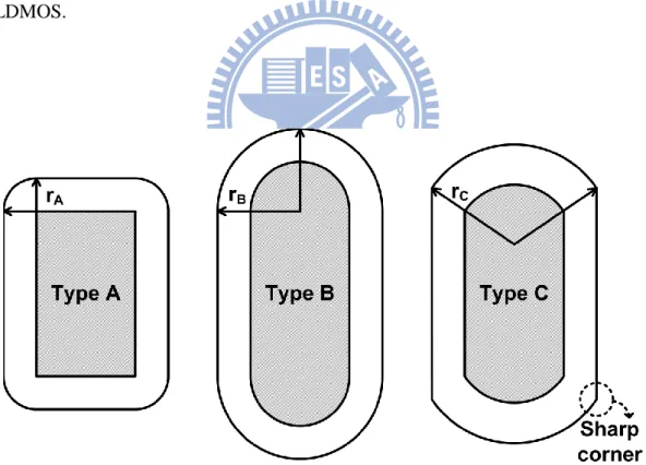
Radius of spherical P/N junction dominates the breakdown voltage according the curvature junction effect [12]-[14]. Fig. 2-2 shows three types of mask results in different radius of spherical P/N junction. Region in gray color represent the mask and outer region represents the junction after diffusion. The shape of mask in type A is a rectangle and the spherical P/N junctions with the smallest radius (rA) are formed at
the corner. The shape of mask in type B is a rectangle with half circle at top and bottom. In this thesis, the substitutive name of shape in type B is elliptic shape. The radius of spherical P/N junction in type B (rB) is medium. The shape of mask in type
C is a rectangle with one third of circle at top and bottom. The radius of spherical P/N junction of type C (rC) is the longest, but the electric charges accumulates at the sharp
corner which lead to a reduction of avalanche breakdown voltage. In conclusion, the shape of mask in type B has the highest avalanche breakdown voltage. Fig. 2-3 shows
the proposed layout styles of LDMOS. In this thesis, the LDMOS are in elliptic layout style except for circular_nLDMOS. The definitions of layout parameters are shown in Fig. 2-1 and Fig. 2-3. W is the channel width. The channel width of circular_nLDMOS is 2r. D represents the drift length. e is the clearance between the contact edge and the center of circle. x is the clearance between the contact and the FOX at drain region while s is the clearance between the contact and the polygate at source region.
(a)
(c)
Fig. 2-1. The cross-sectional view of (a) nLDMOS, (b) circular_nLDMOS, and (c)
pLDMOS.
(a) (b)
(c)
Fig. 2-3. Top view of (a) nLDMOS (b) pLDMOS in elliptic shape and (c)
The field oxide (FOX) under the poly gate plays an important role [17]. Fig. 2-4 demonstrates P/N junction below gate oxide under the condition of reversed bias. Wd
is the depletion width of P/N junction and tox is the thickness of oxide. Electric filed is
shown in dashed line with arrow. For tox < Wd, the maximum electric filed occurs in
the oxide and the oxide would be catastrophically damaged when the maximum electric field is equal to critical electric field. Numerical analysis has shown that the avalanche breakdown occurs in the oxide for Wd/tox higher than 12 [18]. As a result,
the FOX is utilized to keep the ratio lower than 12 for LDMOS.
tox VGS=0V V,P-sub ~0V Ex Ey V,HV N-Well ~VDS ++ +++ Wd (a) VSG=0V V,N-well ~VSD Ex Ey V,P-sub ~0V ++ +++ Wd tox (b)
Fig. 2-4. The P/N junction of (a) nLDMOS and (b) pLDMOS below gate oxide under
the condition of reversed bias: (a) VDS > 0 V and VGS = 0 V. (b) VSD > 0 V and VSG =
0 V.
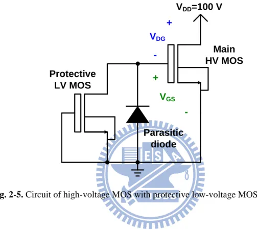
The operating voltage of drain to source (VDS) is 100 V and the operating voltage
of gate to source (VGS) is 5 V. To consider the gate-oxide reliability, the voltage across
drain and gate (VDG) can’t be higher than VDD for a long time. The protective
(HV MOS) form damage, as illustrated in Fig. 2-5. If VDG is accidentally higher than
VDD, the parasitic diode of LV MOS will turn on and clamp VDS to VDD. The parasitic
diode of LV MOS doesn’t affect the normal operation of HV MOS because it is off during normal operation.
+ -VDG VDD=100 V + -VGS Main HV MOS Protective LV MOS Parasitic diode
Fig. 2-5. Circuit of high-voltage MOS with protective low-voltage MOS.
2.2 The Device Structure of LDMOS with embedded SCR
The insertion of silicon controlled rectifier (SCR) to MOS is a popular technique to improve ESD robustness [11]. Fig. 2-6 shows the LDMOS with embedded SCR. SCR-nLDMOS and SCR-pLDMOS respectively represents the n-type and p-type LDMOS with embedded SCR. The current path of SCR and BJT are respectively located at the side and the center of drain region for SCR-LDMOS_A, as illustrated in Fig. 2-6 (a) and (c). SCR-LDMOS_B alters the relative position of N+ and P+ at drain region, so the orientation of BJT and parasitic SCR is changed as illustrated in Fig. 2-6 (b) and (d). The influence of the embedded SCR structures on the ESD and SOA of LDMOS is one of the important topics in the thesis. The definitions of layoutparameters are shown in Fig. 2-6. The definitions of W, D, and e are the same as illustrated in Fig. 2-1 and Fig. 2-3. z is the clearance between the contact and the FOX at drain region for SCR-nLDMOS. s is the clearance between the contact and the polygate at source region for SCR-nLDMOS. The similar definitions of SCR-pLDMOS are illustrated in Fig. 2-6 (c) and Fig. 2-6 (d).
(a) (b)
(c) (d)
Fig. 2-6. The cross-sectional view of (a) SCR-nLDMOS_A (b) SCR-nLDMOS_B (c)
2.3 I
DS-V
DSCharacteristics
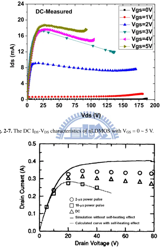
Fig. 2-7 demonstrates the DC IDS-VDS characteristics of nLDMOS with W = 40
m, L = 2 m, D = 12 m, Y = 13 m, x = 6 m, s = 1 m, and e = 2 m. The gate bias voltage is varied from 0 V to 5 V. The higher VGS results in higher IDS at the same
VDS. However, the negative differential output resistance is observed at high VDS
region. It was reported that the reduction of IDS at high VDS region arose from
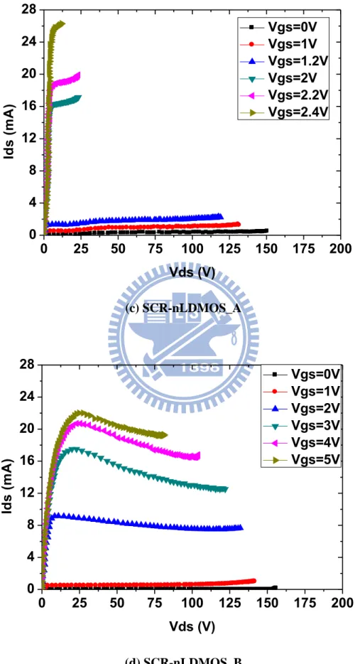
self-heating effect [19]. At saturation region, the carriers are travelling at the saturated velocity in the drift region. The lattice temperature increases as a result of power dissipation. The high lattice temperature causes a severe degradation of carrier mobility [20]; hence, the travelling velocity is smaller. As a result, the drain current decreases with increasing drain voltage. Fig. 2-8 shows the IDS-VDS characteristics of
a SOI LDMOS with the 50-m drift length, the 0.2-m silicon thin-film, the 1.2-m buried oxide, and the 0.3-mm2 device area [19]. The experimental results reveal that the self-heating effect is serious under DC condition while it is unapparent under 2-s power pulse condition. It is due to the higher lattice temperature which results from higher power dissipation under DC condition.
Fig. 2-9 and Fig. 2-10 demonstrate the DC IDS-VDS characteristics of all typical
HV DMOS whose layout parameters are listed in Table 2.1. The range of gate bias is from 0 V to 5 V. SCR-nLDMOS_A tends to snapback at small VDS when the gate bias
is larger than 2.4 V, so the measurement is done under the condition of VGS=0 V~2.4 V.
Because the mobility of N-type carrier is larger than that of P-type carrier in nature, the drain current of N-type DMOS are larger than that of P-type DMOS at the same absolute value of VGS.
Fig. 2-7. The DC IDS-VDS characteristics of nLDMOS with VGS = 0 ~ 5 V.
Fig. 2-8. The IDS-VDS characteristics of a SOI LDMOS transistor. Solid line:
simulated curve without self-heating effect. Dotted line: calculated curve which take self-heating effect into account. Experimental data which are measured under the 2-s, 100-s power pulses, and DC conditions [19].
0 25 50 75 100 125 150 175 200 0 4 8 12 16 20 24 Id s ( m A ) Vds (V) Vgs=0V Vgs=1V Vgs=2V Vgs=3V Vgs=4V Vgs=5V DC-Measured
(a) nLDMOS (b) Circular_nLDMOS 0 25 50 75 100 125 150 175 200 0 4 8 12 16 20 24 28 Id s ( m A ) Vds (V) Vgs=0V Vgs=1V Vgs=2V Vgs=3V Vgs=4V Vgs=5V 0 25 50 75 100 125 150 175 200 225 0 4 8 12 16 20 24 28 Id s ( m A ) Vds (V) Vgs=0V Vgs=1V Vgs=2V Vgs=3V Vgs=4V Vgs=5V
(c) SCR-nLDMOS_A
(d) SCR-nLDMOS_B
Fig. 2-9. The DC IDS-VDS characteristics of N-type typical DMOS.
0 25 50 75 100 125 150 175 200 0 4 8 12 16 20 24 28 Id s ( m A ) Vds (V) Vgs=0V Vgs=1V Vgs=1.2V Vgs=2V Vgs=2.2V Vgs=2.4V 0 25 50 75 100 125 150 175 200 0 4 8 12 16 20 24 28 Id s ( m A ) Vds (V) Vgs=0V Vgs=1V Vgs=2V Vgs=3V Vgs=4V Vgs=5V
(a) pLDMOS (b) SCR-pLDMOS_A -200 -175 -150 -125 -100 -75 -50 -25 0 -2.4 -2.0 -1.6 -1.2 -0.8 -0.4 0.0 Id s ( m A ) Vds (V) Vsg=0V Vsg=1V Vsg=2V Vsg=3V Vsg=4V Vsg=5V -200 -175 -150 -125 -100 -75 -50 -25 0 -2.4 -2.0 -1.6 -1.2 -0.8 -0.4 0.0 Id s ( m A ) Vds (V) Vsg=0V Vsg=1V Vsg=2V Vsg=3V Vsg=4V Vsg=5V
(c) SCR-pLDMOS_B
Fig. 2-10. The DC IDS-VDS characteristics of P-type typical DMOS.
TABLE 2.1
The layout parameters of typical DMOS
Typical Device Structure Layout Parameters (m) nLDMOS W = 40, L = 2, D = 12, Y = 13, x = 6, s = 1, and e = 2. Circular_nLDMOS r = 23, L = 2, D = 12, Y = 23, x = 6, and s = 1. SCR-nLDMOS_A W = 40, L = 2, D = 12, Y = 7, z = 3, s = 1, e = 2, and Td = Ts = 0. SCR-nLDMOS_B W = 40, L = 2, D = 12, Y = 7, z = 3, s = 1, e = 2, and Td = Ts = 0. pLDMOS W = 40, L = 2, D = 12, Y = 13, x = 6, s = 1, and e = 2. SCR-pLDMOS_A W = 40, L = 2, D = 12, Y = 3, z = 1, s = 1, e = 2, and Td = Ts = 0. SCR-pLDMOS_B W = 40, L = 2, D = 12, Y = 3, z = 1, s = 1, e = 2, and Td = Ts = 0. -200 -175 -150 -125 -100 -75 -50 -25 0 -2.4 -2.0 -1.6 -1.2 -0.8 -0.4 0.0 Id s ( m A ) Vds (V) Vgs=0V Vgs=1V Vgs=2V Vgs=3V Vgs=4V Vgs=5V
2.4 Avalanche Breakdown Voltage
The definition of avalanche breakdown voltage (BVdss) is the drain voltage when
the drain current is equal to 10 A under the condition of VGS = 0 V. The following
shows the BVdss of typical HV DMOS whose parameters are listed in Table 2.1. Fig.
2-11and Fig. 2-12 demonstrate the IDS-VDS curves with VGS = 0 V for n-type HV
DMOS; similarly, Fig. 2-13 shows the ISD-VSD curves with VSG = 0 V for p-type HV
DMOS. First of all, Fig. 2-11 reveals that the BVdss of circular_nLDMOS is larger
than that of nLDMOS. Secondly, Fig. 2-12 exhibits that the BVdss of nLDMOS,
SCR-nLDMOS_A, and SCR-nLDMOS_B are almost identical. Finally, Fig. 2-13 manifests that the BVdss of SCR-pLDMOS_A is the highest while the BVdss of
pLDMOS is the lowest. Table 2.2 lists the BVdss and radius of spherical P/N junction
with different device structure. The radius of spherical P/N junction dominates the BVdss [12]-[14]; therefore, BVdss increases with increasing radius.
Fig. 2-11. The DC IDS-VDS curves of nLDMOS and circular_nLDMOS (VGS = 0 V).
0 25 50 75 100 125 150 175 200 0.0 2.0x10⁻⁶ 4.0x10⁻⁶ 6.0x10⁻⁶ 8.0x10⁻⁶ 1.0x10⁻⁵ 1.2x10⁻⁵ 1.4x10⁻⁵ ID S ( A ) VDS (V) nLDMOS Circular_nLDMOS
Fig. 2-12. The DC IDS-VDS curves (VGS = 0 V) of nLDMOS, SCR-nLDMOS_A, and
SCR-nLDMOS_B.
Fig. 2-13. The DC ISD-VSD curves (VSG = 0 V) of pLDMOS, SCR-pLDMOS_A, and
SCR-pLDMOS_B. 0 25 50 75 100 125 150 175 200 0.0 2.0x10⁻⁶ 4.0x10⁻⁶ 6.0x10⁻⁶ 8.0x10⁻⁶ 1.0x10⁻⁵ 1.2x10⁻⁵ 1.4x10⁻⁵ ID S ( A ) VDS (V) nLDMOS SCR-nLDMOS_A SCR-nLDMOS_B 0 25 50 75 100 125 150 175 200 0.0 2.0x10⁻⁶ 4.0x10⁻⁶ 6.0x10⁻⁶ 8.0x10⁻⁶ 1.0x10⁻⁵ 1.2x10⁻⁵ 1.4x10⁻⁵ IS D ( A ) VSD (V) pLDMOS SCR-pLDMOS_A SCR-pLDMOS_B
TABLE 2.2
The avalanche breakdown voltage of typical DMOS
Typical Device Structure
Radius of Spherical P/N Junction (m) Avalanche Breakdown Voltage (V) nLDMOS 17.0 143.0 Circular_nLDMOS 21.0 183.0 SCR-nLDMOS_A 18.5 145.0 SCR-nLDMOS_B 16.0 142.0 pLDMOS 19.0 114.5 SCR-pLDMOS_A 20.0 134.0 SCR-pLDMOS_B 22.0 168.5
Chapter 3
Introduction to Electrostatic Discharge and
Experimental Results
3.1 Introduction to Electrostatic Discharge (ESD)
ESD is an instantaneous discharging of electrostatic charges on IC pins. It take place under the situations such as a physical touch of a human body and an IC products, contact of manufacturing machines and wafers, or discharge of secondhand induced electrical field on an IC chips. According to the different discharge conditions and sources of electrostatic charges, ESD can be classified to human-body model (HBM), machine-model (MM), and charged-device model (CDM).
3.1.1 Human Body Model (HBM)
HBM is a common ESD event that arose from the contact of a charged human body and an IC product. The friction between human body and an object results in the charged human body, thus the electrostatic charge transfers into the IC products when the charged human body touches the IC products. To prevent the catastrophically failure on IC products, the human body model is established to simulate this kind of ESD event and quantify the IC robustness against the HBM ESD event. The equivalent circuit for HBM ESD event is shown in Fig. 3-1 [21], where the 1.5-k resistor and the 100-pF capacitor represent the equivalent parasitic resistor and capacitor of a human body. The DUT represents the device under test. The HBM design eliminates the weak ESD protection designs and protects the susceptible devices. Commercial ICs are generally demanded to pass 2-kV HBM ESD stress at
least, which can generate ESD current with a peak value about 1.3 A and a rise time about 10 ns. Fig. 3-2 shows the typical HBM ESD waveform generated by the ESD HBM tester to a short wire [21]. In particular, most of the HBM ESD energy is concentrate on the time interval between 0 ns to 100 ns.
High-Voltage
Pulse
Generator
DUT
Socket
100pF
1.5k
S1
S2
Fig. 3-1. The equivalent circuit of the human body model ESD event [21].
3.1.2 Machine Model (MM)
The MM ESD event arose from the contact of a machine and IC products. The equivalent circuit diagram of MM ESD event is shown in Fig. 3-3 [22], where there is no equivalent resistor on the equivalent discharging path because the electrostatic charge source is charged machine with 0-resistor.
High-Voltage
Pulse
Generator
DUT
Socket
200pF
S1
S2
10k
~10M
Fig. 3-3. The equivalent circuit of the machine model ESD event [22].
Fig. 3-4 shows the waveform of a 400-V MM ESD pulse generated by the MM ESD tester [22]. A commercial IC product is generally required to pass at least 200-V MM ESD stress, which can generate an ESD current with a peak value about 3.5 A and a rise time about 10 ns. The MM ESD level of a semiconductor device is generally 8 ~ 12 times smaller than its HBM ESD level due to the faster rise time and voltage resonance of a MM ESD pulse.
3.1.3 Charged Device Model (CDM)
The CDM ESD event happens under the condition of the contact of charged IC and external grounded object. The IC is charged through the mechanism of electrostatic induction, and most of the CDM charges are initially stored in the body (the p-substrate) of a CMOS IC. When one or more pins of this charged IC is touched by an external grounded object, CDM charges in the p-substrate will be discharged from the IC inside to the grounded object outside. There is no standard equivalent parasitic capacitor and resistor for the CDM ESD stress because different dimension of chips, different form and size of packages result in different values of the parasitic capacitor and resistor of IC chips. Fig. 3-5 shows the simplified CDM test circuit. Rd,
Ld and Cd represents the equivalent parasitic resistor, inductor and capacitance of DUT.
The DUT is initially charged through the large resistor Rg with relatively small current,
and then DUT contact the grounded object and discharge immediately. A commercial IC is generally requested to pass at least 1-kV CDM ESD stress, which can generate an ESD current with peak current value about 15 A within a rise time less than 200 ps [23]. Fig. 3-6 makes a contrast with the waveforms of a 2-kV HBM ESD stress, a 200-V MM ESD stress, and a 1-kV CDM ESD stress which has 4-pF equivalent capacitor of the device under test. Table 3.1 shows the commercial specification for the HBM, MM and CDM level.
V
ESDRg
Rd
Ld
Cd
Device
Under
Test
Fig. 3-5. The equivalent circuit of the charged device model ESD event [23].
Fig. 3-6. The waveforms of a 2-kV HBM ESD stress, 200-V MM ESD stress, and a
TABLE 3.1
The commercial specification for the HBM, MM and CDM level.
HBM (kV) MM (V) CDM (kV)
Okay +/- 2 +/- 200 +/- 2
Safe +/- 4 +/- 400 +/- 1.5
Super +/- 10 +/- 1000 +/- 2
3.1.4 Transmission Line Pulse (TLP) System
The equivalent circuit of TLP system is shown in Fig. 3-7 The TLP system applied the voltage pulse, which pulse amplitude is Vin and the pulse width is t, to the device under test (DUT). The oscilloscope measured the voltage and current during the TLP stress, and then the source-meter measured the leakage under certain bias condition. Device Under Test To scope RL Vin t Source of energy V I
-+
The steps above are sequentially repeated with increasing TLP pulse amplitude until the device satisfies the failed criteria. In this thesis, the definition of failed criteria is Ileakage > 100* Ileakage, initial, where Ileakage is the leakage current measured after
TLP zapping and Ileakage, initial is the leakage current of fresh transistor. The I-V curve
measured by TLP system is shown in Fig. 3-8. Trigger point represents the triggering of parasitical bipolar junction transistor (BJT). Secondary breakdown current (It2)
represents the maximum allowable current. In other words, the device is judged to failure as the current is higher than It2. Interestingly, the HBM ESD waveform reveals
that the ESD energy is concentrate on the time interval between 0 ns to 100 ns and it is observed that the HBM level is proportional to It2 [24]. With the information
provided by TLP system, IC designers can easy choose the direct device under the guide of design window, as illustrated in Fig. 3-9 [25].
Fig. 3-8. The I-V curve measured by 100-ns TLP system.
0 25 50 75 100 125 150 175 200 0 1 2 3 4 5 610 -11 10-10 10-9 10-8 10-7 10-6 10-5 10-4 10-3 10-2 0 1 2 3 4 5 6 Vt2, It2 Failure criterion Vhold 100ns_TLP Leakage Id s ( A ) Vds (V) Vt1, It1 Id s ( A ) Leakage (A)
Fig. 3-9. The ESD protection design window of HV ESD protection devices [25].
3.2 ESD Test Methods
ESD test has positive and negative type in order to simulate the positive and negative electrical charges in natural environment. Furthermore, IC chip have several input/output (I/O) pins and power pins; therefore, ESD test can occur on different pin combinations. The major pin combinations of ESD test are shown as following.
3.2.1 ESD Test on I/O Pins
The human-body model and the machine-model ESD stress on each I/O pins with the VDD or VSS pins relatively ground are illustrate through Fig. 3-10(a) to 3-10(d) [27], [28]:
(1) PS mode
Positive ESD voltage is applied to the tested I/O pin with VSS pins relatively grounded, as shown in Fig. 3-10(a). VDD pins and all other pins are kept floating during the test.
(2) NS mode
Negative ESD voltage is applied to the tested I/O pin with VSS pins relatively grounded, as shown in Fig. 3-10(b). VDD pins and all other pins are kept floating during the test.
(3) PD mode
Positive ESD voltage is applied to the tested I/O pin with VDD pins relatively grounded, as shown in Fig. 3-10(c). VSS pins and all other pins are kept floating during the test.
(4) ND mode
Negative ESD voltage is applied to the tested I/O pin with VDD pins relatively grounded, as shown in Fig. 3-10(d). VSS pins and all other pins are kept floating during the test.
VDD VSS (a) PS-mode +VESD 0V VDD VSS -VESD 0V (b) NS-mode VDD VSS +VESD 0V (c) PS-mode -VESD 0V VDD VSS (d) ND-mode
Fig. 3-10. (a) PS-mode, (b) NS-mode, (c) PD-mode, and (d) ND-mode, ESD test on
3.2.2 Pin to Pin ESD Test
ESD events would occur on one of the I/O pins with another I/O pin relatively grounded. In other words, power lines are floating during the pin to pin ESD test. The pin to pin ESD test can easily cause ESD damage located at the internal circuits if the ESD protective design is poor. The common pin to pin ESD path is shown in Fig. 3-11. If every two of I/O pins is tested one by one, the ESD test is inefficient and uneconomic. In order to shorten the testing period, ESD stress is applied on the tested I/O pin with all other I/O pins relatively grounded. The pin to pin ESD test is subdivided into positive-mode and negative-mode as illustrated in Fig. 3-12(a) and Fig. 3-12(b). Internal Circuits Input PAD Output PAD +VESD 0V VDD VSS IESD IESD
Fig. 3-11. The internal ESD damage due to the pin to pin ESD stress.
VDD VSS +VESD 0V (a) Positive-mode VDD VSS -VESD 0V (b) Negative-mode
Internal
Circuits
Input PAD Output PADVDD
VSS
IESD +VESD 0V IESDFig. 3-13. The internal ESD damage due to the VDD-to-VSS ESD stress.
3.2.3 VDD-to-VSS ESD Test
The ESD event may happen between two power pins. The internal circuits are vulnerable to ESD stress under the condition that ESD voltage is applied to VDD with VSS relatively ground, as shown in Fig. 3-13. To simulate this kind of ESD-stress condition, a positive or a negative ESD voltage is applied to the VDD pin of an IC chip while VSS pin is relatively grounded, as illustrated in Fig. 3-14(a) and Fig. 3-14(b). VDD VSS +VESD 0V (a) Positive-mode VDD VSS -VESD 0V (b) Negative-mode
VDD
VSS
(a) Positive-mode +VESD
R
VDD
VSS
(b) Negative-mode -VESD
R
Fig. 3-15. The CDM ESD tests of (a) positive mode and (b) negative-mode.
3.2.3 CDM ESD Test
The mechanism of CDM ESD event differs from the HBM and MM ESD events; therefore, the CDM ESD test is especially defined. The substrate of an IC product is initially full of electrostatic charge, and then the device instantaneously discharged when one of the IC pin is ground. In other words, the ESD path is from the inside of IC chip to the outside of grounded object. In order to fill IC substrate with electrostatic charges, the ESD voltage is applied to the VSS pin through the large resistor, as shown in Fig. 3-15(a) and Fig. 3-15(b). With the large resistor, the electrical current is small during charging the device under test, otherwise, the charging current will directly damage the VSS pin and the electrostatic charges will not remain in IC substrate. The ESD voltage is instantly discharged through the pins included the input, output, and VDD pins. To simulate the electrostatic charge in nature, the CDM ESD test is classified into positive-mode and negative-mode, as shown in Fig. 3-15(a) and Fig. 3-15(b).
3.3 Experimental results
First of all, the investigation is focus on the typical HV DMOS as listed in Table 2.1 for the purpose of verifying the effect of different device structures on ESD robustness. Consequently, the following experimental results include TLP, HBM, MM, and failure analysis. The second part is the analysis of ESD robustness with different layout parameters. A brief summary about the ESD robustness of HV DMOS is in the end.
3.3.1 ESD Robustness
The following is the ESD experimental results of typical HV DMOS. Fig. 3-16~18 show the TLP-measured results under the same condition of VGS = 0 V. The
solid line presents the I-V curve while the dotted line is the leakage current which is measured after every TLP ESD stress. The data of Vt1, It1, Vhold, and It2 are extracted
from TLP-measured I-V curve, as illustrated in Table 3.2. The drift length of circular_nLDMOS is longer than that of nLDMOS, so circular_nLDMOS needs higher energy to trigger the parasitic BJT. In other words, the Vt1 and It1 of
circular_nLDMOS are larger than that of nLDMOS. Both nLDMOS and circular_nLDMOS are damaged while entering the snapback region. As a result, the It2 are poor for both devices. The SCR device exhibits the excellent ESD robustness
within small layout area due to its low holding voltage. Accordingly, the insertion of SCR to HV DMOS is applied to improve the ESD robustness. Fig. 3-17 demonstrates that the It2 of SCR-nLDMOS_A is excellent while the It2 of SCR-nLDMOS_B is
almost identical to that of nLDMOS. It is supposed that the triggering of parasitic SCR is failed in SCR-nLDMOS_B. Therefore, the SCR-nLDMOS_B acts like nLDMOS when entering the snapback region. Fig. 3-18 shows the TLP-measured I-V
curve for p-type HV DMOS. Likewise, the SCR-pLDMOS_A exhibits excellent failure current while SCR-pLDMOS_B behaves like pLDMOS which fails while entering the snapback region. Hence, it is supposed that the triggering of parasitic SCR is failed in SCR-pLDMOS_B.
Fig. 3-16. TLP-measured results of (in circular symbol) nLDMOS and (in square
symbol) circular_nLDMOS. 0 25 50 75 100 125 150 175 200 0 1 2 3 410 -11 10-10 10-9 10-8 10-7 10-6 10-5 10-4 10-3 10-2 0 1 2 3 4 Id s ( A ) Vds (V) Circular_nLDMOS nLDMOS
leakage current of circular_nLDMOS leakage current of nLDMOS
Id s ( A ) Leakage (A)
Fig. 3-17. TLP-measured results of (in square symbol) nLDMOS, (in diamond
symbol) SCR-nLDMOS_A, and (in triangular symbol) SCR-nLDMOS_B.
Fig. 3-18. TLP-measured results of (in square symbol) pLDMOS, (in diamond
symbol) SCR-pLDMOS_A, and (in triangular symbol) SCR-pLDMOS_B.
0 25 50 75 100 125 150 175 200 0 1 2 3 4 5 610 -11 10-10 10-9 10-8 10-7 10-6 10-5 10-4 10-3 10-2 10-1 0 1 2 3 4 5 6 Id s ( A ) Vds (V) nLDMOS SCR-nLDMOS_B SCR-nLDMOS_A Leakage of nLDMOS Leakage of SCR-nLDMOS_B Leakage of SCR-nLDMOS_A Id s ( A ) Leakage (A) 0 25 50 75 100 125 150 175 200 0 1 2 3 410 -11 10-10 10-9 10-8 10-7 10-6 10-5 10-4 10-3 10-2 10-1 0 1 2 3 4 Is d ( A ) Vsd (V) pLDMOS SCR-pLDMOS_B SCR-pLDMOS_A Leakage of pLDMOS Leakage of SCR-pLDMOS_B Leakage of SCR-pLDMOS_A Is d ( A ) Leakage (A)
TABLE 3.2
The TLP-measured results of typical HV DMOS.
Typical Device Structure
Vt1 (V) It1 (mA) Vhold (V) It2 (A)
nLDMOS 164.9 14.9 14.4 ~ 0.0149 Circular_nLDMOS 190.0 16.5 13.5 ~ 0.0165 SCR-nLDMOS_A 154.7 10.1 10.5 5.6 SCR-nLDMOS_B 163.9 7.9 27.6 ~ 0.0079 pLDMOS 187.9 107.1 16.4 ~ 0.1071 SCR-pLDMOS_A 126.5 29.6 19.6 2.2 SCR-pLDMOS_B 187.5 43.7 13.1 ~ 0.0437
The common estimation of the ability against the ESD stress includes It2, HBM,
and MM is shown in Table 3.3. The sample size is one for TLP-test and the sample size is three for HBM-test and MM-test. Sample one is simplified as “#1”. Sample two and three are analogically simplified as “#2” and “#3”. The voltage step of HBM-test is 0.5 kV while that of MM-test is 50 V. HBM and MM tests are in positive-mode for n-type DMOS and in negative-mode for p-type DMOS. The HBM level is below 0.5 kV for n-type HV DMOS which fails while entering the snapback region in TLP-test. The MM level is below 50 V for n-type HV DMOS of which the It2 is poor. Likewise, the HBM level is below -0.5 kV and the MM level is below -50
V for p-type HV DMOS which fails while entering the snapback region in TLP-test. On the contrary, the HBM level is 6 kV and the MM level is 200 V for SCR-nLDMOS_A. The HBM level is -3 kV and the MM level is -100 V for SCR-pLDMOS_A. The insertion of SCR to HV DMOS is useful to improve ESD
robustness. Table 3.4 demonstrates the ESD ranking according to It2 per unit device
area. The first price is the SCR-nLDMOS_A and the second price is the SCR-pLDMOS_A which agrees with the results of HBM and MM.
TABLE 3.3
The ESD performance of typical HV DMOS includes It2, HBM, and MM.
Typical Device Structure
It2 (A) HBM (kV) MM (V)
#1 #1 #2 #3 #1 #2 #3 nLDMOS ~ 0.0149 Below 0.5 Below 50 Circular_nLDMOS ~ 0.0165 Below 0.5 Below 50
SCR-nLDMOS_A 5.6 6 6.5 6.5 200 200 300 SCR-nLDMOS_B ~ 0.0079 Below 0.5 Below 50
pLDMOS ~ 0.1071 Below -0.5 Below -50 SCR-pLDMOS_A 2.2 -3 -3.5 -3.5 -100 -100 -150 SCR-pLDMOS_B ~ 0.0437 Below -0.5 Below -50
TABLE 3.4
The ESD ranking of typical HV DMOS.
ESD Ranking Device Structure Device Area (m2) It2 (A) It2/Device Area (mA) 1st place SCR-nLDMOS_A 8380.0 5.6 668.3 2nd place SCR-pLDMOS_A 7990.5 2.2 275.3 3rd place pLDMOS 7783.0 0.1071 13.8 4th place Circular_nLDMOS 5975.0 0.0165 2.8 5th place SCR-pLDMOS_B 7794.0 0.0437 5.6 6th place nLDMOS 7162.0 0.0149 2.1 7th place SCR-nLDMOS_B 7468.0 0.0079 1.1
3.3.2 Failure Analysis
To further support the ESD levels shown in Table 3.3 and the supposition mentioned at 3.3.1, failure analyses on these failed typical HV DMOS is carried out through the way of taking scanning electron microscope (SEM) images. Fig. 3-19 shows the ESD failure locations of nLDMOS which suffers from a 0.5-kV HBM ESD stress. The contacts of drain N+ region are permanently damaged by HBM ESD stress. The catastrophic contact spike of drain N+ region causes the increase in leakage of HV N-well/P-sub junction. The phenomenon is called contact-spike-induced junction leakage. Furthermore, because the finger edge is easily crowded with electron and vulnerable to ESD stress, the damage at finger edge is more serious than that at finger side. Fig. 3-20 shows the ESD failure locations of circular_nLDMOS which suffers from a 0.5-kV HBM ESD stress. The device structure of circular_nLDMOS is identical to that of nLDMOS; hence, the contact spike happens at drain N+ region and the leakage of HV N-well/P-sub junction increases. Besides, the smallest parasitic resistance from drain to source (RDS) is the resistance from the outer contact-ring at
drain region to the contact at source region. Therefore, the ESD current crowds at the outer contact-ring and causes the catastrophic damage at the outer contact-ring. The SEM image of SCR-nLDMOS_A which suffers from a 6-kV HBM ESD stress is illustrated in Fig. 3-21. The contact spike occurs at drain P+ region. The metal of contact causes the HV N-well/P-sub junction short and the leakage increases. Furthermore, because the contact spike is located at the contacts of drain P+ region, the ESD current path is parasitic SCR path as shown in Fig. 2-6 (a). Moreover, the contacts of drain N+ region are intact. That is, the parasitic SCR of SCR-nLDMOS_A effectively bypass the high current during the HBM ESD stress. On the contrary, the contact spike of SCR-nLDMOS_B is located at the drain N+ region, which verifies that the triggering of parasitic SCR is failed for SCR-nLDMOS_B and the ESD
![Fig. 1-3. The avalanche breakdown voltage versus background doping concentration for different r j of the cylindrical-abrupt junction [14]](https://thumb-ap.123doks.com/thumbv2/9libinfo/8761052.208183/21.892.159.724.127.515/avalanche-breakdown-voltage-background-concentration-different-cylindrical-junction.webp)

![Fig. 3-1. The equivalent circuit of the human body model ESD event [21].](https://thumb-ap.123doks.com/thumbv2/9libinfo/8761052.208183/40.892.140.759.276.1102/fig-equivalent-circuit-human-body-model-esd-event.webp)
![Fig. 3-3. The equivalent circuit of the machine model ESD event [22].](https://thumb-ap.123doks.com/thumbv2/9libinfo/8761052.208183/41.892.138.760.313.1074/fig-equivalent-circuit-machine-model-esd-event.webp)
![Fig. 3-5. The equivalent circuit of the charged device model ESD event [23].](https://thumb-ap.123doks.com/thumbv2/9libinfo/8761052.208183/43.892.147.744.97.1084/fig-equivalent-circuit-charged-device-model-esd-event.webp)
