RM02D-2
Ultra-Low-Voltage Mixer and
VCO
in
0.
I8-pm
CMOS
Hsieh-Hung Hsieh, Kuo-Sheng Chung and Liang-Hung Lu
Department of Electrical Engineering and Graduate
Institute
of Electronics Engineering,
National Taiwan University, Taipei, Taiwan, R.O.C.
Abstract - Ultra-low-voltage techniques for RF frontend circuits are presented in this paper, Using a standard 0.18- pm CMOS technology, a down-conversion mixer and a voltage-controlled oscillator were designed and fabricated for
5-GHz wireless applications. With a 5.2-GHz RF signal, the mixer has a conversion gain of 3 dB, while the VCO exhibits a tuning range of 8.9% and a phase noise of -97 dBclHz at 1-
MHz offset. Both circuits operate at a reduced supply voltage of 0.6 V, The power consumptions of the mixer and the VCO are 792 and 696 pW, respectively.
Index Terms - CMOS FW, mixers, voltage controIled oscillators, ultra-low-power, ultra-low-voltage.
I. INTRODUCTION
With recent advances in semiconductor technology, CMOS provides a promising solution for the integration of the
RF
frontend with the baseband circuitry in a single chip. The trend of high-level integration significantly reduces the implementation cost and the operation power of commercial wireless products. Fully integrated wireless transceivers fabricated in CMOS technologies have been reported [1]-[3] for all kinds of wireless applications, such as cellular phones, global positioning systems and wireless local-area-networks. In addition to standard wireless communication systems, the development of ultra-low- power and ultra-low-voltage RF techniques has attracted great attention in recent years due to the emerging applications such as W I D and wireless sensor networks.Because of the required threshold voltage and the inherently low transconductance of the MOSFETs, it is
extremely difficult to operate RF frontend circuits with a reduced supply voltage and power dissipation, especially for multi-gigahertz applications. Using a standard 0.1
X-
pm CMOS technology, a down-conversion mixer and a VCO are presented to demonstrate the potential of CMOS frontend circuits for low-power and low-voltage operation. With the proposed topoIogies, the fabricated circuits operate at a reduced supply voltage of 0.6 V with a power consumption less than 1 mW while maintaining reasonable performance at 5-GHz frequency band.
Section 11 of this paper presents the proposed circuit topologies of the mixer and the VCO. The experimental results of the fabricated circuits are shown in Section 111.
-r"m
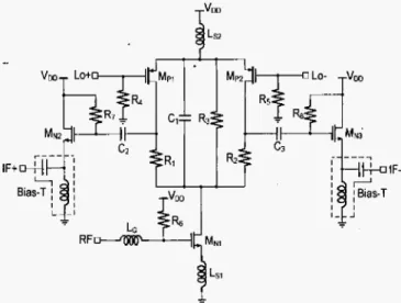
Fig. 1. Schematic ofthe ultra-low-voltage mixer.
Finally, a conclusion is provided in Section IV of this paper.
11. CIRCUIT DESTGN A. Down-Conversion Mixer Topology
Figure 1 shows the schematic of the proposed down- conversion mixer with all on-chip components. In order to achieve the highest possible conversion gain with
a
reduced supply voltage and power dissipation, a folded single-balanced mixer topology with a current bleeding technique is employed. As shown in Fig. 1, MNI is used as the input stage for theRF
signal, while Mpl and MPZ act as the switching pair driven by the LO signals. The RFcurrent generated by the transconductance of MN1 is directed to the source of the switching pair through the bypass capacitor C,, providing frequency conversion of the single-balanced mixer. In this design, resistors R I and
R2 are used as the loads of the switching pair. The values of the resistive loads are chosen to maximize the conversion gain. Due to the supply voltage limitation, a current bleeding technique provided by R3 is employed. As part of the bias current flows through
R3,
large voltage0-7803-89S3-2/05/$20.00 0 2005 IEEE
167
4
Fig. 2 . Schematic of the ultra-low-voltage VCO.
headroom. required by R I and
R2
can be prevented,. allowing low-voltage operation of the mixer. To improve the gain and impedance matching for the RF input, inductive source degeneration technique (Lsl and LG) is adopted for the input transistor MNI. At the IF outputs, open-source buffers ( M N ~ and MN3) are used to drive the 50-11 instruments for the measurement purposes.The folded single-balanced mixer is biased with the
gate of MNI connected to Vno and the gate of Mpl and MPZ tied to the ground through resistors. It is observed that optimized conversion gain can be achieved when all transistors are biased in saturation region. From the dc analysis, the supply voltage, Van, should be kept approximately between Vth and 2Vth, where Vth is the threshold voltage of the MOSFETs. Therefore, the proposed circuit topology is suitable for ultra-low-voltage applications.
B. VCO Topology
The cross-coupled LC-tank topology is widely used for
VCO designs at radio frequencies. With reasonable Q- factors of on-chip passive components, low power consumption and low phase noise can be achieved in a standard CMOS technology. However, the performance of conventional cross-coupled VCOs degrades significantly as the supply voltage decreases. The implementation of a multi-gigahertz VCO with a reduced supply voltage and power consumption is still a challenge.
Figure 2 shows the schematic of the ultra-low-voltage
VCO. In order to reduce the required supply voltage, the current source is eliminated from the conventional VCO topology. The negative resistance is provided by the cross-connection of M I and M2 in positive feedback, while the tank is established by the spiral inductors (LI, L2) and the varactors ( C l , C,). Open-drain buffer stages, M3 and
MA, are also included to drive the external 5 0 - 0 Load of
the test instruments.
111. EXPERIMENTAL RESULTS
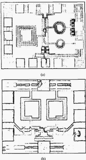
The proposed down-conversion mixer and VCO were implemented in a standard 0. I8-pm CMOS technology. Figure 3 shows the micrographs of the fabricated circuits.
A. Down-Conversion Mixer
In order to demonstrate the ultra-low-voltage operation, a supply voltage of 0.6 V is used for the measurement. The mixer core consumes a dc power of 792 pW. With a 5 . 2 - G k RF frequency and a 5.1-GHz LO frequency, the conversion gain versus LO power is shown in Fig. 4. A maximum conversion gain of 3 d 3 is obtained at a LO power of -2 dBm. The moderate conversion gain of the mixer is mainly due to the limitations on the power consumption and the supply voltage. Good input matching
r - I . k. I
. .
I
I
Fig. 3. The micrograph of (a) down-conversion mixer (b) VCO.
V I , I
-6 -3 0 3 6
LO Power. (dBm)
Fig. 4. The conversion gain of the mixer versus LO power.
h
E
-20?!
g
4 0a
-
3 a I 6 0 I I Pin-ldB liP3I
-80 , -30 -25 -20 -1 5 -1 0 -5 RF Input Power (dBm)Fig. 5. The measured Pi,-lda and IIP3 of the mixer with input frequency spacing of 10 MHz:
is achieved at the RF port with the source degeneration of MN1. An input return loss better than 10 dB is obtained at the RF frequency band.
The linearity of the mixer was characterized by
measuring the P i n - l d B and the IIP3 of the circuit as shown in
Fig. 5 . Based on a two-tone test with an input frequency spacing of 10 MHz, the measured P i n - l d B and IIP3 are -15
and -8 dBm, respectively. The performance of the
proposed mixer is summarized in Table I together with the results Erom the previously published data [4]-[6] for comparison. As indicated in Table I, the mixer presented in this work exhibits the lowest power consumption and
supply voltage €or active mixers while maintaining a
reasonable conversion gain at the 5-GHz frequency band.
6.1 6 h
2
5.99,
3
5.8 5.7 5.6 C al 3 L 5.5!
1
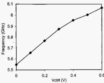
0 0.2 0.4 0.6 Vctrl (V)Fig. 6. The frequency tuning characteristics of the VCO.
M k r l A 1.00 MHr Ref 0 dBm Atten 10 dB -47.13 dB Peak log 18 dB/ 1.11 $2 S3 FC Span 10 MHz Center 5.808 GHz
.
Sweep 4 ms (401 pts) UBW 188 kHz Res BW 180 kH2Fig. 7. The phase noise measurement of the VCO.
B. VCO
The fabricated VCO was tested for ultra-low-power and ultra-low-voltage operation. The VCO core consumes a dc
power 696 pW from a reduced supply voltage of 0.6 V.
Figure 6 shows the frequency tuning characteristics of the VCO. As the controlled voltage sweeps from 0 to 0.6 V, the oscillating frequency varies from 5.55 to 6.05 GHz, exhibiting a frequency tuning range of 8.9%. The phase noise measurement of the VCO is illustrated in Fig. 7. With an output frequency of 5.8 GHz, the measured phase noise is -97 dBc/Hz at 1-MHz offset. The performance of the VCO is summarized in Table 11.
TABLE
r
PERFORMANCE SUMMARY OF THE LOW-POWER AND LO W-VOLTAGE MIXER
1V. CONCLUSION
In this paper, Iow-voltage circuit topologies have been proposed for RF applications. Using a standard 0.IX-pm CMOS process, the RF frontend circuits are designed for wireless communications at 5-GHz frequency band. The
single-balanced mixer employs a folded circuit topology with a current-bleed& technique. The fabricated circuit exhibits a conversion gain of 3 dB with a 5.2-GHz RF
frequency while consuming a dc power of 792 pW from a
supply voltage of 0.6 V. The cross-coupled LC-tank VCO
topology is modified for low-voltage operation by
eliminating the tail transistor. Drawing a dc current of
1.16 mA from a 0.6-V power supply, the VCO has a
frequency tuning range of 8.9% and a phase noise of -97
dBc/Hz at 1-MHz offset. The proposed down-conversion
mixer and ‘the VCO demonstrate the potential of implementing CMOS
RF
circuits for ultra-low-power and ultra-low-voltage applications.ACKNOWLEDGEMENT
This work was supported in part by the National
Science Council under Grant No. 93-2220-E-002-003 and
93-2220-E-002-009. The authors would like to thank National Chip Implementation Center (CIC) for chip fabrication and technical supports.
TABLE I1
PERFORMANCE SUMMARY OF THE LOW-POWER AND LOW-VOLTAGE VCO
REFERENCES
Hooman Darabi, et al., “A 2.4-GHz CMOS transceiver for
bluetooth,” IEEE J. Solid-Stafe Circuits, vol. 36, no.12, pp.2016-2024, Dec. 2001.
Pengfei Zhang, et al., “A 5-GHz direct-conversion CMOS transceiver,” IEEE J. Solid-Stare Circuits, vol. 38, no. 12,
pp. 2232-2238, Dec. 2003.
Iason Vassiliou, et al., “A single-chip digitally calibrated
5.15-5.825GHz 0.18-pm CMOS transceiver for 802. I la wireless LAN,” IEEE J. Solid-State Circuifs, vol. 38, no.
12, pp. 2221-2231, Dec. 2003.
Xuezhen W m g and R. Weber, “A novel low-voltage low-
power 5.8 GHz CMOS down-conversion mixer design,”
Radio and Wireless Conference 2003,pp. 301 - 304,
Aug. 2003.
Chih-Chun Tang, et al., “A 2.4-GHz CMOS down-
conversion doubly balanced mixer with low suppIy
voltage,” ISCAS2001, vol. 4, pp. 794-797, May 2001.
T. Wakimoto, et al.,“ Sub 1 -V 5-GHz-band up- and down-
conversion mixer cores in 0.35-prn CMOS,” VLSI
Circuits Symposium 2000, pp. 98 - 99, June 2000. A. H. Mostafa, M. N. El-Gama1 and R. A. Rafla, “A Sub-
I-V 4-GHz CMOS VCO and a 12.5-GHz oscillator for
low-voltage and high-frequency applications,” Circuits and Systems 11: Analog and Digital Signal Processing, vol. 4 8 , no. 1 0 , pp. 919-926, Oct. 2001.
M. N. EI-Gama], K. H. Lee and T. K. Tsang, “Very low- voltage ( 0 . W ) CMOS receiver frontend for 5GHz F S applications”, Circuits, Devices and Systems. IEE
Proceedings, vol.149, 110.516, pp.355 - 362, Oct.-Dec.
2002.
N. Troedsson and H. Sjoland, “An ultra low voltage 2.4
GHz CMOS VCO,” Radio and Wireless Conference 2002,
pp. 205-208, Aug. 2002.