國 立 交 通 大 學
電子工程學系電子研究所碩士班
碩 士 論 文
應用於超寬頻系統之低功率主動性相位分
離器與混波器之設計
Design Low Power Active Balun and Mixer
for Ultra-Wideband Application
研究生: 徐達道
指導教授: 郭建男 教授
應用於超寬頻系統之低功率主動性相位分離器與混波
器之設計
Design Low Power Active Balun and Mixer for
Ultra-Wideband Application
研 究 生:徐達道 Student: Ta-Tao Hsu
指導教授:郭建男 教授 Advisor: Chien-Nan Kuo
國立交通大學
電子工程學系 電子研究所碩士班
碩士論文
A Thesis
Submitted to Department of Electronics Engineering & Institute of Electronics College of Electrical and Computer Engineering
National Chiao Tung University In Partial Fulfillment of the Requirements
For the Degree of Master
In
Electronics Engineering
June 2006
HsinChu, Taiwan, Republic of China
應用於超寬頻系統之低功率主動性相位分離器與混波器之
設計
學生: 徐達道 指導教授: 郭建男教授
國立交通大學 電子工程學系 電子研究所碩士班
摘要
本篇論文主旨在於利用標準 0.18um CMOS 製程設計適用於超寬頻系統前端 接受器之低功率主動性相位分離器與混波器積體電路,此外並利用新設計的混波 器架構結合低雜訊放大器組成低功率、低電壓窄頻接收器前端電路。2 顆低功率 超寬頻主動性相位分離器、1 顆低功率、低電壓混波器結合主動性相位分離器與 1 顆低功率、低電壓接收器前端電路皆已經由晶片製作而被驗證。 主動性相位分離器方面採用全新的架構,不同於以往利用差動放大器架構 來達成主動性相位分離器的方法,而是利用 NMOS 在上 PMOS 在下的串接方式,避 免電流源的寄生效應,以大幅增加頻寬,且同時利用 Current Reuse 的方法,大 幅降低了功率損耗,根據量測結果可以得到在 Gain Error 小於 2 dB 且 Phase Error 小於 3 度的條件下,可用頻寬高達 8 GHz,而整個電路的功率損耗僅為 1.44 mW 且 Supply Voltage 為 1.2 V,相較於傳統的主動性相位分離器功率損耗約為 12 mW,已大幅節省約 88%。當主動性相位分離器其後接上混波器或其它可調式差動輸入電路時,將造 成主動性相位分離器的輸出負載改變,故根據實際需要改良原本第一顆主動性相
位分離器,將 NMOS 的 Loading 由原本的電阻改為工作在三極體區的 PMOS,利用 改變其 Gate 偏壓 (Vtune) 將其 Rds 改變,使其成為 0~10 GHz 抗製程變異與對 應輸出負載變化的主動性相位分離器,根據模擬結果,在 Gain Error 小於 2 dB 且 Phase Error 小於 3 度的條件下,可用頻寬高達 10 GHz,而整個電路的功率 損耗僅為 1.44 mW 且 Supply Voltage 為 1.2 V,Output Loading 在 25 ~ 200 歐 姆的範圍下均可利用改變 Tunable Resister (Rds)來達成預期的效能,Vtune 每變化 0.1 V, Gain Difference 變化 1 dB 而 Phase Difference 變化 1.5 度。
混波器方面為了降低 Supply Voltage,而將原本的 Gilbert Mixer gm stage 與 switch stage 串接方式改為將 LO 與 RF DC 分流,使每個 MOS 接有足夠的 Vds 跨壓,並且為了在 Low Power 下工作,將 LO 由大訊號改為小訊號的方式,使得 Mixer 一直工作於 subthreshold region,因在工作期間並無 MOS turn off 利用 兩倍的 Conversion Gain 且加上大 RL的方式來達到足夠的 Conversion Gain,利
用此新設計的混波器分別完成了 Low Voltage 1.5 mW 6~10.6-GHz UWB CMOS Mixer With Active Balun 與 Low Voltage 0.86 mW 5~6 GHz Front End。
根據量測結果 Low Voltage 1.5 mW 6~10.6-GHz UWB CMOS Mixer With Active Balun 在功率損耗為 1.56 mW 且 VDD=1.2 V 下提供平坦的 Conversion Gain
為 10 dB ± 1.5 dB from 6 GHz to 10 GHz, NF 約為 15 dB 而 IIP3 約為 3 dBm。 Low Voltage 0.86 mW 5~6 GHz Front End 量測結果則為,在 supply voltage 為 1 V 且功率損耗為 0.86 mW 下,最大的 conversion gain 為 25 dB at 5.3 GHz, 3 dB 頻寬為 1 GHz, NF 約為 12 dB 而 IIP3 大約 -6 dBm。
Design Low Power Active Balun and Mixer for
Ultra-Wideband Application
Student: Ta-Tao Hsu Advisor: Prof. Chien-Nan Kuo
Department of Electronics Engineering & Institute of
Electronics National Chiao-Tung University
ABSTRACT
The aim in this thesis is mainly based on the design of active balun and mixer in the receiver front end of ultra-wideband system using standard 0.18um CMOS process. Also, a low power low voltage narrow band front end is composed of a new mixer and a low noise amplifier. Two low power UWB active baluns, one low power mixer combined with a low power active balun and one low power low voltage front end were verified through 4 individual chips.
In the first chip, an 8 GHz Low Power Ultra-Wideband Active Balun is analyzed and designed. We employ a new topology to design active balun and greatly reduce power consumption and extend the available bandwidth. Measured data show that the bandwidth extends to 8 GHz, gain difference is less than 2 dB, phase difference is less than 3 degree and differential gain has flat gain about -2 dB while consuming 1.5mW.
In the second chip, an ultra wide band low power tunable active balun for process variation compensation is analyzed and designed. A tunable active resister is adopted to improve the first chip. Measured data show that the active balun has a tunable function for process variation compensation is its most important property.
In the third chip, a new design of a low power low voltage mixer is combined with an active balun of the first chip. All transistors in the mixer are biased in the subthreshold region to approach low power application. Use large resisters about 800 Ω as output loading to have high conversion gain and the gain of balun and mixer compensate each other to form a flat gain from 6 to 10 GHz. Measured data show that the flat conversion gain is 9.5 dB ± 1.5 dB from 6 GHz to 10 GHz, NF is about 15 dB and IIP3 is about 3 dBm while consuming 1.5mW.
In the final chip, a 5~6 GHz low power receiver front-end circuit is analyzed and designed. Employ the mixer of the third chip and modify the mixer from double balance to single balance. The single input mixer combines with a single output LNA and all supply voltages are reduced to 1 V to form the 5 ~ 6 GHz 1V low power receiver front-end circuit. Measured data show that the max conversion gain is 25 dB at 5 GHz, 3 dB bandwidth is about 1 GHz, NF is about 10 dB and IIP3 is about -6 dBm while consuming 0.8mW.
誌謝
能夠完成論文主要要感謝我的指導教授郭建男教授,老師這兩年來給我很多 指導與鼓勵,使我在碩士生涯的期間能有幸踏入射頻的領域,並且能有效率的成 長,更重要的是了解到做學問應有的態度與方法,在此向老師表達我內心最深的 敬意與感謝。 另外要感謝陳巍仁和鄭裕庭教授兩年來在計劃的會議上分享研究成果與想 法,得以讓我有學到更多更廣的機會。再來就是博班學長昶綜,鈞琳和明清給我 很多意見與指教讓我受益非淺在這邊表達感謝;碩一時幸虧有志修,英瑞,維嘉, 仰鵑和坤宏學長姐的幫助才能讓我儘快的投入研究,還有我的同學子倫和岱原與 學弟妹清揚,宗男,俊興和燕霖因為有你們陪伴我碩士的生活,使我在成長的路 上不曾感到孤單,一起研究,一起討論,就像一個大家庭。還要感謝國家晶片中 心(CIC)在電路實做和晶片量測上所提供的協助。 最後,要感謝我的父母給我的栽培與鼓勵,及所有家人的支持,還有我的女 朋友佳真陪在我的身邊分享我的喜怒哀樂,還要感謝的人很多,在此一併謝過。 徐達道 九十五年 六月CONTENTS
ABSTRACT (CHINESE) …...i
ABSTRACT (ENGLISH) ...iii
ACKNOWLEDGEMENT ………..………...v
CONTENTS……...vi
TABLE CAPTIONS...x
FIGURE CAPTIONS...xi
Chapter 1
Introduction………..………...1
1.1 System Overview...………...1
1.2 Motivation...…………...………...2
1.3 Thesis Organization………3
Chapter 2 The Fundamental Designs of Front-End...4
2.1 Front-End Architecture…………...4
2.2.1 Low Noise Amplifier Architecture Analysis…..………….6
2.2.2 Optimizations of Low Noise Amplifier Design Flow.……9
2.3 Design Basic in Active Baluns……….………...11
2.3.1 Differential Amplifier with a Series LCR Feedback as
Active Balun Analysis ………..…....…………...15
2.4 Down-Conversion Mixer Basic…………...………...17
2.4.1 Conversion Gain…..…………...19
2.4.2 Switching Stage………..………..…..……19
2.4.3 Mixer Noise…...…..…...20
2.4.4 Port-to-Port Isolation………..………..…..……21
Chapter 3 Low Power Ultra-Wideband Active
Balun………...22
3.1 Introduction………..…………...22
3.2 Low Power Ultra-Wideband Active Balun…..………….22
3.2.1 8 GHz Low Power Ultra-Wideband Active Balun……….22
3.2.2 Microphotograph of Chip...27
3.2.3 Simulation and Measurement results and Discussion……28
3.3.1 Design on 0~10 GHz Ultra Wide-Band Low Power Tunable
Active Balun for Process Variation Compensation...38
3.3.2 Microphotograph of Chip...44
3.3.3 Simulation and Measurement results and Discussion…...45
Chapter4 Low Power Ultra-Wideband
CMOS Mixer
with Active Balun..
………..51
4.1 Introduction………...51
4.2 Low Voltage 0.2-mW CMOS Mixer
….
………51
4.3 Low Voltage 1.5-mW 6~10.6-GHz Ultra-Wideband CMOS
Mixer With Active Balun ……….57
4.3.1 Microphotograph of Chip……….59
4.3.2 Simulation and Measurement results and Discussion…..60
Chapter5 Low-Power Front-End Circuit...……65
5.1 Introduction……….………....65
5.2 Low Voltage 0.2-mW 5 ~ 6 GHz Front-End ……..……66
5.2.1 Low Noise Amplifier…..…………..………...67
5.2.2 Low Voltage 0.2-mW CMOS Mixer.………..…….68
5.2.3 Microphotograph of Chip………..………...70
5.2.4 Simulation and Measurement results and Discussion...71
Chapter6 Conclusion………...………76
Chapter7 Future Work…….…………...………78
REFERENCES..………...79
TABLE CAPTIONS
TABLE 3.1 Summary of measured performance and comparison to other active balun………..………..35
TABLE 3.2 Summary of measured performance and comparison to the simulated
performance………..……...50 TABLE 4.1 Performance summary for mixer..………...64
TABLE 4.2 Performance summary for the mixer with the active balun………..64
FIGURE CAPTIONS
Fig 1.1 Multi-band spectrum allocation………...2
Fig. 2.1 Front-End………...5
Fig. 2.2 Common-source input stage with inductive source degeneration……….5
Fig. 2.3 Equivalent noise model of Figure 2.2………..…………...………..7
Fig.2.4 the single FET circuits as active balun………....12
Fig. 2.5 common-gate common-source (CGCS) circuit as active balun…………13
Fig. 2.6 Differential amplifier as active balun………14
Fig. 2.7 Differential amplifier with LCR feedback as active balun………15
Fig. 2.8 Simplified CMOS Gilbert Cell mixer………18
Fig. 3.1 Front-End……….…………..22
Fig. 3.2 Modify the differential amplifier………...23
Fig. 3.3. Schematic of the proposed balun circuit.………..………..24
Fig. 3.4. Small-signal equivalent circuit model of the proposed balun circuit..……25
Fig. 3.5. Micrograph of the fabricated active balun………...27
Fig. 3.6. Measured data and simulation of gain difference…………..………..31
Fig. 3.7. Measured data and simulation of phase difference…….………....31
Fig. 3.8. Measured IIP3 of the active balun………...32
Fig. 3.9. Measured NF………..……….32
Fig. 3.11. Measured Difference Gain………..………33
Fig. 3.12. Simulated Differential Gain without R1………...……..…34
Fig. 3.13. Simulated NF without R1………...………..….…….34
Fig. 3.14. Proposed active balun combined with the next stage………..…...37
Fig. 3.15. The simulated gain difference and phase difference with difference RL………..37
Fig. 3.16. The proposed tunable active balun………..…………...38
Fig. 3.17. PMOS I_V curve……….……….39
Fig. 3.18. The equivalent model of the PMOS M1on the triode region………...39
Fig. 3.19. Small-signal equivalent circuit model of the proposed tunable balun circuit …40 Fig. 3.20. Phase difference vs. Vtune……….………...43
Fig. 3.21. Gain difference vs. Vtune……….43
Fig. 3.22. Micrograph of the fabricated tunable active balun.………..44
Fig. 3.23. Measure I_V curve of the active resister. ……….……...46
Fig. 3.24. Measured I_V curve of the active resister M1..…………..……….….46
Fig. 3.25. The measured I_V curve of the active resister compared with the simulated IV curve under TT & SS corner test………47
Fig. 3.26. DC voltage at node A and node B……….48
Fig. 3.27. Measured S11 and Measured S12….………..……..49
Fig. 4.1 Schematic of the proposed mixer circuit…..………...53
Fig. 4.2 The real current (DC+AC) when the voltage swing of LO at the source of M5~M8 is about 0 dBm……….…55
Fig. 4.2.1 The voltage transfer characteristic of a CMOS amplifier.………56
Fig. 4.3 Schematic of the proposed mixer with the proposed active balun circuit………...57
Fig. 4.4 Illustration of broadband gain flatness, (a) conversion gain for the active balun, (b)conversion gain for the mixer, and (c) conversion gain for the mixer combined with the balun.………..………..58
Fig. 4.5 Micrograph of the fabricated mixer with the active balun………..…...59
Fig 4.6 Gain Difference & Phase Difference at Node A and B in Fig 4.3……..61
Fig 4.7 Measurement diagram including unit gain output buffer………...61
Fig. 4.8 Measured S11………62
Fig. 4.9 Measured Conversion Gain………62
Fig. 4.10 Measured IIP3………63
Fig. 4.11 Measured NF..……….…..….63
Fig. 5.1 The block diagram of the front-end circuit………..…..65
Fig. 5.2 The schematic of the front-end circuit………...……66
Fig. 5.3 The schematic of low noise amplifier………67
Fig. 5.5 Micrograph of the fabricated front end………70
Fig. 5.5 Measurement diagram including unit gain output buffer………72
Fig. 5.6 Measured S11………..72
Fig. 5.7 Measured Conversion Gain…….………73
Fig. 5.8 Measured IIP3……….73
Chapter 1
Introduction
1.1 System Overview
The Multi-band OFDM Alliance (MBOA) standard for UWB communications
draws heavily upon prior research in wireless local area network (WLAN) systems.
The UWB system is an emerging high-speed and low-power wireless communication
approved by Federal Communication Commission (FCC). The multi-band UWB has
greater flexibility in coexisting with other international wireless systems and future
government regulators, and could avoid transmitting in already occupied bands. In a
manner similar to IEEE 802.11 a/g, MOBA partitions the spectrum from 3 to 10 GHz
into 825-MHz bands and employs OFDM in each band to transmit data rates as high
as 480 Mb/s. Fig. 1.1 shows the structure of MOBA bands and the channelization
within each band. The 13 bands span the range of 3.1 to 10.6 GHz. The frequency
operation for Mode 1 device allocates in 3.1GHz to 5GHz and the one for Mode 2
1.2 Motivation
The balun circuits always play the critical component in RF system if they are necessary. For example, it is often between the single output LNA and the double balance mixer. Usually, the passive balun is adopted because of no power consumption. But the large physical size of the passive balun is hard to cost down. So, to design an active balun with limited power consumption even has flat gain is a critical challenge for design. How to do that is one of the main objects of this thesis
Typical, the first stage of the receiver is a low noise amplifier (LNA), which provides high gain and low noise to suppress the overall system’s noise performance. After balun, the mixer transforms the radio-frequency (RF) signal into base-band directly and needs high linearity to avoid the distortion of the signal. Because there is a LNA to suppress the overall system’s noise performance, the noise performance of the mixer is not the most important design target. So, how to decrease the power consumption as small as possible and this mixer has an acceptable linearity at the same time is the other main object of this thesis.
GROUP A GROUP B GROUP C GROUP D
Band #1 Band #2 Band #3 Band #4 Band #5 Band #6 Band #7 Band #8 Band #9 Band #10 Band #11 Band #12 Band #13 3432 MHz 3960 MHz 4488 MHz 5016 MHz 5808 MHz 6336 MHz 6864 MHz 7392 MHz 7920 MHz 8448 MHz 8976 MHz 9504 MHz 10032 MHz
f
Fig 1.1 Multi-band spectrum allocation1.3 Thesis Organization
In the chapter 2, the fundamental designs of front-end will be introduced.
In the chapter 3, the 8 GHz low power ultra-wideband active balun is presented in
section 3.2. And the modified active balun, 0~10 GHz ultra wide-band low power
tunable active balun for loading variation and process variation compensation is
discussed in section 3.3.
In the chapter 4, the low voltage 0.2-mW CMOS mixer is presented in section 4.2.
And low voltage 2-mW 6~10.6-GHz ultra-wideband CMOS mixer with active balun
is introduced in section 4.3.
In the chapter 5, to discuss the low-power front-end circuit design. In the last chapter, the work is summarized and concluded.
Chapter 2
The Fundamental Designs of Front-End
The fundamental designs of the front-end architecture will be presented in this chapter. Section 2.1 gives the front-end architecture first. The design basic in LNA will be introduced in the section 2.3. The popular active balun at high frequency is discussed in section 2.4, and the end of this chapter will introduces the basic design of the mixer.
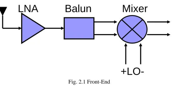
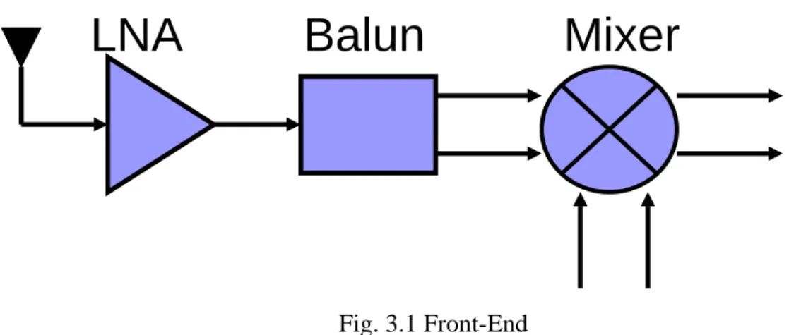
2.1 Front-End Architecture
In receiver architecture, input signals are translated into much lower frequencies by down-conversion mixer, and the active balun generates the differential output signals for double balance mixer from the signal input signal. Generally, the low noise amplifier is in the first stage for reducing noise from the active balun and the down-conversion mixer. A simple front-end architecture is shown in Fig. 2.1. I adopt the homodyne receiver due to the following reasons:
(1) The problem of image is removed due to ωIF= 0. Therefore no image filter is required, and the LNA need not drive a 50-Ω load.
(2) It is attractive for monolithic integration because this architecture needs less external components.
For the above reasons, this architecture is suitable for low-power and signal-chip design.
2.2 Low Noise Amplifier Basic
Low noise amplifier is the first gain stage in the receiver path so its noise figure directly adds to that of the system. Therefore, there are several common goals in the design of LNA. These include minimizing noise figure of the amplifier, providing enough gain with sufficient linearity and provide a stable 50Ω input impedance to terminate an unknown length of transmission line which delivers signal from antenna to the amplifier. Among LNA architectures, inductive source degeneration is the most popular method since it achieve noise and power matching simultaneously, as shown in Fig. 2.2. The following analysis is based on this architecture.
Balun
Mixer
LNA
+LO-Fig. 2.1 Front-End
L
gZ
inM
1L
s2.2.1 Low Noise Amplifier Architecture Analysis
In Fig. 3.1, the input impedance can be expressed ass gs m gs s g in L C g sC L L s Z = ( + )+ 1 +( ) s T s gs m
L
L
C
g
ω
≈
=
(
)
at gs s g L C L ) ( 1 0 + = =ω
ω
As shown in (2-1), the input impedance is equal to the multiplication of cutoff frequency of the device and source inductor at resonant frequency. Therefore it can be set to 50Ω for input matching while resonant frequency is designed to be equal to the operating frequency.
According to prior introduction, the equivalent noise model of common-source LNA with inductive source degeneration can be expressed as Fig. 2.3, where Rl is the
parasitic resistance of the inductor, Rg is the gate resistance of the device. Note that
the overlap capacitance Cgd has also been neglected in the interest of simplicity. Then the noise figure can be obtained by computing the total output noise power and output noise power due to input source. To find the output noise, we first evaluate the transconductance of the input stage. With the output current proportional to the voltage on Cgs and noting that the input circuit takes the form of series-resonant network, the transconductance at the resonant frequency can be expressed as
s T s T s gs m in m m
R
L
R
C
g
Q
g
G
0 0(
)
2
ω
ω
ω
ω
+
=
=
=
(2-2) (2-1)Qin is the effective Q of the amplifier input circuit. So the output noise power density due to the source can be expressed as
2
)
1
(
4
)
(
2 0 2 . 2 0 , s s T s T eff m Rs Rs aR
L
R
kT
G
S
S
ω
ω
ω
ω
+
=
=
In the similar way, the output noise power density due to Rg and Rl is
2 2 2 0 2 0 , ,
)
1
(
)
(
4
)
(
s s T s T l g Rl Rg aR
L
R
R
R
kT
S
ω
ω
ω
ω
+
+
=
Furthermore, channel current noise of the device is the dominant noise contributor, and its noise power density associated with the correlated portion of the gate noise can be expressed as
2
)
1
(
4
)
(
0 , , s s T do i i aR
L
g
kT
S
ngc ndω
γκ
ω
+
=
Where γ is the coefficient of channel thermal noise, α= gm / gdo and
v
s 2R
sL
gv
Rl 2R
lv
Rg 2R
gi
2ngci
2 nguC
gs+
v
gs-
g
mv
gsi
2ndL
si
2outFig. 2.3 Equivalent noise model of Figure 2.2
(2-3)
(2-4)
2 2 2 2
5
1
5
⎥
⎥
⎦
⎤
⎢
⎢
⎣
⎡
+
+
=
γ
δα
γ
δα
κ
c
c
Q
L gs s LC
R
Q
01
ω
=
The last noise term is the contribution of the uncorrelated portion of the gate noise, and its output noise power density can be express as
2 0 ,
)
1
(
4
)
(
s s T do i aR
L
g
kT
S
nguω
γξ
ω
+
=
where)
1
)(
1
(
5
2 2 2 LQ
c
+
−
=
γ
δα
ξ
According to (2-3),(2-4),(2-5) and (2-8), the noise figure at the resonant frequency can be expressed as
)
(
1
0 T L s g s lQ
R
R
R
R
F
ω
ω
α
γχ
+
+
+
=
where)
1
(
5
5
2
1
2 2 2 L LQ
Q
c
+
+
+
=
γ
δα
γ
δα
χ
From (2-11), we observe that χ includes the terms which are constant, proportional to QL, and proportional to QL2. It follows that (2-11) will contain terms which are proportional to QL as well as inversely proportional to QL. A minimum noise figure, therefore, exits for a particular QL.
(2-6) (2-7) (2-8) (2-9) (2-10) (2-11)
2.2.2 Optimizations of Low Noise Amplifier Design Flow
The analysis of the previous section can now be drawn upon in designing the LNA. In order to pick the appropriate device size and bias point to optimize noise performance given specific objectives for gain and power dissipation, a simple second-order model of the MOSFET transconductance can be employed which accounts for high-field effects in short channel devices. Assuming that the drain current, Id, has the form
ρ
ρ
+
=
−
+
−
=
1
1
)
(
2 sat sat ox T gs sat T gs sat ox DSWC
v
LE
V
V
LE
V
V
v
WC
I
where sat T gsLE
V
V
−
≡
ρ
. And the (2-7) can be replace asWL
Q
R
C
R
WLC
Q
L s ox s ox L 0 02
3
2
3
ω
ω
⇒
=
=
The power consumption of the LNA, therefore, can be expressed as
ρ
ρ
ω
+
=
=
1
1
2
3
2 0 sat sat s L DD DS DD Dv
E
R
Q
V
I
V
P
The noise figure can be expressed in terms of PD and Vgs. Two parameters linked to power dissipation need to be accounted for.
where s sat sat DD
R
E
v
V
P
0 02
3
ω
=
. (2-12) (2-13) (2-14) (2-15) (2-16))
,
(
1
1
2
3
)
(
2 2 0 2 0 1 D gs D s D sat sat DD L gs gs m TP
V
f
P
P
R
P
E
v
V
Q
V
f
C
g
=
+
=
+
=
=
≈
ρ
ρ
ρ
ρ
ω
ω
The noise figure of the LNA, therefore, can be expressed as
)
,
(
))
1
(
5
5
2
1
)(
(
1
2 2 2 0 D gs L L T L s g s lc
Q
Q
f
V
P
Q
R
R
R
R
F
=
+
+
+
+
+
+
=
γ
δα
γ
δα
ω
ω
α
γ
In general, there are two approaches to optimize noise figure. The first approach assumes a fixed transconductance, Gm. The second approach assumes fixed power consumption.
(1) Fixed Gm optimization: To fix the value of the transconductance, G m ,we need only assign a constant value to ρ. Onceρ is determined, the optimization of the noise figure can be obtained by (2-17):
) , ( 0 ) , ( . .
.opt Lopt gs Dopt D fixedVgs D D gs P V f F Q P P P V f = ⇒ ⇒ ⇒ = ∂ ∂
From (2-13), we can obtain the optimal width to get the minimal noise figure for a given Gm under the assumption of matched input impedance. In this approach, the designer can achieve high gain and low noise performance by selecting the desired transconductance, but its disadvantage is that we must sacrifice the power consumption to achieve minimum noise figure.
(2) Fixed PD optimization: An alternative method of optimization fixes the power dissipation and adjusts device size and bias point to minimize the noise figure. Once PD is determined, the optimization of the noise figure can be obtained by (2-19): ) , ( 0 ) , ( . .
.opt Lopt gsopt D gs fixedPD gs D gs P V f F Q V V P V f = ⇒ ⇒ ⇒ = ∂ ∂
Then the optimum device size can be obtained to get the best noise performance for fixed power dissipation. In this approach, the designer can specify the power dissipation and find the optimal noise performance, but its disadvantage is that the
(2-17)
(2-18)
transconductance is held up by the optimal noise condition.
2.3 Design Basic in Active Baluns
Differential baluns (or phase splitters) are basic cells required in microwave
components such as balanced mixers, multipliers, and phase shifters. An ideal
differential phase splitter will generate a pair of differential signals which have
balanced amplitude and phase (0 dB gain difference and 180°) from a single input.
In RFIC there are passive and active differential phase splitter or baluns. LC
networks can be used for narrow-band passive baluns; microstriplines can be used for
wide-band passive baluns. However, the spiral inductors, MIM capacitors, and
microstriplines in RFIC are too expensive due to their larger physical size at lower
microwave frequencies. There are three categories of active balun circuits normally
employed in lower microwave frequencies for wireless communications: single FET
circuits, common-gate common-source circuits and differential amplifier circuits.
Fig. 2.4 shows the single FET circuits as active balun. It is probably the
simplest. At low frequency the small signal circuit of this active balun can ignores all
parasitic effect. Under this condition, this circuit can produces a pair of differential
output signals at the drain and source of the FET respectively. At higher frequency
range, this circuit is limited by imbalances caused by the imbalances caused by
1dB and 176° at 950 MHz. To make it applicable at higher frequency, a sophisticated
imbalance cancellation technique was used to improve the performance beyond 1
GHz. It had 1 dB amplitude difference and 172° pahse difference (-8° unbalance)
from 700 MHz to 1.7 GHz. However, the tradeoff was the increase of circuit
complexity, die area, and dc current. For accurate results beyond 2 GHz, the
application of the signal FET circuit is questionable.
Fig.2.4 the single FET circuits as active balun
Vdd
RFin
Vo1
Vo2
R
LR
LR
INFig.2.5 shows the common-gate common-source (CGCS) circuit as active balun.
The common-gate common-source (CGCS) circuit provides equal amplitudes split
with 180° phase difference. In this configuration, the ac coupling capacitance and
bypass capacitance need to be adjusted separately to optimize at a specific frequency
to achieve balanced differential signals. Therefore, this configuration is only good for
narrow-band application are around 0.5-2 dB and 177-189° due to the process
variation and asymmetric signal path.
The differential amplifier circuit is shown in Fig. 2.6. It is very popular to apply
the differential amplifier as active balun at high frequency. Ideally, this circuit will
provide equal amplitude (or gain) and 180° phase difference. However, due to the
finite impedance at node “A” caused by strong parasitic at high frequency, the gain Fig. 2.5 common-gate common-source (CGCS) circuit as active balun
V
DDRFin
Vo
1
Vo
2
R
L1V
DDR
L2and phase balance are poor.
An active device is often used as the current source. However, besides the finite
impedance at node “A”, the voltage drop across the drain and source make it difficult
to realize in low power supply circuit as required by the portable wireless applications
(Vdd < 3V or even < 2V). According to simulation result, the output amplitude
difference can be 2 dB or the phase difference can be poorer than 174°, within
frequency range from dc to 6 GHz.
The active current source was replaced by an inductor to increase the
impedance of S1 at high frequencies. When an ideal inductor with unlimited value (dc
through and ac block) is used as the current source, excellent results can be obtained.
A
Vin
V
DDVo1
Vo2
However, this extra large ideal inductor is not viable to be realized on-chip due to
large physical size. This circuit obtained 1dB gain difference and 175 ° phase
difference at the specific frequency, at other frequencies, the gain and phase balance
are poor. Therefore, it is only applicable for narrow-band applications.
2.3.1 Differential Amplifier with a Series LCR Feedback as
Active Balun Analysis
Fig. 2.7 shows the differential amplifier with LCR feedback as active balun. It
is most popular to apply this circuit as an active balun at high frequency. The
feedback circuit consists of twisters R2 and RF, an inductor LF, and a capacitor CF. Fig. 2.7 Differential amplifier with LCR feedback as active balun
CF
LF
RF
Vin
VDD
Vo1
Vo2
R2
R1
M1
M2
This feedback circuit will helpo res to reduce the Vo1 power and increase the Vo2
power. The resister R2 plays two roles: it keeps dc bias of M2 the same as T1, at the
same time it senses the signal fed back from the drain of M1. CF provides a dc blocking function so that the feedback circuit will not shift dc bias of M2. At the
application specific frequency ω, if CF and LF values are chosen in such a way that
they follow the equation of
the phase delay from the drain of M1 to the gate of M2 is zero. This is because that
the series LC circuit gives a zero reactance AC equivalent circuit will reduce to RF, R2 and z2, where z2 is M2’s gate input impedance at ω. AC signals on the gate of M2
(vG2) and on the drain of M1 (vD1) have the following relationship:
From (2-2), vG2 can be changed by adjusting RF and R2.
The amplitude tuning of the phase splitter will be taken care of by the ratio of
RF and R2. The phase unbalance can be adjusted by proper choice of reactance of the feedback circuit. The reactance XF is given as
.
XF can be positive (inductive), zero (resistive), or negative (capacitive) by adjusting LF and CF values at the application frequency Ω. Thus, the phase unbalance at output
2
1
ω
=
•
F FC
L
(2-20) 2 2 2 2 2 2//
//
z
R
R
z
R
v
v
F D G=
•
+
(2-21) (2-22) F F F C L Xω
ω
− 1 =ports can be effectively cancelled. From (2-22), it is seen that the phase tuning can be
done in a linear mode by changing LF and keeping CF constant since XF LF, or in nonlinear mode by changing CF and keeping LF constant, or by changing both. The Q factor is not important in this design because the lossy part of the inductor can be
treated as part of RF in the feedback circuit. In RFIC design, the actual choice of LF and CF depends on the consideration of area consumption, phase tuning sensitivity, and process tolerances.
But like the conventional differential amplifier as active balun, the
differential amplifier with RLC feedback as active balun needs twice DC current
paths. It consumes twice DC power consumptions. High power consumption limits
the value of this circuit. And RLC feedback is frequency depend to limit the
bandwidth of this active balun.
2.5 Down-Conversion Mixer Basic
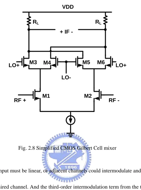
The purpose of the mixer is to convert a signal from one frequency to another. In a receiver, this conversion is from radio frequency to intermediate frequency or zero-IF. Mixing requires a circuit with a nonlinear transfer function, since nonlinearity is fundamentally necessary to generate new frequencies. Fig. 2.8 shows a simplified CMOS Gillbert cell mixer, which is composed of transconductance stage and switching stage.
The RF input must be linear, or adjacent channels could intermodulate and interfere
with the desired channel. And the third-order intermodulation term from the two other
signals will be directly on the top of the desired signal. The LO input need not be
linear, since the LO is clean and of known amplitude. In fact, the LO input is usually
designed to switch the upper quad so that for half the cycle M3 and M6 are on and
taking all current to output loading. For the other half of the LO cycle, M3 and M6 are
off and M4 and M5 are on. This stage will be, therefore, like switch to mixing RF
signal to IF signal. RL + IF -M1 M2 RF + M3 M4 M5 M6 LO+ VDD LO-LO+ RL RF
2.5.1 Conversion Gain
The gain of mixers must be carefully defined to avoid confusion. The voltage conversion gain of a mixer is defined as the ratio of the rms voltage of the IF signal and rms voltage of the RF signal. Note that the frequencies of these two signals are different. The power conversion gain of a mixer is defined as the IF power delivered to the load divided by the available RF power from the source. If the impedances are both matched to 50Ω , then the voltage conversion gain and power conversion gain of the mixer are equal when they are expressed in decibels.
Now, we assume that M3-M6 work like an ideal switch, and the conversion transconductance of the mixer can be expressed as
m c
g
G
π
2
=
where gm is the transconductance of M1 and M2, and 2/π is produced by switching stage.
2.5.2 Switching Stage
For small LO amplitude, the amplitude of the output depends on the amplitude of the LO signal. Thus, gain is larger for larger LO amplitude. For large LO signals, the upper quad switches and no further increase occur. Thus, at this point, there is no longer any sensitivity to LO amplitude. Besides, if upper quad transistors are alternately switched between completely off and fully on, the noise will be minimized. Since upper transistor contributes no noise when it is fully off, and when fully on, the upper transistor behaves like a cascade transistor which does not contribute significantly to noise.
The large LO signal is required to let upper quad transistors achieve complete switching. But if the LO voltage is made too large, a lot of current has to be moved
into and out of the transistors during transitions. This can lead to spikes in the signals and can actually reduce the switching speed and cause an increase in LO feed-through. Thus, too large a signal can be just as bad as too small a signal.
2.5.3 Mixer Noise
Noise figure for a mixer is defined as
In general, the noise figure of the mixer is divided to two categories, single-sideband (SSB) noise figure and double-sideband (DSB) noise figure. The difference between the two definition is the value of the denominator in (2-24). In the case of SSB noise figure, only the noise at the output frequency due to the source that originated at the RF frequency is considered, and it is usually used in heterodyne systems. In the case of DSB noise figure, all the noise at the output frequency due to the source is considered (noise of the source at input and image frequencies), and it is usually used in homodyne system.
Because of the added complexity and the presence of noise that is frequency translated, mixers tend to be much noisier than LNAs. In generally, mixers have three frequency bands where noise is important:
(1) Noise already presents at the IF: The transistors and resistors in the circuit will generate noise at the IF. Some of this noise will make it to the output and corrupt the signal.
(2) Noise at the RF and image frequency: The noise presents at the RF and image frequency will be mixed down to the IF.
(3) Noise at multiples of the LO frequencies: Any noise that is near a multiple of the LO frequency can also be mixed down to the IF, just like the noise at the RF. noise factor = total output noise power at the IF
Besides, the flicker noise will become more important in the homodyne receiver. In the design of the direct down-conversion mixer, how to reduce the flicker noise of upper quad transistors is the important thing. This noise can be reduced by increasing the device size for a given gm.
2.5.4 Port-to-Port Isolation
The isolation between each two ports of a mixer is critical. The LO-RF feed-through results in LO leakage to the LNA and eventually the antenna, whereas the RF-LO feed-through allows strong interferers in the RF path to interact with the local oscillator driving the mixer. The LO-IF feed-through is important because if substantial LO signal exists at the IF output even after low-pass filtering, then the following stage may be desensitized. Fortunately, this feed-through can be reduced largely be used the double-balanced architecture. Finally, the RF-IF isolation determines what fraction of the signal in the RF path directly appears in the IF, a critical issue with respect to the even-order distortion problem in homodyne receivers. The required isolation levels greatly depend on the environment in which the mixer is employed. If the isolation provided by the mixer is inadequate, the preceding or following circuits may be modified to remedy the problem.
Chapter 3
Low Power Ultra-Wideband Active Balun
3.1 Introduction
New low-power CMOS active baluns are designed for ultra-wideband applications, using a pair of common-source NMOS and common-gate PMOS transistors.
This chapter will be divided into two sections. Section 3.2 addresses the new architecture of 8 GHz low power ultra-wideband active balun. Section 3.3 delineates the improved low power ultra-wideband active balun with tunable ability for process variation.
3.2 Low Power Ultra-Wideband Active Balun
3.2.1 8 GHz Low Power Ultra-Wideband Active Balun
Balun circuits are the critical block required in RF and microwave circuits
whereas signal in a balanced format is necessary. An ideal differential balun generate a
Balun
Mixer
LNA
pair of differential output signals of balanced amplitudes and phases (0 dB gain
difference and 180° phase difference) from a single input. The proposed balun is
designed for the front-end application in Fig. 3.1. For ultra wideband, low power and
small area, active balun with limited power consumption is a better choice.
Like mentioned, it is very popular to apply the configuration of a differential
amplifier as active balun at high frequency. But infinite impedance at the current source
limits the bandwidth. And two DC branches need twice DC power consumption. Higher
power consumption limits the value of this kind of active balun, too. I use a PMOS to
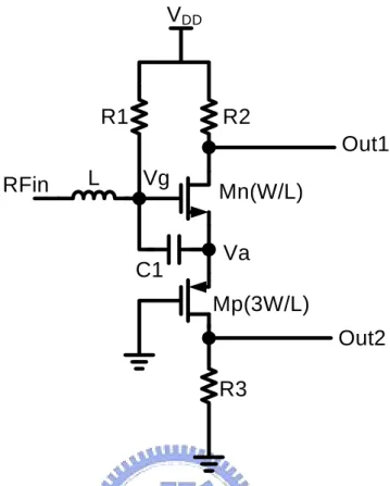
replace a NMOS (M2) in Fig. 3.2., and apply the folded topology . The NMOS Mn and
PMOS Mp both connect at the source ports.
CP RIN Vin M1 M2 VDD RL RL CP RO RO Vo1 Vo2 Zs X Fig. 3.2
24
Fig. 3.3. shows the schematic of the proposed balun circuit, which consists of an
NMOS and a PMOS pair. The two transistors, connected both at the source ports, are
configured in a manner that the NMOS is as common-source, while the PMOS as
common-gate. Reused DC biasing current greatly reduces power consumption. Another
viewpoint of this circuit reveals that the differential amplifier can be considered as a
folded topology of this new balun. The common-source node at Va corresponds to the
current-source node in a differential amplifier. Without using a current source, this
proposed balun needs no feedback compensation for gain and phase imbalance. The
gate ports are directly DC-connected to VDD and the ground, respectively. The resistors
L VDD R1 R2 R3 Mn(W/L) Mp(3W/L) C1 RFin Out1 Out2 Vg Va
R2 and R3 provide DC biasing and output loading. The values must be carefully chosen
to sustain proper biasing of the transistor pair in the saturation condition. Actually the
biasing current shall be small. As such, the Va is biased at the DC voltage around VDD/2.
The impedance matching components, R1 and L, are for measurement purpose. In a
fully integrated system they might be unused when combined with a previous stage.
This proposed balun circuit is advantageous in less circuit complexity, die area, and dc
current.
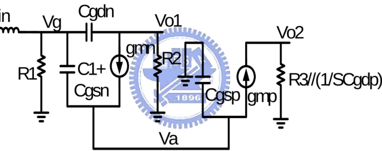
The small-signal equivalent circuit is as shown in Fig. 3.4. Critical to affect
output imbalance, the gate-drain parasitic capacitance, Cgd, shall be included in the
analysis. Derived from the core circuit, the common-source voltage, va, is related to the
gate voltage, vg, as
Vin
R1
Cgdn
C1+
Cgsn
gmn
R2
R3//(1/SCgdp)
Cgsp gmp
Vo1
Vo2
Vg
Va
If the voltage va is one half of the gate voltage vg, two outputs can reach a well-balanced
condition. This leads to the requirement of gmn = gmp and C1+Cgsn = Cgsp. To do so, the
PMOS size is chosen as three times of the NMOS size. An external capacitor, C1, is also
added for the latter requirement. Under these conditions, the voltage ratio of the two
outputs is given by 3 3 2 2 2 1
5
.
0
1
1
)
5
.
0
(
R
g
R
sC
R
sC
sC
g
R
v
v
m gdp gdn gdn m o o⋅
+
+
−
−
=
. (3-2)As can be seen, the impedance matching components affect no gain and phase
imbalance. A balanced output demands vo1 = -vo2. If biasing current is large, then
gdn m C
g >>ω and the condition is fulfilled. In low-power cases, the condition can be fulfilled if the values of R2 and R3 follow these equations,
) ( 2 3 gdn gdp m gdn C C g C R − = , and m gdp gdn
g
C
C
R
R
2 3 22
1
1
ω
+
=
. (3-3) As gm CgdnCgdp 2 2ω>> in the frequency range of interest, the choice of R2 an R3
holds over a broad frequency range. It concludes that the effect on imbalance from the
transistor parasitic is less than that from the compensation feedback and the current
source parasitic. gsp mp gsn mn gsn mn g a
sC
g
C
C
s
g
sC
g
v
v
+
+
+
+
+
=
)
(
1 (3-1)3.2.2 Microphotograph of Chip
A balun circuit was designed in a standard 0.18um CMOS technology. Fig. 3.5.
shows the micrograph of the fabricated circuit. The total chip area is 0.57mm by
0.68mm including bonding pads for on-wafer probing measurements. The area of the
core circuit could be much reduced in a fully integrated circuit. The RF input and output
ports are placed on the opposite sides of the chip to improve the isolation.
Vdd
RFin
gnd
(Out 1)
(Out 2)
G
G
G
S
S
3.2.3 Simulation and Measurement results and Discussion
The load impedance at each output port is the same as the source of 50-Ω. As such, the circuit presents an impedance transformation ratio of 1:2. Specified for
ultra-wideband application, the design is optimized at the frequency of 8-GHz for
minimum phase error and gain imbalance based on Eq. (3-3). The ideal design gives
gain and phase imbalance of ±1dB and ±1.5°, respectively, up to 11-GHz. Post-layout
simulation shows that the circuit achieves imbalance of 2dB and 3° up to 8-GHz. This
circuit could operate under supply voltage variation from 1.2V to 1.5V with reasonable
balanced outputs. It consumes a power level of only 1.44mW, much less than those of
previous work.
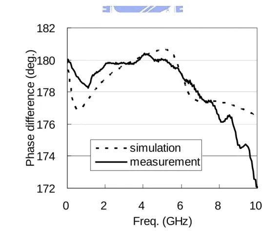
The measurement results of the gain difference and the phase difference are
shown in Fig. 3.6. and Fig. 3.7. It shows good agreement with post-layout simulations,
except at frequencies higher than 6-GHz. The discrepancy of phase difference arises
from measurements conducted by two-port on-wafer probing tests. Although probe
parasitic are well calibrated for the two ports under test, the third port is terminated into
an un-calibrated probe. The unexpected parasitic greatly affects measurements accuracy,
especially for phase imbalance. It is found that by adding a parasitic inductance of 50fH
at the third port output, simulation data approaches to measurement data. The issue
As to the discrepancy of gain difference, it is due to the unaccounted parasitic at
the gate-port of the PMOS. It turns out the gain balance is quite sensitive to an inductive
parasitic at this location.
The measured IIP3 and noise figure at the OUT1 port are shown in Fig. 3.8 and
Fig. 3.9, respectively. The OUT2 port is terminated with a 50Ω resister. The circuit
does give good linearity performance over the entire frequency range. Note that the
noise performance is degraded by the matching resistor R1. This could be improved in a
fully integrated environment without R1. Later Fig 3.13 will show the difference of NF
between having R1 and without R1.
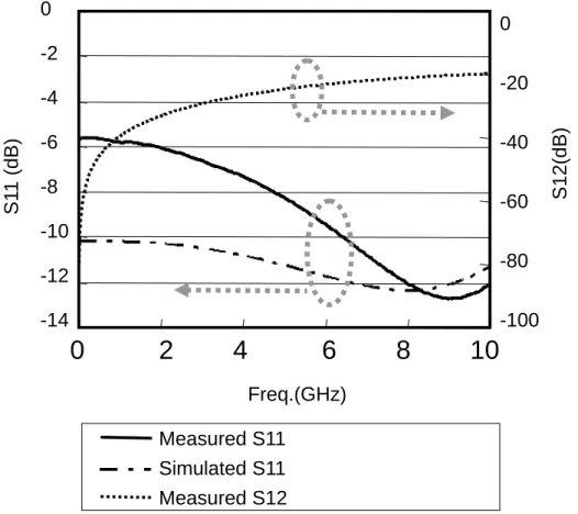
The measured S11 and measured S22 are shown in Fig. 3.10. S12 is better than
-20dB from 0 to 8GHz. Fig.3.11 shows the measured differential gain. According to the
simulated differential gain, the differential gain should have a pretty flat gain property.
The mean of the simulated differential gain is about -2dB. The variation of the
simulated differential gain is below ±0.5dB. We can observe the slop of the measured
differential gain increases. The variation of the measured differential gain increases to ±1.5dB. The parasitic inductance of 50fH at the third port output and the process variation cause this result.
For input impedance matching, using small resister R1 about 100Ω to let S11
this path to ground. Small resister R1 will causes lower differential gain and higher
noise figure. The simulated differential gain without R1 and the simulated noise figure
without R1 are shown in Fig. 3.12 and in Fig. 3.13, respectively. We can notice the
differential gain improve greatly and so does NF. The performance of this active balun
is summarized in Table 3.1. We can observe the advantages of the proposed active balun
are more wide bandwidth and less power consumption.
-6
-5
-4
-3
-2
-1
0
1
0
2
4
6
8
10
Freq. (GHz)
G
ai
n
di
ff
er
e
nc
e (
dB
)
simulation
measurement
Fig. 3.6. Measured data and simulation of gain difference.
172
174
176
178
180
182
0
2
4
6
8
10
Freq. (GHz)
P
h
as
e dif
fe
renc
e (
d
eg.
)
simulation
measurement
0
1
2
3
4
5
6
7
8
1
2
3
4
5
6
7
8
9
10
Freq. (GHz)
IIP
3
(d
B
m
)
Fig. 3.8. Measured IIP3 of the active balun.
0
2
4
6
8
10
12
0
2
4
6
8
10
Freq.(GHz)
NF(
d
B
)
Fig. 3.9. Measured NF-14 -12 -10 -8 -6 -4 -2 0
0 2
4
6
8
10
Freq.(GHz) S1 1 (dB) -100 -80 -60 -40 -20 0 S12(dB) Measured S11 Simulated S11 Measured S12Fig. 3.10. Measured S11 and Measured S12.
-4
-3
-2
-1
0
1
0
1
2
3
4
5
6
7
8
9 10
F req .(G H z)
Dif
fer
ent
ial G
ain (
dB
)
S im ulated D ifferential G ain
M eas ured D ifferential G ain
-3
-2.5
-2
-1.5
-1
-0.5
0
0.5
0
1
2
3
4
5
6
7
8
9
10
Freq.(GHz)
Dif
ferential Gain (dB)
Differential Gain with R1
Differential Gain without R1
Fig. 3.12. Simulated Differential Gain without R1.
0 1 2 3 4 5 6 7 8 9 10 0 1 2 3 4 5 6 7 8 9 10 Freq. (GHz) NF (d B ) NF with R1 NF without R1
TABLE 3.1 Summary of measured performance and comparison to other active balun
This work
[7]
MTT ‘98
[8]
ISCAS ‘03
Vdd 1.2V
3V
3V
Gain error
2dB
±1 dB
0.02 dB
Phase error
3 ° -1° 0.58
°
Freq.
~8 GHz
1.7 ~ 5.8 GHz
5.1 ~ 5.9 GHz
Power
consumption
1.44 mW
11.4 mW
9.17 mW
3.3 Improved Low Power Ultra-Wideband Active Balun
Discussed in section 3.2, the gain error and phase error rise when frequency
increase. According to the measurement result, we can find out two critical effects
cause this result. First is the measurement environment. As mentioned, the probe
parasitic are well calibrated for the two ports under test, the third port is terminated into
an un-calibrated probe. The unexpected parasitic greatly affects measurements accuracy,
especially for phase imbalance. It is found that by adding a parasitic inductance of 50fH
at the third port output, simulation data approaches to measurement data. But this issue
could be resolved by four-port measurements.
Second, unpredictable effects like process variation will affect the measurement
result, too. Process variation will affect the circuit itself and change the output loading
(the input impedance of the next stage). It is difficult to prevent this issue. So the active
balun with a tunable function to calibrate the mismatch from the process variation is
necessary.
And when active baluns combine with the next stage, the input impedance of the next
stage (the output loading of the active balun) may changes. So it is necessary to see the
variation of the gain difference and the phase difference when the RL in Fig. 3.14
changes. GD(200) and PD(200) mean the gain difference and the phase difference when
phase difference both increase when RL increases in Fig. 3.15. So we need to design a
tunable active balun for the output loading variation.
L
R
1
R2
R3
Mn(W/L )
Mp(3W / L )
C1
input
Out 1
Out
2
Vg
VaRL
RL
Fig. 3.14. Proposed active balun combined with the next stage.
-3.0 -2.5 -2.0 -1.5 -1.0 -0.5 0.0 0.5 1.0 1.5 2.0 0 2 4 6 8 10 Freq.(GHz) G a in D if fer ence (dB ) 166 168 170 172 174 176 178 180 182 184 186 P has e D if fer e nce (dB ) GD(200) GD(100) GD(50) GD(25) PD(200) PD(100) PD(50) PD(25)
Fig. 3.15. The simulated gain difference and phase difference with difference RL.
Vdd
Vdd
3.3.1 Design on 0~10 GHz Ultra Wide-Band Low Power
Tunable Active Balun for Loading Variation and Process
Variation Compensation
The tunable ultra wide-band active balun is shown in Fig. 3.16. According to Eq.
(3-3), as gm CgdnCgdp
2
2ω
>> in the frequency range of interest, the choice of R2 an R3
in Fig. 3.3 holds over a broad frequency range. Appropriate R2 and R3 can make
minimum gain and phase error over the desirable bandwidth. So, use an active
tunable resister M1 to replace R2 in Fig. 3.3 for tuning if it is necessary.
L
Vdd
R1
R3
Mn(W/L)
Mp(3W/L)
C1
RFin
Out1
Out2
Vg
Va
M1
V
tune
0
2
4
6
8
10
12
0
0.2
0.4
0.6
0.8
1
1.2
Vsd (volt)
Id
(
m
A
)
Fig. 3.17. PMOS I_V curve.
Vg Vs Vd Cgd Cgs Cdb Csb Rds(R2)
The PMOS M1 works in the triode region. The I_V curve of the PMOS is
shown in Fig. 3.17. On the triode region, MOS can be an active resister. When tuning
VSG of the PMOS, the value of the active resister Rds (
dId dVsd
) changes. The
equivalent model of the PMOS in the triode region shows in Fig. 3.18. Cgs and Csb of
PMOS M1 can be ignored because Vg and Vs in Fig. 3.17 connect to ground directly. Let Rds as R2 and Cgd//Cdb=C.
The small-signal equivalent circuit is as shown in Fig. 3.19. Critical to affect
output imbalance, the gate-drain parasitic capacitance, Cgd, shall be included in the
analysis. Derived from the core circuit, the common-source voltage, va, is related to the
gate voltage, vg, as gsp mp gsn mn gsn mn g a
sC
g
C
C
s
g
sC
g
v
v
+
+
+
+
+
=
)
(
1If the voltage v is one half of the gate voltage v , two outputs can reach a well-balanced (3-4)
V
inL
R
1C
gdnC
gsngm
nv
gv
aR
2//(
1/SC
)
R
3//(1/
SC
gdp)
C
gspgm
pv
o1v
o2condition. This leads to the requirement of gmn = gmp and C1+Cgsn = Cgsp. To do so, the
PMOS size is chosen as three times of the NMOS size. An external capacitor, C1, is also
added for the latter requirement. Under these conditions, the voltage ratio of the two
outputs is given by
As can be seen, the impedance matching components affect no gain and phase
imbalance. A balanced output demands vo1 = -vo2. If biasing current is large, then
gdn
m C
g >>ω and the condition is fulfilled. In low-power cases, the condition can be
fulfilled if the values of R2 and R3 follow these equations,
) ( 2 3 gdn gdp m gdn C C g C R − = , and m gdp gdn
g
C
C
R
R
2 3 22
1
1
≅
+
ω
. (3-6) As gm CgdnCgdp 2 2ω>> in the frequency range of interest, the choice of R
2 an
R3 holds over a broad frequency range. It concludes that the effect on imbalance from
the transistor parasitic is less than that from the compensation feedback and the current
source parasitic.
When process variation occurs, gain error and phase error will rise. Tuning the
gate voltage of the PMOS M1 to changes the value of R2 to minimize the mismatch.
Fig. 3.20 and Fig. 3.21 show phase difference and gain difference shift when the gate 3 3 2 2 2 1
2
1
1
)
1
//
(
1
)
2
1
)(
1
//
(
R
g
R
sC
sC
R
sC
sC
g
sC
R
v
v
m gdp gdn gdn m o o•
+
+
−
−
=
(3-5)voltage of the PMOS M1 changes. As the gate voltage of the PMOS M1 rise 0.1V,
gain difference and phase difference shift 1dB and 1.5°, respectively. According to the
simulated result, when the output loading changes from 25 to 200Ω, the improved
active balun still can achieves the desired performance. For constant DC power
consumption, the bottleneck of the DC current is on the PMOS Mp not PMOS M1. So,
-4 -3 -2 -1 0 1 2 3 4 0 2 4 6 8 10 Freq. (GHz) G a in D if fe re n c e (d B ) Vdd1=0.3V Vdd1=0.4V Vdd1=0.2V Vtune Vtune Vtune
Fig. 3.21. Gain difference vs. Vtune.
174 175 176 177 178 179 180 181 182 183 184 0 2 4 6 8 10 Freq. (GHz) P h as e D if fer enc e ( degr e e) Vdd1=0.3V Vdd1=0.4V Vdd1=0.2V Vtune Vtune Vtune
3.3.2 Microphotograph of Chip
A tunable balun circuit was designed in a standard 0.18um CMOS technology.
Fig. 3.22 shows the micrograph of the fabricated circuit. The total chip area is 0.5mm
by 0.68mm including bonding pads for on-wafer probing measurements. The area of
the core circuit could be much reduced in a fully integrated circuit. The RF input and
output ports are placed on the opposite sides of the chip to improve the isolation.
According to the last measurement result of the 8GHz ultra wideband active balun, we
find out there is the unaccounted parasitic at the gate-port of the PMOS resulting in
higher gain error. So adding bypass capacitors to prevent this issue.