利用單電荷現象研究高介電係數CMOS之加溫加壓回復效應與缺陷特性
61
0
0
全文
(2) 利用單電荷現象研究高介電係數 CMOS 之加溫加壓回復效應與缺陷特性 Investigation of BTI Recovery Effect and Trap Properties in High-k CMOS from Single Charge Phenomena 研 究 生 : 郭晉豪. Student : Jin-Hau Kuo. 指導教授 : 汪大暉 博士. Advisor : Dr. Tahui Wang. 國立交通大學 電子工程學系 電子研究所碩士班 碩士論文 A Thesis Submitted to Institute Electronics College of Electrical Engineering and Computer Science National Chiao Tung University in Partial Fulfillment of the Requirements for the Degree of Master of Science in Electronic Engineering June 2005 Hsinchu, Taiwan, Republic of China.. 中華民國 九十四 年 六 月.
(3) Investigation of BTI Recovery Effect and Trap Properties in High-k CMOS from Single Charge Phenomena. Student: Jin-Hau Kuo. Advisor: Dr. Tahui Wang. Department of Electronics Engineering & Institute of Electronics National Chiao Tung University. Abstract. This thesis investigates post BTI (Bias Temperature Instability) stress recovery effect in high-k gate dielectric. A fast transient measurement technique is developed to retrieve the missing information during switching between stress and recovery. In small-area transistors, we measured single electron de-trapping manifested by staircase-like drain current change during PBTI (Positive BTI) recovery. By characterizing the field and temperature effects on the single charge emission time, an analytical model based on tunneling is proposed. The high-k trap density and trap activation energy are extracted. Furthermore, the technique is applied to pMOSFETs with high-k and SiO2 as gate. ii.
(4) dielectric. Single hole emission is observed in both type of devices during NBTI (Negative BTI), and the responsible physical mechanism is identified to be similar to that for emission of trapped electrons. Finally, the recovery field, temperature (activation energy), and gate length effects are compared for combinations of dielectric and carrier; that is electrons in high-k nMOS, holes in high-k pMOS and holes in SiO2 pMOS.. iii.
(5) 利用單電荷現象研究高介電係數 CMOS 之加溫加壓回復效應與缺陷特性. 學生:郭晉豪. 指導教授:汪大暉 博士. 國立交通大學 電子工程學系. 電子研究所. 摘要 本論文主要研究高介電係數 CMOS 在高溫偏壓操作(BTI)後,元件特性回復 之現象。我們發展出一快速暫態的量測系統,可取得一般量測下因為施壓(stress) 和回復(recovery)狀態切換太慢而忽略的資料。在小面積元件的高溫正偏壓(PBTI) 實驗中,汲極電流呈現不連續的階梯變化,單一電子自陷阱釋放可明顯地量測出 來。藉著描述與電場及溫度有關的單一電子發射時間,一個與穿隧效應有關的有 效分析模型被提出。此高介電閘極元件之陷阱密度及陷阱活化能亦被取出。 此外,此技術亦可應用於高介電及二氣化矽之 p 型金氧半電晶體的實驗,在 此兩種元件的高溫負偏壓(NBTI)實驗中,可量測到單一電洞射出,而其相關物理 機制被證實與被補捉的電子釋放機制相似。最後,我們比較不同種類的元件與不 同載子(電子在高介電 n 型電晶體及電洞在高介電與二氧化矽 p 型電晶體)之相關 特性,例如回復電場,溫度(活化能),還有閘極長度效應等。. i.
(6) Acknowledgements I would like to express my deep gratitude to my advisor Dr. Tahui Wang for his patient guidance, encouragement and valuable discussion during the course of his study. I would like to express my sincere thanks to Chien-Tai Chan and TSMC Corporation who give me much assistance during the study of this work. In addition, I would like to express my deepest gratitude to my friends for their continuously emotional support during the course of this study. Finally, I would like to dedicate this thesis to my parents for their support and everlasting love.. iv.
(7) Contents Chinese Abstract. i. English Abstract. ii. Acknowledgements. iv. Contents. v. Figure Captions. vii. Chapter 1. 1. Introduction. Chapter 2 Single-Electron Emission of Traps in HfSiON. 5. 2.1. Introduction. 5. 2.2. Fast Transient Measurement. 5. 2.3. Single-electron emission time of traps in HfSiON. 6. 2.3.1. 6. Transient Recovery in Large Devices. 2.3.2 Single electron emission in small devices. 6. 2.4. Trapped electron emission mechanism. 7. 2.5. Analytical model. 7. 2.6. High-k trap density. 8. 2.7. Gate Length Effects. 9. 2.8 Modeling of PBTI Recovery Transient in a Large-area Device. 10. v.
(8) Chapter 3 Applications of the Transient Measurement Technique. 26. 3.1. Introduction. 26. 3.2. High-k Degradation: A Transient Analysis. 26. 3.3. NBTI Recovery Transient in pMOSFETs: High-k. 28. 3.4. Comparison among Different Gate Dielectrics. 28. Chapter 4. Conclusion. 43. Reference. 44. vi.
(9) Figure Captions Fig. 1.1 HfSiON nMOS with~2 orders gate current reduction.[1.4] Fig. 1.2 Typical Id-Vg hysteresis (Vt instability) in high-k nMOSFET. [1.11] Fig. 2.1 Experimental setup to measure high-k trapped charge emission times. In stress phase, Vg=0.7V, Vd=0V for 0.1s. In recovery phase, Vg=0.25~0.55V, and Vd=0.2V, and drain current temporal evolution is recorded by an digital oscilloscope. The high-speed switches minimize the delay between phase trasition down to µs. Fig. 2.2 Bias conditions for stress and recovery phases. Fig. 2.3 The photograph of the micro-second measurement system used in this work. Fig. 2.4. Stable current-time characteristics in oxide gate dielectrics ensure that this method induces no spurious current transient in HK.. Fig. 2.5 PBTI recovery transient, usually underestimated is significant. The recovery drain current follows logarithmic time dependence. Fig. 2.6 Pre-. and. Post-stress. current. evolutions. in. a. high-k. nMOSFET. with. W/L=0.16µm/0.08µm. The measurement bias is Vg=0.3V and Vd=0.2V. Each current jump in the post-stress recovery corresponds to a single trapped charge escape from the high-k gate dielectric. Only three electrons are trapped during stress. The charge emission times in recovery phase are denoted byτ1,τ2, andτ3 in the figure. Fig. 2.7 Gate voltage dependence of averaged high-k trapped charge emission times <τ1> and <τ2> in recovery phase. Ten measurements on the same device are made to take average. Fig. 2.8 Temperature dependence of <τ1>. The extracted activation energy is ~0.18eV. Fig. 2.9 Energy band diagram in recovery phase. Various charge escape paths are illustrated: (a) Frenkel-Poole (F-P) emission, (b) thermally-assisted-tunneling (TAT) to the gate,. vii.
(10) and (c) TAT to the Si substrate. From Vg dependence and temperature dependence of charge emission time in Fig.3 and Fig.4, only (c) should be considered. Fig. 2.10 Schematic representation of gate dielectric band diagram in recovery phase and trap positions. Ea is the activation energy for TAT, and the proposed model is described in detail in the text. Fig. 2.11 The ratio of τ2 to τ1 versus gate voltage in recovery phase. Note that τ2/ τ1 remains almost unchanged with respect to Vg. The extracted high-k trap density is also given. Totally, 10 devices are measured in the figure. Fig. 2.12 (a) Comparison of the current jump amplitude for Lgate=0.08µm and for Lgate=0.14µm. (b) The amplitude of charge escape induced current jump versus Lgate. Fig. 2.13 High-k, nMOS (W/L=100µm/0.08µm), continuous recovery trace. The calculated recovery transient (line) is in good agreement with experimental result (symbols). Fig. 3.1 Illustrations for four phases with bias conditions (a) stress phase, (b) discharge phase, (c) filling phase, and (d) recovery phase. Fig. 3.2 Electron quantum jump in small area devices (W/L=0.16µm/ 0.08µm) before and after positive Vg stress. Fig. 3.3 NMOS recovery Id traces in a large area device (W/L=100µm /0.08µm). The slope increases with stress time. Fig. 3.4 High-k trap density as a function of stress time. Fig. 3.5 (a) Device structure of high-k with EOT=18Å. (b) Device structure of oxide with EOT=20Å Fig. 3.6 Step-like channel current evolution during NBTI recovery in small area devices (W/L=0.16µm/0.08µm). τ1 and τ2 denote trapped hole emission times. Fig. 3.7 The Vg dependence of average trapped hole emission times, τ1 and τ2. Ten measurements on the same device are made to take average. Fig. 3.8 Temperature dependence of τ1. The extracted activation energy (Ea) from the Arrehnius plot is about 0.14eV.. viii.
(11) Fig. 3.9 The amplitude of measured current jump (∆Id) versus gate length. Fig. 3.10 Step-like. channel. current. evolution. during. recovery. in. (a)High-k. nMOS(W/L=0.16µm/0.08µm) (b)High-k pMOS (W/L=0.16µm/0.08µm) (c)Oxide nMOS (W/L=0.4µm/ 0.18µm) Fig. 3.11 The amplitude of measured current jump(△Id) versus gate length (a)High-k nMOS (b)High-k pMOS (c)Oxide pMOS Fig. 3.12 Vg dependence of average trapped charge emission times τ1,τ2 in recovery phase.(a)High-k nMOS (b)High-k pMOS (c)Oxide nMOS. Fig. 3.13 Temperature dependence of τ1 (a)Ea of High-k nMOS= 0.18eV (b)Ea of High-k pMOS=0.14eV (c)Ea of SiO2 pMOS=0.5eV. ix.
(12) Chapter 1 Introduction Metal oxide semiconductor field effect transistors (MOSFETs) have been continuously scaled since they were first developed in 1960s. To date, The Silicon dioxide (SiO2) is always chosen for MOSFETs’ gate dielectrics material. With technology scaling, the thickness of gate dielectric has to be made progressively smaller. Scaling of gate dielectric thickness is for the purpose of improving transistor performance, but it increases quantum mechanical direct tunneling leakage current [1.1]. The standby power consumption thus increases to an intolerable level. To solve this problem, high permittivity (high-k) materials are emerged as a post-SiO2 solution [1.2]. Effort of research groups around the globe is now focusing on hafnium-based materials, exploring the nature of these materials extensively, like the film composition, process optimization, reliability assessment and analysis [1.3-1.6]. Recently, HfSiON has been successfully integrated into CMOS as gate dielectrics for low power applications, with good reliability, comparable mobility (as SiO2) and significantly reduced gate leakage [1.4]. Figure.1.1 shows the gate leakage, Jg, for HfSiON samples used in this work, versus that for SiO2 with several equivalent oxide thicknesses (EOT) [1.4]. The leakage is lower for the HfSiON samples, than for SiO2 of similar EOT. Although high-k materials have been regarded as good replacement for SiO2 gate dielectric devices, there are still challenges for implementing high-k dielectric. One of these challenges is stress-induced Vt-instability behavior [1.7-1.10]. Compared with SiO2, hafnium-based oxides show significant threshold voltage shift due to charging 1.
(13) of the pre-existing traps [1.8-1.9]. Figure.1.2 illustrates Id-Vg characteristics of the nMOS transistor obtained after positive voltage stress for various stress times [1.11]. Stress increases the threshold voltage but it does not degrade the sub-threshold slope. Figure.1.2 leads us to the conclusion that the threshold voltage shift is due to trapping of the charges in the bulk of the dielectric. BTI (bias temperature instability) effect was observed for SiO2 gate dielectrics long ago [1.12]. On one hand, unlike SiO2 where NBTI (negative bias temperature instability) in pMOS dictates lifetime extrapolation [1.13], high-k dielectric suffers from PBTI (positive bias temperature instability) in nMOS which is believed to be essentially related to charge trapping in high-k [1.14]. On the other hand, similar to NBTI in SiO2, both PBTI degradation (charge trapping) and recovery (charge de-trapping) are being studied [1.14]. In Chapter 2, we study properties of the traps in HfSiON by characterizing single electron emission during PBTI recovery with a novel transient measurement technique. By exploring the post-stress recovery transient of drain current in small devices, an analytical model based on tunneling is developed. According to the model, high-k trap density and trap activation energy are extracted. In Chapter 3, the drain current recovery transient in a large-area device is successfully reproduced with the analytical model developed in Chapter 2. In addition, NBTI in HfSiON and in SiO2 are also investigated. Single charge (electron for PBTI, and hole for NBTI) emission is compared among the three conditions. Finally, we give a conclusion in Chapter 4.. 2.
(14) 3. 10. Inversion |Vg|=1.2V. 1. 10. -1. Jg (A/cm2). 10. Oxide nMOS. -3. 10. HfSiON nMOS 1.8nm. -5. 10. -7. 10. 0.5. 1.0. 1.5. 2.0. 2.5. 3.0. EOT(nm). Fig.1.1. HfSiON nMOS with~2 orders gate current reduction.[1.4]. 3. 3.5.
(15) Fig.1.2. Typical Id-Vg hysteresis (Vt instability) in high-k nMOSFET. [1.11]. 4.
(16) Chapter 2 Single-Electron Emission of Traps in HfSiON. 2.1 Introduction The cause of BTI is believed to be essentially related to charge trapping in high-k [2.1, 2.2]. BTI is commonly characterized by stressing transistors at a high temperature and electric field, periodically interrupting the stress to monitor threshold voltage and/or drain current. The other way to investigate BTI effect is to measure post-stress recovery behavior [2.3]. To identify the charge de-trapping mechanism, a novel method for characterizing high-k gate dielectric is demonstrated, in which direct measurement of single-electron de-trapping manifested by discontinuous step-like drain current is measured. The physical path of de-trapping can be identified accordingly. An analytical model based on tunneling can predict the emission time behavior, and gives the high-k trap density.. 2.2 Fast Transient Measurement The trapped charge behavior in high-k gate dielectric is studied by “stress” and “recovery” as shown in Fig. 2.1, where the temporal evolution of drain current is recorded by a digital oscilloscope and the time delay during phase transition is minimized by high-speed switches down to µs. The sampling rate is 104 readings per second. Fig. 2.2 illustrates the bias conditions applied the gate and drain. During the stress phase, electrons in the inversion channel are injected into the high-k bulk traps. During the recovery phase, trapped electrons discharge. Fig. 2.3 shows the photography of our micro-second transient measurement circuit.. 5.
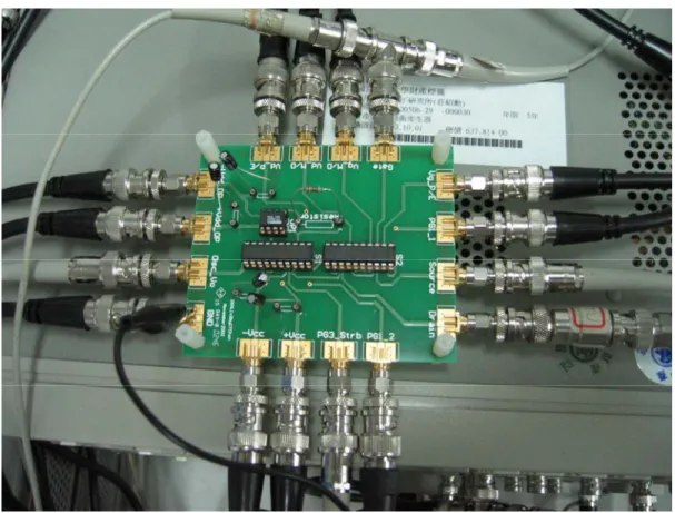
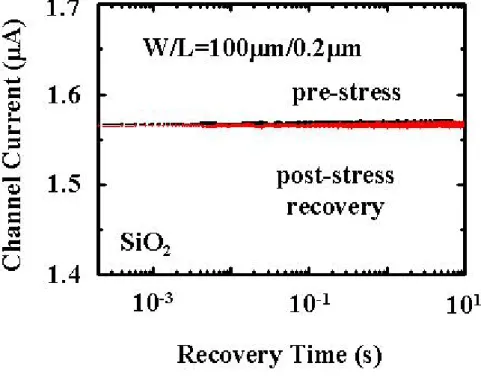
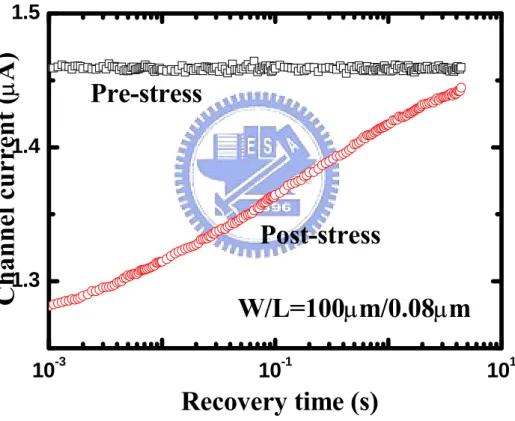
(17) 2.3 Single-Electron Emission Time of Traps in HfSiON The transient measurement setup is tested on MOSFETs with SiO2 as gate dielectric, stable current-time characteristics (Fig. 2.4) ensure that this method induces no spurious current transient. 2.3.1 Transient Recovery in Large Devices. The device has an area of 100µm*0.08µm. As shown in Fig. 2.5, after stress (Vg=0.7V, 0.2s) is removed, Id increases with logarithmic time dependence during recovery (Vg/Vd=0.3/0.2V) and saturates to a level close to the pre-stress one, suggesting full recovery for the chosen stress condition. Notably, the observation time window extends four decades from 1ms to 10s. In traditional measurements, it takes a minimum delay for seconds between stress and recovery during which a significant portion of recovery is happening (Fig. 2.5). Transient measurement is demonstrated to be necessary for accurate analysis. 2.3.2 Single Electron Emission in Small Devices. In a large area device, the recovery Id represents a collective effect of numerous traps in high-k and rises smoothly with recovery time (Fig. 2.5). While the same experiment (identical stress and recovery conditions) is conducted on a small (W/L=0.16µm/0.08µm) device where only a few traps are present, the recovery Id, interestingly, exhibits a staircase-like evolution, as indicated in Fig. 2.6. In this study, each drain current step corresponds to a “single” electron de-trapping from the high-k dielectric. Interestingly, the time of occurrence for each electron de-trapping (i.e. τ1, τ2, and τ3) (or referred to as emission time) increases with Vg applied in “recovery” (Fig. 2.7). Ten measurements of each Vg bias on the same device were made to take average. Furthermore, as expected, the emission time of electron de-trapping is found to decrease at elevated temperatures (Fig. 2.8). The activation energy extracted from the Arrehnius plot is about 0.18eV. The experimental results will be used to identify 6.
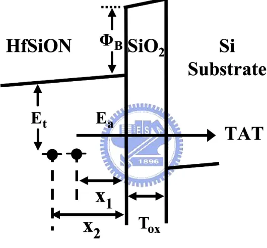
(18) the mechanism of electron de-trapping in high-k gate dielectric as discussed in the next section.. 2.4 Trapped Electron Emission Mechanism There are three possible paths for electron de-trapping as illustrated in the energy band diagram in Fig. 2.9, i.e. Frenkel-Poole (F-P) emission (path a), tunneling (path b) toward the gate electrode, and tunneling toward the Si substrate (path c). The de-trapping path (a) is ruled out, since the activation energy for F-P mechanism should be equal to the trap energy, Et (>1eV), and the extracted Ea is only 0.18eV. The de-trapping path (b) is ruled out too since a larger Vg would accelerate the electron emission toward the gate electrode resulting in a shorter emission time. The observed trend is just the opposite (Fig. 2.7). Initially, we attempted to use direct tunneling for describing electron de-trapping. However, it fails to account for the field and temperature effect due to lack of relevant parameters in its formalism. Moreover, Leroux et al. successfully modeled hysteresis in high-k by utilizing SRH kinetics in their calculation [2.4]. Consequently, a SRH-like thermally-assisted-tunneling (TAT) is incorporated in our model and will be given in detail in the next section. Temperature dependence (Fig. 2.8) with extracted activation energy of 0.18eV confirms the role of thermal process in charge emission.. 2.5 Analytical Model An analytical model of the TAT mechanism is developed with energy band diagram and trap distance illustrated in Fig. 2.10:. (2.1). τ i−1 = υ exp( −α oxTox ) exp( −α k x1 ). 7.
(19) where. υ = [ N c (1 − f c )]υ th [σ 0 exp(. α ox =. * 2 2mox q ( Et + Φ B ). =. − Ea )] kT. ;α k =. (2.1a). 2 2mk* qEt. (2.1b). =. Eq. (2.1) reveals the nature of tunneling for trapped electron emission time, τi. The pre-factor υ, a lumped parameter referred to as the “attempt-to-escape frequency” can be re-written as in Eq. (2.1a) [2.3] where NC is the effective density-of-state in the Si conduction band, NC(1-fc) is the amount of available states in Si substrate for out-tunneling electrons from high-k traps, σ0 and Ea represent the trap cross-section and the activation energy. Other variables have their usual definitions. The Fermi-Dirac distribution (fc) in the Si conduction band is a function of Vg in “recovery.” A smaller recovery Vg leads to a lower surface carrier density (a smaller fc) and thus a shorter electron emission time. As the recovery Vg drops below the threshold voltage (Vt), decrease in the emission time tends to saturate since fc approaches zero. The electron nearest to the interface of Si substrate will be the first one for de-trapping to occur. With respect to the temperature effect, a small recovery Vg (<0.25V), where fc~0, was chosen for measurement of the trap activation energy to exclude the temperature dependence of fc, as shown in Fig. 2.8. The extracted activation energy from the Arrhenius plot is 0.18eV.. 2.6 High-k Trap Density The high-k trap density can be evaluated through the analytical model, Eq. (2.1). By comparing. 8.
(20) τ 1 = υ −1 exp(α oxTox ) exp(α k x1 ) τ 2 = υ −1 exp(α oxTox ) exp(α k x2 ) we obtain. τ2 = exp[α k ( x2 − x1 )] τ1. (2.2). and the high-k trap density (Nt) is readily calculated as. Nt =. 1 1 = ( x2 − x1 )WL WL 1 ln(τ 2 ). αk. (2.3). τ1. Eq. (2.2) predicts that the ratio of emission times (e.g. τ2 to τ1 ) is only related to the physical distance of trap sites away from the interface. Fig.2.11 indeed shows the ratio of τ2/τ1 (10 readings of each gate bias on the same device) is constant and independent of recovery Vg. The average high-k trap density calculated from Eq. (2.3) (assuming m*k ~0.18m0 [2.5]) is 3.5*1017cm-3, or equivalently, an areal density of 8.8*1010cm-2. This small trap density can hardly be resolved by CP due to a comparable interface trap density [2.6]. It should be pointed out that the extracted trap density, according to Eq. (2.3), is not affected by variables such as Tox, m*ox and Ea. The total available number of traps in high-k gate dielectric of each device for the stress (electron filling) condition is related to high-k thickness, trap density, and transistor size. The observed 3 electrons trapped in the nMOS after the “stress” in this study are less than the total traps (~10) as calculated from the estimated trap density and transistor size.. 2.7 Gate Length Effects. 9.
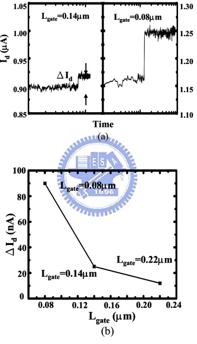
(21) The experiment was conducted on devices with different gate lengths, 0.08µm, 0.14µm, and 0.22µm. It is found that while step-like current recovery traces due to single-electron de-trapping are still observed for all lengths, the amplitude of the drain current step (∆Id) decreases with longer gate lengths, as shown in Fig.2.12. This trend is consistent with the Random Telegraph Signal (RTS) theory [2.7] and implies that the impact of the trapped electron in the high-k dielectric spreads over the entire channel. Thus, a single-electron emission can be observed only when the device size is small enough and the high-k is clean enough!. 2.8 Modeling of PBTI Recovery Transient in a Large-area Device In a large area device, the high-k charge de-trapping rate is. Q( x, t ) = Q( x,0) exp[-t / τ( x )]. (2.4). where Q(x,t)=qNt(x,t) is the time-dependent trapped charge density and τ(x) is described in Eq. (2.1). The threshold voltage shift ∆Vt induced by trapped electron emission can be written as. ∆Vt ( t ) = ∑ i. qN t ( x i ,0) ∆Q( x i , t ) -t =∑ (THK - x i )[1 - exp( )] C( x i ) ε HK τi i. (2.5). where C(xi) is the corresponding capacitance for trapped charges located at xi from high-k/IL interface, and εHK and THK are permittivity and physical thickness of the high-k layer respectively. For a large amount of trapped charges, the summation in Eq. (2.5) can be replaced by an integration,. x. ∆Vt ( t ) =∫ 0. qN t ( x,0) (THK - x ){1 - exp[-t/τ(x)]}dx. ε HK. 10. (2.6).
(22) where τ(x)=Aexp(αkx) and A=[NC(1-fc)νthσ0exp(-Ea/kT)]-1exp(αoxTox). Because the double exponential exp[-t/τ(x)]=exp[(-t/A)exp(-αkx)] in the integrand changes abruptly from 0 to 1 around x=(αk)-1ln(t/A), it can be approximated by a step-function: 0 for x ≤ (α k ) -1 ln( t / A) t exp[(- ) exp(-α k x )] = { 1 for x ≥ (α k ) -1 ln( t / A) A. (2.7). This approximation translates into a “clear-cut” picture; after time t, electrons with emission times shorter than t are completely de-trapped while all of the rest remain trapped. Therefore, Eq. (2.6) is further simplified,. ∆Vt ( t ) ≈. qN t ε HK. ( α k ) -1 ln( t / A ). ∫0. (2.8). (THK - x )dx.. The time window of interest for modeling is four decades as indicated in Fig. 2.13. According to Eq. (2.2), the time span is equivalent to a physical distance of around 10Å in high-k, or an equivalent oxide thickness (EOT) of 2Å. Therefore, the term THK-x in Eq. (2.8) is approximated as a constant, or xeff, and Eq. (2.8) reduces to. ∆Vt ( t ) ≈. qN t x eff t ln( ). ε HK α k A. (2.9). The corresponding recovery drain current evolution can be written as. ∆I d ( t ) ≈. - qG m N t x eff t ln( ). ε HK α k A. (2.10). where Gm(=dI/dV) is the transconductance. Using the extracted Nt and Ea from a small device, the simulated recovery transient from Eq. (2.10) is shown in Fig. 2.13 11.
(23) and is in good agreement with the measured result. Eq. (2.10) also reveals that the recovery slope in Fig. 2.13 is directly correlated to the high-k trap density. The injected electrons may fill different energy traps at larger stress Vg. In this case, the trap energy distribution should be taken into account and Eq. (2.10) is modified as follows. ∆I d (t ) ∝ ∫. - qG m N t ( Et ) xeff ∆E. ε HK α k ( Et ). dEt ln(t ). (2.11). where ∆E represents the energy range of trapped charges. ∆Id(t) still follows log-time dependence. Finally, the authors would like to remark that we chose a very short stress time (0.2s) in this study. The purpose is to characterize the pre-existing high-k traps only.. 12.
(24) Stress. Recovery. Recovery. Stress. G D. Fig. 2.1. I/V Converter. S. Oscilloscope. Experimental setup to measure high-k trapped charge emission times. In stress phase, Vg=0.7V, Vd=0V for 0.1s. In recovery phase, Vg=0.25~0.55V, and Vd=0.2V, and drain current temporal evolution is recorded by an digital oscilloscope. The high-speed switches minimize the delay between phase trasition down to µs.. 13.
(25) Stress Vg G S. Recovery. Vd. D. Fig. 2.2 Bias conditions for stress and recovery phases.. 14.
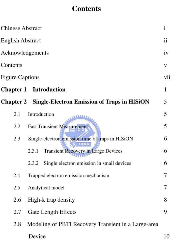
(26) Fig. 2.3 The photograph of the micro-second measurement system used in this work.. 15.
(27) Fig. 2.4. Stable current-time characteristics in oxide gate dielectrics ensure that this method induces no spurious current transient in HK.. 16.
(28) Channel current (µA). 1.5. Pre-stress. 1.4. Post-stress. 1.3. W/L=100µm/0.08µm -3. 10. -1. 10. 1. 10. Recovery time (s). Fig. 2.5. PBTI recovery transient, usually underestimated is significant. The recovery drain current follows logarithmic time dependence.. 17.
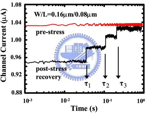
(29) Channel Current (µA). 1.08. W/L=0.16µm/0.08µm 1.04. pre-stress 1.00 0.96. post-stress recovery. 0.92. τ1. τ2. τ3. 0.88 10-3. Fig. 2.6. 10-2. Time (s). 10-1. 100. Pre- and Post-stress current evolutions in a high-k nMOSFET with W/L=0.16µm/0.08µm. The measurement bias is Vg=0.3V and Vd=0.2V. Each current jump in the post-stress recovery corresponds to a single trapped charge escape from the high-k gate dielectric. Only three electrons are trapped during stress. The charge emission times in recovery phase are denoted byτ1,τ2, andτ3 in the figure.. 18.
(30) High-K Charge Emission Time (s) Fig. 2.7. 1. ⟨τ2⟩ ⟨ τ1 ⟩. 0.1. 0.25. 0.35. 0.45. 0.55. Recovery Gate Voltage (V) Gate voltage dependence of averaged high-k trapped charge emission times <τ1> and <τ2> in recovery phase. Ten measurements on the same device are made to take average.. 19.
(31) 〈τ1〉(s). 0.1. Recovery Vg/Vd=0.3V/0.2V. Extracted Ea~0.18eV. 0.01 2.8. Fig. 2.8. 3.2. 3.0. 3.4. 1000/T (K-1). Temperature dependence of <τ1>. The extracted activation energy is ~0.18eV.. 20.
(32) Fig. 2.9. Energy band diagram in recovery phase. Various charge escape paths are illustrated: (a) Frenkel-Poole (F-P) emission, (b) thermally-assisted-tunneling (TAT) to the gate, and (c) TAT to the Si substrate. From Vg dependence and temperature dependence of charge emission time in Fig.3 and Fig.4, only (c) should be considered.. 21.
(33) HfSiON. Et. Φ B SiO. 2. Ea. Si Substrate TAT. x1 x2 Fig. 2.10. Tox. Schematic representation of gate dielectric band diagram in recovery phase and trap positions. Ea is the activation energy for TAT, and the proposed model is described in detail in the text.. 22.
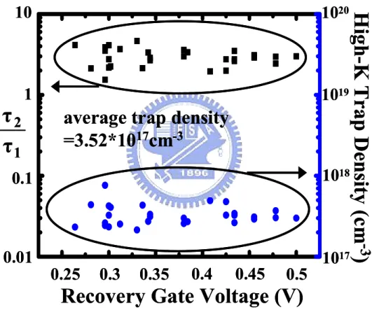
(34) 1020. 1. 1019. τ2 τ1. average trap density =3.52*1017cm-3. 0.1. 1018. 0.01. 1017. 0.25. 0.3. 0.35. 0.4. 0.45. 0.5. High-K Trap Density (cm-3). 10. Recovery Gate Voltage (V) Fig. 2.11. The ratio of τ2 to τ1 versus gate voltage in recovery phase. Note that τ2/ τ1 remains almost unchanged with respect to Vg. The extracted high-k trap density is also given. Totally, 10 devices are measured in the figure.. 23.
(35) 1.05. 1.30. Id (µA). Lgate=0.14µm 1.00. Lgate=0.08µm. ecovery rrecovery Vg/Vd=0.3V/0.2V. 1.25. 0.95. 1.20. ΔId 0.90. 1.15. 0.85. 1.10. Time (a). 100. Lgate=0.08µm. ΔId (nA). 80 60 40. Lgate=0.22µm. 20 0. Fig. 2.12. Lgate=0.14µm 0.08. 0.12. 0.16. Lgate (µm) (b). 0.20. 0.24. (a) Comparison of the current jump amplitude for Lgate=0.08µm and for Lgate=0.14µm. (b) The amplitude of charge escape induced current jump versus Lgate.. 24.
(36) Channel Current (µA). 1.5 pre-stress. 1.4 1.3 10-3. Fig. 2.13. post-stress recovery Symbol: measurement Line: simulation. 10-1 Recovery Time (s). 101. High-k, nMOS (W/L=100µm/0.08µm), continuous recovery trace. The calculated recovery transient (line) is in good agreement with experimental result (symbols).. 25.
(37) Chapter 3 Applications of the Transient Measurement Technique 3.1 Introduction In Chapter 2, the electron traps in HfSiON nMOSFETs have been characterized, and based on the experimental results we proposed an analytical model responsible for high-k trapped charge de-trapping. We can accordingly evaluate the trap density either from the current quantum jumps measurement or from drain current recovery slope. The activation energy can also be extracted by de-trapping the charges at different temperatures. In this chapter, firstly, high-k degradation effect is studied by both experimental techniques (current jumps and recovery slope). We introduce a four-phase experimental procedure: stress-discharge-filling-recovery. After the high-k film is degraded, both the number of current jumps and the recovery slope for drain current change, indicating trap growth. Secondly, the technique developed for exploring single electron phenomena is utilized to investigate properties of hole traps during NBTI recovery in pMOSFETs with high-k and SiO2 as gate dielectric. The effects of gate length, recovery gate voltage, and temperature are compared between different carrier types (electron traps vs. hole traps) and between different materials (high-k vs. SiO2).. 3.2 High-k Degradation: A Transient Analysis To investigate high-k degradation effect, we propose a four-phase experimental procedure: stress, discharge, filling and recovery. Fig. 3.1 illustrates the bias conditions for the four phases respectively. In the “stress” phase (Fig. 3.1a), a large 26.
(38) positive Vg is applied with all other terminals grounded to damage and generate additional traps in the gate dielectric. The devices are then “discharged“ at a negative Vg (-1.5V, 20s), shown in Fig. 3.1b. Following that, the devices are subjected to “filling” (Fig. 3.1c) immediately followed by “recovery” (Fig. 3.1d) (fast switching by the circuit in Fig.2.1). The recovery drain current change is monitored and recorded for further analysis. The “discharge” phase is required to empty (as much as possible) the trapped charges introduced during the stress phase which may probably lead to incorrect results from the “filling” and “recovery” phases. The filling and recovery conditions are exactly identical to those in Chapter. 2 (termed as “stress and recovery” in Chapter 2, though). Fig. 3.2 shows the recovery drain currents in high-k nMOSFETs before and after a constant voltage stress at Vg=3.5V for 500s. The device area is W*L=0.16*0.08µm2. According to (2.3) in Chapter 2, the trap density can be obtained by two equivalent ways. One fixes the numerator as unity (one interval between two traps) and the trap density can be calculated once the ratio of emission times is known. The other fixes the denominator (here, two decades, from 0.01s to 1s) and the trap density can be calculated as well simply by counting the number of current jumps within the pre-set window. The latter is suitable for the case where the recovery patterns are complicated, or more jumps. Indicated in Fig.3.2, the pre-stress curve has only one current jump while the post-stress one has five jumps. Increase in the number of current jumps corresponds to increase in trap density as a result of constant voltage stress. On the other hand, recovery drain current slope is demonstrated to be directly correlated to trap density in gate dielectric in Chapter 2 (section 2.8). Fig. 3.3 indicates the change in recovery slope with stress time. Again, increase in slope corresponds to increase in trap density as a result of constant voltage stress. The trap growth rate is extracted as shown in Fig. 3.4. 27.
(39) 3.3 NBTI Recovery Transient in pMOSFETs: High-k Fig. 3.5 illustrates the device structures used for comparison in this and the next section. The EOT is 1.8nm and 2nm for high-k and for SiO2 respectively. Fig.3.6 shows the drain current evolution during recovery for small-area high-k pMOSFETs (W/L= 0.16µm/0.08µm). Similar to that in its nMOS counterparts, the drain current transient exhibits staircase-like current discontinuities. Each current jump here is believed due to a single trapped hole emission from traps in high-k. While the Vg for filling holes into the high-k gate dielectric is -0.8V, the Vg needed for injecting holes into SiO2 devices (see section 3.4) is larger than -1.5V. Therefore, the possibility of de-trapped charges from the interfacial SiO2 layer is excluded since for the Vg (-0.8V) used there is no holes injected into the interfacial SiO2 layer. The trapped holes are de-trapped from high-k. The dependence of charge emission times on recovery gate voltage (Fig. 3.7) and temperature (Fig. 3.8) are measured, and the trend is similar to those for trapped electrons (Chapter 2), only different in relative dependence. This confirms similar de-trapping mechanism for both trapped electrons in nMOS and trapped holes in pMOS. The extracted activation energy for trapped holes is 0.14eV, slightly smaller than that for trapped electrons (0.18eV, Fig. 2.7). The gate length effect is also measured as indicated in Fig. 3.9.. 3.4 Comparison among Different Gate Dielectrics Single hole de-trapping is observed in SiO2-gated pMOSFETs [3.1], shown in Fig. 3.10c. The Vg and temperature effects are also measured. Fig. 3.11 compares the dependence of the current jump amplitude (△Id) on gate length. The recovery drain voltage is kept at 0.2V for all lengths in all devices in order to alleviate Vd effect [3.2]. For all cases, shorter devices have larger current jump amplitude. The large current 28.
(40) jump amplitude for electrons than holes regardless of dielectric material is probably due to smaller mobility for holes [3.2]. Fig. 3.12 shows similar recovery Vg dependence for all cases, stronger for nMOS, though. It proves that both electron and hole emission path is from gate dielectric to channel both in HfSiON and SiO2 for the chosen charge-injection condition. Fig. 3.13 demonstrates the temperature effect of τ1. The activation energy of HfSiON nMOS (0.18eV) and pMOS (0.14eV) are comparable, and higher in SiO2 pMOS (0.5eV, Fig. 3.13c), indicating that the activation energy is dependent on the material type, not on the carrier type.. ]. 29.
(41) Vg=3.5V. Vg =-1.5V. G. G. S. S. D. D. (b) Discharge phase. (a) Stress phase. Vg=0.7V. Vg=0.3V Vd=0.2V. G. G D. S. S. (c) Filling phase. Fig. 3.1. D. (d) Recovery phase. Illustrations for four phases with bias conditions (a) stress phase, (b) discharge phase, (c) filling phase, and (d) recovery phase.. 30.
(42) 2.10. Id(µA). 2.05 2.00. W/L=0.16µm/0.08µm. Fresh device. 1.95. High-k nMOS. 1.90 1.85 0.01. 0.1. 1. Time(s). 2.35. Id(µA). 2.30 2.25 2.20. W/L=0.16µm/0.08µm. Stress condition Vg=3.5V 500s High-k nMOS. 2.15 2.10 0.01. 0.1. 1. Time(s) Fig 3.2. Electron quantum jump in small area devices (W/L=0.16µm/ 0.08µm) before and after positive Vg stress.. 31.
(43) 1.6. Id (µA). W/L=100µm/0.08µm. 1.4. 1s 100s 1.2. 1E-3. stress condition: Vg=3.5V, 25C. 2000s. 0.01. 0.1. 1. 10. Time (s). Fig 3.3. NMOS recovery Id traces in a large area device (W/L=100µm /0.08µm). The slope increases with stress time.. 32.
(44) Nt (*1011cm-2). W/L=100µm/0.08µm 10. stress condition: Vg=3.5V, 25C. 1 10. 100. 1000. Stress Time (s) Fig 3.4. High-k trap density as a function of stress time.. 33.
(45) Poly-Si HfSiON SiO2. (a). Poly-Si SiO2 (b). Fig 3.5. (a)the device structure of High-k with EOT=18Å (b)the device structure of Oxide with EOT=20Å. 34.
(46) 2.05. Id(µA). W/L=0.16µm/0.08µm 2.00. 1.95. τ1 1.90 -3 10. High-k pMOS. τ2 -2. -1. 10. 10. 0. 10. Time(s) Fig. 3.6. Step-like channel current evolution during NBTI recovery in small area devices (W/L=0.16µm/0.08µm). τ1 and τ2 denote trapped hole emission times.. 35.
(47) 0. Emission time (s). 10. -1. 10. <τ2>. High-k pMOS. <τ1>. -2. 10. -0.6. -0.7. -0.8. -0.9. Recovery Gate Voltage (V). Fig. 3.7. The Vg dependence of average trapped hole emission times, τ1 and τ2. Ten measurements on the same device are made to take average.. 36.
(48) Ea=0.14. -2. <τ1>(s). 10. High-k pMOS -3. 10. 2.8. 3.0. -1. 3.2. 3.4. 1000/T (K ). Fig. 3.8. Temperature dependence of τ1. The extracted activation energy (Ea) from the Arrehnius plot is about 0.14eV. 37.
(49) 40. Lgate=0.08µm ∆Id(nA). 30. Lgate=0.14µm. 20. 10. 0. High-k pMOS. Lgate=0.22µm. 0.10. 0.15. 0.20. Lgate(µm) Fig. 3.9. The amplitude of measured current jump (∆Id) versus gate length.. 38.
(50) 1.08. W/L=0.16µm/0.08µm. Id(µA). 1.04 1.00. (a). 0.96 0.92 0.88 -3 10. High-k nMOS. τ2 τ3. τ1 -2. -1. 10. 0. 10. 10. Time(s). 2.05. Id(µA). W/L=0.16µm/0.08µm 2.00. (b). 1.95. τ1 1.90 -3 10. High-k pMOS. τ2 -2. -1. 10. 0. 10. 10. Time(s). (c). W/L=0.4µm/0.18µm. Id(µA). 1.32. 1.29. 1.26. 1.23 1E-3. τ2. τ1 0.01. 0.1. Oxide pMOS 1. Time(s). Fig 3.10. Step-like channel current evolution during recovery in (a)High-k nMOS(W/L=0.16µm/0.08µm) (b)High-k pMOS (W/L=0.16µm/0.08µm) (c)Oxide nMOS (W/L=0.4µm/ 0.18µm). 39.
(51) 100. Lgate=0.08µm ∆Id(nA). (a). High-k nMOS. 80. 60. 40. Lgate=0.14µm. 20. Lgate=0.22µm 0. 0.08. 0.12. 0.16. 0.20. 0.24. Lgate(µm). 40. Lgate=0.08µm. High-k pMOS. (b). ∆Id(nA). 30. Lgate=0.14µm. 20. 10. Lgate=0.22µm 0. 0.10. 0.15. 0.20. Lgate(µm). 50. ∆Id(nA). (c). Oxide pMOS. Lgate=0.12µm. 40 30 20. Lgate=0.24µm 10 0. Lgate=0.2µm 0.12. 0.16. 0.20. 0.24. Lgate(µm). Fig 3.11. The amplitude of measured current jump(△Id) versus gate length (a)High-k nMOS (b)High-k pMOS (c)Oxide pMOS. 40.
(52) Emission time (s). (a). 1. <τ2> <τ1>. 0.1. High-k nMOS. 0.3. 0.4. 0.5. Recovery Gate Voltage (V). 0. (b). Emission time (s). 10. -1. 10. <τ2> <τ1>. High-k pMOS. -2. 10. -0.6. -0.7. -0.8. -0.9. Recovery Gate Voltage (V). 0. (c). Emission time (s). 10. <τ2> -1. 10. <τ1>. Oxide pMOS. -2. 10. -0.1. -0.2. -0.3. -0.4. Recovery Gate Voltage (V). Fig 3.12. Vg dependence of average High-k trapped charge emission times τ1,τ2 in recovery phase.(a)High-k nMOS (b)High-k pMOS (c)Oxide nMOS.. 41.
(53) 0.1. (a). τ1(s). Ea=0.18eV. High-k nMOS. 0.01. 2.8. 3.0. 3.2. 3.4. 1000/T (K-1). 0.1. τ1(s). (b). Ea=0.14eV. High-k pMOS 0.01 2.8. 3.0. 3.2. 3.4. -1. 1000/T (K ). (c). τ1(s). 0.1. Ea=0.5eV 0.01. 2.8. Oxide pMOS 3.0. 3.2. 3.4. 1000/T (K-1). Fig 3.13. Temperature dependence of τ1 (a)Ea of High-k nMOS= 0.18eV (b)Ea of High-k pMOS=0.14eV (c)Ea of SiO2 pMOS=0.5eV. 42.
(54) Chapter 4 Conclusion A fast transient measurement setup and technique is developed in this work. The technique is firstly used to study PBTI recovery transient in HfSiON nMOSFETs. Single electron emission from traps in HfSiON gate dielectric is observed in small-size devices. Based on the characterization of recovery field and temperature effects on the single electron phenomena, a SRH-like thermally-assisted-tunneling model for trapped charge emission is proposed. The model well explains the experimental results and the prediction it makes is verified by measurement. The extracted trap activation energy is 0.18eV. Results from large- and small-size devices are well correlated. It is found that the trap density can be evaluated self-consistently from the ratio of trapped charge emission times (small devices) and from drain current recovery slope (large devices). The recovery transient for a large-area device is also well reproduced and follows logarithmic time dependence. Furthermore, the technique is applied to pMOSFETs with high-k and SiO2 as gate dielectric for single hole analysis. Comparison shows the emission mechanism is universal for transient electron/hole de-trapping in high-k and SiO2. It is also found that the role of thermal process (activation energy) depends on material type (high-k or SiO2), not on carrier type (electron or hole). The proposed technique is a powerful tool to characterize traps in gate dielectric for advanced CMOS.. 43.
(55) Reference Chapter 1 [1.1] J. H. Stathis, D. J. DiMaria, “Reliability projection for ultra-thin oxides at low voltage”, IEDM Tec. Dig., pp. 167-170 1998 [1.2] H. Iwai, S. Ohmi, S. Akama, C. Ohshima, A. Kikuchi, I. Kashiwagi, J. Taguchi, H. Yamamoto, J. Tonotani, Y. Kim, I. Ueda, A. Kuriyama, Y. Yoshihara, “Advanced gate dielectric materials for sub-100nm CMOS”, IEDM Tech. Dig., pp. 625-628,2002 [1.3] J. C. Lee, H. J. Cho, C. S. Kang, S. Rhee, Y. H. Kim, R. Choi, C. Y. Kang, C. Choi, M. Abkar, “High-k dielectrics and MOSFET characteristics”, IEDM Tech. Dig., pp. 95-98, 2003 [1.4]. H.C.-H. Wang, S.-J. Chen, M.-F. Wang, P.-Y. Tsai, C.-W. Tsai, T.-W. Wang, S.M. Ting, T.-H. Hou, P.-S. Lim, H.-J. Lin, Y. Jin, H.-J. Tao, S.-C. Chen, C.H. Diaz, M.-S. Liang, and C. Hu, “Low power device technology with SiGe channel, HfSiON, and poly-Si gate”, IEDM Tech. Dig., pp. 161-164, 2004. [1.5]. A. S. Oates, “Reliability issues for high-k gate dielectrics”, IEDM Tech. Dig., pp. 923-926, 2003. [1.6]. R. Degraeve, A. Kerber, P. Roussell, E. Cartier, T. Kauerauf, L. Pantisano, G. Groeseneken, “Effect of bulk trap density on HfO2 reliability and yield”, IEDM Tech. Dig., pp. 935-938, 2003. [1.7]. K. Onishi, C. S. Kang, R. Choi, H.-J. Cho, S. Gopalan, R. Nieh, S. Krishnan,. 44.
(56) and J. C. Lee, “Charging effects on reliability of HfO2 devices with polysilicon gate electrode”, Proc. IEEE Int. Reliability Physics Symp., pp.419–420, 2002 [1.8]. S. Zafar, A. Callegari, E. Gusev, and M. V. Fischetti, “Charge trapping related threshold voltage instabilities in high permittivity gate dielectric stacks”, J. Appl. Phys., vol. 93, no.11, pp. 9298–9303, 2003.. [1.9]. A. Kreber, E. Cartier, L. Pantisano, M. Rosmeulen, R. Degraeve, T. Kauerauf, G. Groeseneken, H. E. Maes, and U. Schwalke, “Characterization of the VT-instability in SiO2 =HfO2 gate dielectrics,” Proc. IEEE Int. Reliability Physics Symp., pp. 41–45, 2003. [1.10] E. P. Gusev and C. P. D’Emic, “Charge detrapping in HfO2 high-k gate dielectric stacks,” Appl. Phys. Lett., vol. 83, no. 25, pp. 5223–5225, 2003. [1.11]. A. Shanware, M. R. Visokay, J. J. Chambers, A. L. P. Rotondaro, H. Bu, M. J. Bevan, R. Khamankar, S. Aur, P. E. Nicollian, J. McPherson, L. Colombo,” Evaluation of the Positive Biased Temperature Stress Stability in HfSiON Gate Dielectrics”, Proc. IEEE Int. Reliab. Phys. Symp., pp. 208-213,2003. [1.12]. B. E. Deal, M. Sklar, A. S. Grove, and E. H. Snow, “Characteristics of the surface-state charge of thermally oxidized silicon”, J. Electrochem. Soc., vol. 114, pp. 266–274, 1967.. [1.13]. N. Kimizuka, T. Yamamoto, T. Mogami, K. Yamaguchi, K. Imai, and T. Horiuchi, “The impact of bias temperature instability for direct-tunneling. 45.
(57) ultra-thin gate oxide on MOSFET scaling”, VLSI Tech. Dig. pp. 73-74, 1999 [1.14]. C. Shen, M.F. Li, X.P. Wang, H.Y. Yu, Y.P. Feng, A.T.-L. Lim, Y.C. Yeo, D.S.H. Chan, and D.L. Kwong, “Negative U Traps in HfO2 Gate Dielectrics and Frequency Dependence of Dynamic BTI in MOSFETs”, IEDM Tech. Dig., pp.733-736, 2004. 46.
(58) Chapter 2 [2.1]. A. Shanware, M. R. Visokay, J. J. Chambers, A. L. P. Rotondaro, H. Bu, M. J. Bevan, R. Khamankar, S. Aur, P. E. Nicollian, J. McPherson, and L. Colombo, “Evaluation of the positive biased temperature stress stability in HfSiON gate dielectrics”, Proc. Int. Reliab. Phys. Symp., pp. 208-213, 2003. [2.2]. C. Shen, M.F. Li, X.P. Wang, H.Y. Yu, Y.P. Feng, A.T.-L. Lim, Y.C. Yeo, D.S.H. Chan, and D.L. Kwong, “Negative U Traps in HfO2 Gate Dielectrics and Frequency Dependence of Dynamic BTI in MOSFETs”, IEDM Tech. Dig., pp.733-736, 2004. [2.3]. Rangan, S.; Mielke, N.; Yeh, E.C.C.,”Universal recovery behavior of negative bias temperature instability”, Electron Devices Meeting, 2003. IEDM '03 Technical Digest. IEEE International 8-10 Dec. 2003 P.age(s):14.3.1 - 14.3.4. [2.4]. C. Leroux1, J. Mitard1,2, G.Ghibaudo3, X. Garros1, G. Reimbold1, B. Guillaumot2, F. Martin1, “Characterization and modeling of hysteresis phenomena in high K dielectrics”, IEDM Tech. Dig., pp.737-740, 2004. [2.5]. Y. T. Hou, M. F. Li, H. Y. Yu, Y. Jin, and D.-L. Kwong, “Quantum Tunneling and Scalability of HfO2 and HfAlO Gate Stacks”, proceedings of International Electron Device Meeting, pp. 731-734., 2002. [2.6]. R. Degraeve, A. Kerber, Ph. Roussel, E. Cartier, T. Kauerauf, L. Pantisano, and G. Groeseneken, “Effect of Bulk Trap Density on HfO2 Reliability and. 47.
(59) Yield”, proceedings of International Electron Device Meeting, 2003, pp. 935-938. [2.7]. M.-H. Tsai, T. P. Ma, and T. R. Hook, “Channel Length Dependence of Random Telegraph Signal in Sub-Micron MOSFETs”, IEEE Electron Device Letter, Vol. 15, NO. 12, pp. 504-506, 1994.. 48.
(60) Chapter 3 [3.1]. C. T. Chan, H. C. Ma, C. J. Tang, and Tahui Wang, "Investigation of Post-NBTI Stress Recovery in pMOSFETs by Direct Measurement of Single Oxide Charge De-Trapping", accepted, Symp. on VLSI Tech., 2005. [3.2]. M.-H. Tsai, T. P. Ma, and T. R. Hook, “Channel Length Dependence of Random Telegraph Signal in Sub-Micron MOSFET’s”, IEEE Electron Device Letter, Vol. 15, NO. 12, pp. 504-506, 1994.. 49.
(61) 簡. 歷. 姓名: 郭晉豪 性別: 男 生日: 民國 70 年 4 月 11 日 籍貫: 台灣嘉義縣 地址: 嘉義縣竹崎鄉灣橋村崎腳 97 號 學歷: 國立中央大學物理系. 88.9-92.6. 國立交通大學電子工程研究所碩士班 92.9-94.6 碩士論文題目:. 利用單電荷現象研究高介電係數 CMOS 之加溫加壓回復效應與缺陷特性. Investigation of BTI Recovery Effect and Trap Properties in High-k CMOS from Single Charge Phenomena. 50.
(62)
數據

+7

相關文件
structure for motion: automatic recovery of camera motion and scene structure from two or more images.. It is a self calibration technique and called automatic camera tracking
ADSL(A symmetric D igital S ubscriber L ine ,非對稱數位
The aim of this study is to investigate students in learning in inequalities with one unknown, as well as to collect corresponding strategies and errors in problem solving..
In order to investigate the bone conduction phenomena of hearing, the finite element model of mastoid, temporal bone and skull of the patient is created.. The 3D geometric model
Kwong, “Metal nanocrystal memory with high-k tunneling barrier for improved data retention, ” IEEE Trans. Electron
第二章是介紹 MEMS 加工製程,包括體型微加工、面型微加工、LIGA、微 放電加工(Micro-EDM)、積體電路相容製造技術 CMOS MEMS 製程等。製作微 加速度感測器。本研究是選用台積電 0.35μm
譚志忠 (1999)利用 DEA 模式研究投資組合效率指數-應用
The purposes of this research was to investigate relations among learning motivation, learning strategies and satisfaction for junior high school students, as well as to identify
