Diamond and Related Materials 9 (2000) 1249–1256
www.elsevier.com/locate/diamond
Comparative studies on field emission properties
of carbon-based materials
K.H. Chen
a,*, J.-J. Wu a, L.C. Chen b, C.Y. Wen b, P.D. Kichambare b, F.G. Tarntair c,
P.F. Kuo
d, S.W. Chang d, Y.F. Chen d
a Institute of Atomic and Molecular Sciences, Academia Sinica, Taipei, Taiwan b Center for Condensed Matter Sciences, National Taiwan University, Taipei, Taiwan c Department of Electronic Engineering, National Chiao Tung University, Hsinchu, Taiwan
d Department of Physics, National Taiwan University, Taipei, Taiwan
Abstract
Comparative studies on field emission properties of various carbon-related materials including diamond, amorphous carbon, SiCN films, SiCN nanorods, and carbon nanotubes are presented. While diamond is well known for its potential use in cold cathodes, the emission current of a hydrogen-treated diamond film is relatively small compared to that of amorphous carbon or diamond-like-carbon film. Meanwhile, carbon nanotubes have demonstrated large emission currents at much lower threshold voltages, showing their potential for applications. However, the emission from carbon nanotubes is subjected to significant decay under long-term operation. The emission current and long-term stability can be improved using a new SiCN compound with nanorod morphology. The effective barrier height and the field enhancement factor derived from the Fowler–Nordheim equation are discussed in this paper. © 2000 Elsevier Science S.A. All rights reserved.
Keywords: Amorphous carbon; Carbon-based materials; Carbon nanotubes; Diamond; Field emission properties; SiCN films; SiCN nanorods
1. Introduction With the advent of nanometer materials such as carbon
nanotubes, the carbon-based electron field emitter expe-rienced another rush, bringing the idea of cold-cathode In the past few years, considerable interest has been
focused on the electron field emission from diamond closer to reality.
In this report, a comparison of materials produced and related materials [1–3]. Due to its negative electron
affinity property, diamond has been widely recognized in our laboratory ranging from bias-assisted carburized (BAC ) silicon tips [8], SiCN nano-crystallite [9,10], as the dream material for various applications from cold
cathodes, flat panel displays, to a new generation of SiCN nanorods [11], and carbon nanotubes [12] is made to elucidate the mechanisms of field emission. The microwave tubes. Experimental data, however, indicate
that non-diamond phases such as diamond-like carbon correlations of the material, the field enhancement factor (geometry of the sample) and the effective barrier height (DLC ), amorphous carbon (a-C ), and other
nanostruct-ural carbon demonstrate a much better field-emission (work function) to the emission current are investigated. property than that of diamond [4,5]. The addition of
dopants into the material can substantially reduce the onset field from 30 V/mm typically to a few V/mm, and
2. Experimental
can enhance the emission current up to hundreds of mA/cm [2,6 ]. It has been demonstrated that the
introduc-2.1. Sample preparation
tion of an sp2 phase in the film further reduces the onset field intensity and enhances the emission current [7].
A silicon microtip array (50×50 square and 1 mm in width) of each tip was produced by standard photo-lithography and reactive ion etching processes. The
* Corresponding author. Fax:+886-2-2362-0200.
E-mail address: [email protected] ( K.H. Chen) ultra-high aspect ratio cone-shaped microtip array was
0925-9635/00/$ - see front matter © 2000 Elsevier Science S.A. All rights reserved. PII: S 0 9 25 - 9 63 5 ( 9 9 ) 00 3 5 2- 0
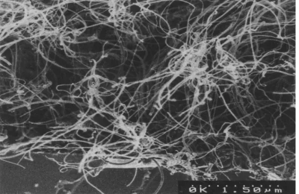
Fig. 1. Typical SEM micrograph of carbon nanotubes.
further coated with a carbon layer using the BAC a pressure of 50 Torr and a substrate temperature of 900°C. The Fe catalytic layer is patterned to form a process. Selective deposition of the carbon layer on the
surface of sharp silicon tips was achieved by careful 50×50 array of 8 mm squares with 16 mm spacing. After 30 min of deposition, we observed multi-wall tubes of adjustment of the bias voltage and bias time. The
optimal conditions for the BAC were −200 V bias 10 mm in length and 20–50 nm in diameter with a random orientation ( Fig. 1).
voltage for 40 min with 25%CH
4in H2using a
micro-wave plasma CVD reactor at a substrate temperature The growth of SiCN films has been described in detail elsewhere [13]. In short, an electron cyclotron of 650°C. Typically, sharp tips of 50 nm radius were
produced for the emission study. resonance (ECR) plasma CVD reactor operating at a microwave power of 1200 W with a gas ratio of The carbon nanotubes in this study were deposited
using microwave plasma enhanced CVD operated at CH3NH2:SiH4:N2:H2=50:1:125:125 and a silicon sub-strate temperature of 700°C was utilized to deposit 1.5 kW. An n-type Si substrate was first deposited with
300 A˚ Fe and then nanotube growth was continued in nano-crystalline SiCN films of 300 nm thick on a silicon substrate. The typical stoichiometry of the SiCN films the CVD reactor with 20 sccm CH4 and 80 sccm H2 at
1251
K.H. Chen et al. / Diamond and Related Materials 9 (2000) 1249–1256
thus deposited was (Si;C )
3N4with Si/C ranging from 1 is a high-resolution field emission SEM, allowing a magnification of up to 300 000. The composition of the to 2. The films thus deposited had a hexagonal structure
with typical lattice constants of a=7.70 A˚, and c= sample was analyzed by a Perkin Elmer scanning Auger nanoprobe system (SAN760), which allows depth profile 5.78 A˚ .
In addition to the crystalline films described above, data to be acquired from an area as small as 500 A˚ . Further composition and chemical bonding information SiCN exhibited another phase of reduced
dimensional-ity. By using a proprietary buffer layer of 30 nm before were determined by X-ray photooelectron spectroscopy ( XPS ) using a Perkin Elmer Phi 1600 ESCA system. regular MWPE-CVD, one-dimensional SiCN rods of
20–60 nm with an aspect ratio of 50 were deposited. A MgKa radiation with an energy of 1253.6 eV was used as the source with a linewidth of 0.7 eV. Depth profiling high-resolution SEM image of the SiCN nanorods is
shown in Fig. 2, indicating well-faceted nanorods with with the XPS was performed by 4 kV Ar ion-beam bombardment of the sample.
a six-sided cross-section. The detailed growth mechanism and characteristics of the SiCN nanorods are not included in this paper and will be reported elsewhere
[11]. 3. Results and discussion
3.1. Emission from BAC silicon tips 2.2. Field emission measurement
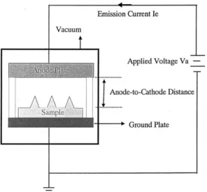
The field emission characteristics were obtained using Typical emission characteristics from the 50×50 BAC silicon tips are shown in Fig. 4. A turn-on field of standard I–V measurement under a high vacuum with
a base pressure of 2×10⁻⁷ Torr, as given in Fig. 3. A 20 V/mm and an emission current of 120 mA at 36.7 V/mm were achieved. The F–N plot in the inset of Fig. 4 gave rectangular graphite electrode of 2×3 cm2 was placed
30 mm above the sample. A Keithely multimeter was an effective barrier height of 0.017 eV, assuming a field enhancement factor of 31.6 from geometrical calcula-employed for sourcing the voltage and measuring the
current. Precautions were taken to clean the sample tions. Note that the total current instead of current density is specified in this case due to the fact that it is before measurement in order to eliminate any dust
particles on the surface that might have caused false an array of tips instead of a plain uniform film in our study. Therefore, it is meaningless to compare the cur-signals. During the measurement, the voltage increase
was adjusted to allow a detailed study of the I–V rent density as in the latter cases in this paper. In practical applications, the total current divided by the characteristics. The option to hold the voltage and
record the emission current at a constant voltage makes number of tips yielding the emission current per tip provides the most meaningful values.
possible, emission stability measurement, which is important for practical applications.
3.2. Emission from carbon nanotubes 2.3. Other characterization
Typical emission characteristics of carbon nanotubes are shown in Fig. 5, in which a turn-on field strength of The morphology of the films was analyzed using a
Hitachi scanning electron microscope (S-5000), which 10 V/mm and a maximum current of 3.8 mA at 16.7 V/mm were demonstrated. Multiple emission peaks were observed in Fig. 5, indicating emission site damage in the film and the subsequent appearance of newer emis-sion sites at higher voltages, which is quite common in most carbon-nanotube samples. The phenomenon that several groups of emission sites coexist in a carbon-nanotube sample can be attributed to the different height of the nanotube, various diameters, and the different curvature or different types of tubes. Further studies are needed to determine the role of each factor on the emission at different stages. The F–N plot in the inset of Fig. 5 shows multiple emission groups, of which each individual group showed a linear relationship that fol-lows the F–N equation.
Taking into account a total number of 2500 squares in each array and a 64 mm2 area for each square, one obtains a current density of 2.6 A/cm2 at 16.7 V/cm,
Fig. 4. Field emission I–V curve and the corresponding F–N plot (inset) of 50×50 BAC silicon microtip arrays.
other materials at a comparable field. It still needs to from three samples of composition ratios [C ]:[Si ]:[N ] of 22:21:57, 13:32:55, and 0:41:59, respectively. It is be verified whether a larger-area carbon-nanotube
sample will have the same performance as the array- quite clear that carbon incorporation into the film is essential for the field emission enhancement. Meanwhile, type sample. None the less, the arrayed carbon
nano-tubes demonstrate a great potential for various electron the origins of signal oscillation that occurs at a high applied field are still unclear and will be investigated sources applications including that for microwave
devices. further. The F–N plots in Fig. 6 show different slopes for samples of various composition, which can be attrib-uted to the different barrier heights of the films.
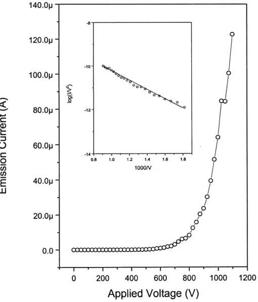
3.3. Emission from SiCN films
The electron emissions of three SiCN films are shown 3.4. Emission from SiCN nanorods
in Fig. 6, in which a turn-on field of 13 V/mm and a
maximum current density of 0.7 mA/cm2 at 36.7 V/mm Fig. 7 shows the emission characteristics of a SiCN nanorod sample. Compared to that of SiCN films, a have been demonstrated. The current density is relatively
small, compared with that of carbon nanotubes. higher emission current of 1.5 mA/cm2 at 35 V/mm with a turn-on field of 10 V/mm was observed. The enhance-However, the 0.7 mA/ cm2emission current density is
several orders of magnitude higher than that of ordinary ment in emission properties can be attributed to the geometric factor of the nanorod structure as well as the silicon or diamond films. The three sets of data from
1253
K.H. Chen et al. / Diamond and Related Materials 9 (2000) 1249–1256
Fig. 5. Field emission I–V curve and the corresponding F–N plot (inset) of an array containing the 50×50 squares of carbon nanotubes.
composition/structure of the material. Remarkably, the density, J (A/m2), F=bV/d with voltage, V (volts), F–N plot in the inset of Fig. 7 shows an excellent linear distance, d (m), w, the effective barrier height in (eV ), relationship over the entire range of applied field, indi- and b the field enhancement factor that depends on the cating ideal field emission characteristics. emitter geometry. Since there are only two parameters, The Fowler–Nordheim description of the field emis- b and w, in this equation, a linear fit in the F–N plot sion can be expressed as allows us to derive the field enhancement factor as well as the effective barrier height of the emitter, which can provide an insight into the physics of the field emission.
J=AF2
w exp
A
−Bw3/2F
B
, (1) However, the current density in the Fowler–Nordheim equation is often not well defined due to the ambiguity in the emission area, which is difficult to determine where A=0.014 and B=6.8×10⁹ are constants. Themorphol-Fig. 6. Field emission I–V curve and the corresponding F–N plot (inset) of three SiCN films with composition ratios [C ]:[Si ]:[N ] of 22:21:57(&), 13:32:55($), and 0:41:59(+).
ogy like nano-crystallites, nanotubes, and nanorods. 3.5. Stability comparison of the carbon nanotubes and SiCN nanorods
Therefore, there are three unknown parameters, b, w, and the emission area, in the Fowler–Nordheim equation
instead of two parameters as mentioned earlier. While achieving the highest emission current at the lowest applied field is the goal in most field emission Apparently, a linear fit in F–N plot only provides two
parameters, slope and intersection, from which it is not studies, the long-term stability of the emission is also an essential issue to be addressed. A comparison of the possible to determine all the unknown parameters.
Therefore, instead of providing the key parameters, b emission stability of a carbon-nanotube sample and a SiCN-nanorod sample is shown in Fig. 8. Although the and w, an F–N plot can only be used to exemplify the
cur-1255
K.H. Chen et al. / Diamond and Related Materials 9 (2000) 1249–1256
Fig. 7. Field emission I–V curve and the corresponding F–N plot (inset) of SiCN nanorods.
rent (3.8 mA for an array of 50×50 squares), the be wise to define the emission stability by the stressed emission at either specific current densities or at a emission current decayed to 15% of the initial value
after 1000 s of operation. In contrast, the SiCN nanorods specific applied field. showed a lower emission current (1.5 mA/cm2), but the
decay was much slower, about 50% decay after 1000 s
of operation. It should be pointed out that the stability 4. Conclusion
measurement has not been standardized so far. In our
case, an operating condition near the maximum emission Among the four types of materials studied for electron field emission, carbon nanotubes deposited by current is chosen for the test. The decay characteristics
will be very different if we choose another test condition MWPECVD demonstrated the highest emission current, which is several orders of magnitude higher than that such as half the emission current. Therefore, it would
Acknowledgements
Financial support for this project from National Science Council, Taiwan, under contract no. NSC-88-2113-M-001-021 and NSC-88-2112-M-002-022 is gratefully acknowledged. Two of the authors, Dr J.J. Wu and Dr P.D. Kichambare acknowledge the postdoctoral fellowship awarded by the National Science Council, Taiwan
References
[1] C. Wang, A. Garcia, D.C. Ingram, M.E. Kordesh, Electron. Lett. 27 (1991) 1459.
[2] M.W. Geis, N.N. Efremov, J.D. Woodhouse, M.D. McAleese, M. Marchywka, D.G. Socker, J.F. Hochedez, IEEE Electron Device Lett. 12 (1991) 456.
[3] M.W. Geis, J.C. Angus, Sci. Am. (1992) 84 October.
[4] W. Zhu, G.P. Kochanski, S. Jin, L. Seibles, J. Appl. Phys. 78 (1995) 2707.
[5] B.S. Satyanarayana, A. Hart, W.I. Milne, J. Robertson, Appl. Phys. Lett. 71 (1997) 1430.
Fig. 8. Long-term stability of the field emission of SiCN nanorod ($) [6 ] K. Okano, S. Koizumi, S. Ravi, P. Silva, G.A.J. Amaratunga, and carbon nanotubes (&). Nature 389 (1996) 140.
[7] L. Diederich, O.M. Kuttel, P. Aebi, L. Schlapbach, Diamond Relat. Mater. 8 (1999 ) 743.
[8] P.D. Kichambare, F.G. Tarntair, L.C. Chen, K.H. Chen, H.C.
of diamond films. However, SiCN films and nanorods
Cheng, J. Vac. Sci. Tech. (1999) (communication).
showed a moderate emission current, which is compara- [9] L.C. Chen, T.R. Lu, C.T. Kuo, D.M. Bhusari, J.J. Wu, K.H. ble to most of the ‘good’ emitters. However, the stability Chen, T.M. Chen, Appl. Phys. Lett. 72 (1998) 3449.
of the emitters should be emphasized to meet the require- [10] L.C. Chen, C.Y. Yang, D.M. Bhusari, K.H. Chen, M.C. Lin, J.C. Lin, T.J. Chuang, Diamond Relat. Mater. 5 (1996) 514.
ment of practical applications. Moreover, the issue of
[11] K.H. Chen, J.J. Wu, S.L. Wei, C.Y. Wen, L.C. Chen, P.F. Kuo,
deriving an effective barrier height and the field
enhance-Y.F. Chen, in: Handbook of Advance Electronic and Photonic
ment factor in Fowler–Nordhiem equation is addressed.
Materials, H.S. Nalwa ( Ed.). Academic Press, in press.
It is concluded that a definitive effective emission surface [12] T.W. Ebbesen, P.M. Ajayan, Nature 358 (1992) 220.
area is needed to solve the F–N equation completely [13] K.H. Chen, J.J. Wu, C.Y. Wen, L.C. Chen, C.W. Fan, P.F. Kuo, Y.F. Chen, Thin Solid Films 355–356 (1999) 205.

![Fig. 6. Field emission I–V curve and the corresponding F–N plot (inset) of three SiCN films with composition ratios [C ]:[Si ]:[N ] of 22:21:57(&), 13:32:55($), and 0:41:59(+).](https://thumb-ap.123doks.com/thumbv2/9libinfo/7525667.119261/6.892.123.752.80.790/field-emission-curve-corresponding-inset-films-composition-ratios.webp)

![Fig. 8. Long-term stability of the field emission of SiCN nanorod ($) [6 ] K. Okano, S](https://thumb-ap.123doks.com/thumbv2/9libinfo/7525667.119261/8.892.96.393.70.442/fig-long-stability-field-emission-sicn-nanorod-okano.webp)
