24-GHz 互補式金氧半導體電流操作模式
射頻前端接受器之設計
研究生:詹豪傑 指導教授:吳重雨 博士
國立交通大學
電子工程學系 電子研究所碩士班
摘 要
本論文提出一個創新的高頻電路設計概念,電流操作模式。並且設計一個操 作頻率在 24-GHz 電流操作模式射頻前端接收器,透過國家晶片系統設計中心委 託台灣積體電路製造股份有限公司以 0.13 微米互補式金氧半導體製程技術來實 現。此射頻前端接收器包含的電路有電流操作模式的低雜訊放大器和電流操作模 式的降頻器。整個電流操作模式的射頻接收器已經被完整的設計、製造與量測完 成。 量測結果顯示,此射頻前端電路可良好地工作在 24-GHz 的操作頻率,但由 於電路佈局上的疏失,量測結果的效能不如當初所預期。在經由雙束型聚焦離子 束的補救之後,射頻前端接收器的功率增易為 12.5dB,雜訊指數為 13.3dB,1dB 增易壓縮點為-15dBm,在 1.2V 的操作電壓下共消耗了 41.5mA。THE DESIGN OF 24-GHz CMOS CURRENT-MODE
RECEIVER FRONT-END
Student: Hao-Jie Zhan Advisor: Dr. Chung-Yu Wu
Department of Electronics Engineering & Institute of Electronics
National Chiao Tung University
Abstract
A new 24-GHz RF CMOS current-mode receiver integrated with a current-mode LNA and a current-mode downconverter has been proposed and fabricated in a 0.13-um CMOS technology supported by Taiwan Semiconductor Manufacturing Company via Chip Implementation Center. The proposed receiver is completely designed, fabricated and measured.
The measured results exhibit that the receiver can operate well at 24-GHz frequency range. But is doesn’t achieve adequate performance due to the oversight of layout. After the FIB solution, the fabricated current-mode receiver has conversion gain of 12.5dB, noise figure of 13.3 dB, a 1-dB compression point of -15 dBm, and drains 41.5mA under 1.2 supply voltage with chip area of 1mm2.
誌 謝
能夠順利畢業,要感謝的人真的很多。首先,我要對我的指導教授吳重雨老 師致上最誠摯的感謝。感謝老師在這兩年中,不論在硬體或軟體資源提供我一個 最佳學習環境。並且在學習上,老師適時指導與啟發,使我不在錯誤中打轉,更 教導了我許多做事的方法與態度。 再來我要感謝實驗室的學長蕭碩源、周忠昀、王文傑、余繼堯、蘇烜毅、陳 旻珓、黃祖德、歐欣華、粘家熒,在這兩年中給予了我許多研究上的幫助與指導, 使得我的論文能更佳的出色。還有我要實驗室的同學與學弟們:怡凱、志遠、汝 玉、必超、仲朋、允賓、豐維、昌平、泰翔、芳綾、佳惠、資閔、志賢、立龍、 國慶、柏宏、順維、晏維、 國忠...等,在這兩年中我們一起研究功課、遊山 玩水,使我的碩士兩年的生活更多采多姿。 最後我要感謝我的女朋友靖雯,謝謝你在這兩年碩士生活中陪伴我走過許多 人生的低潮。在我研究上遇到瓶頸時,你的鼓勵與支持讓我走過種種一切的不如 意;在我忙碌於研究時,你總是默默的陪伴在我身邊替我加油,讓我能無後顧之 憂的向成功邁進。 其他要感謝的人還有很多,無法一一列出,在此一併謝過。豪傑
于 風城交大
95 年 秋
CONTENTS
Chinese Abstract...i
English Abstract...ii
Contents...iv
Table Captions...vi
Figure Captions...vii
CHAPTER 1 INTRODUCTION
1.1 Background
……….1
1.2
A Review of CMOS RF Receiver Front-End………...2
1.2.1 High-Frequency CMOS LNA circuit………...…4
1.2.2 CMOS Down-Conversion……….……….10
1.3 Motivation
....………...………..16
1.4 Thesis
Organization...16
CHAPTER 2 CIRCUIT DESIGN AND SIMULATION
RESULTS
2.1
Current-Mode Low-Noise Amplifier...18
2.1.1 Operational Principle and Design Consideration...18
2.1.1.1 Input Matching Network……….19
2.1.1.2 Noise and Linearity……….21
2.2
Current-Mode Down-Conversion Mixer………...33
2.2.1 Operational Principle and Design Consideration ...……….34
2.2.1.1 Current Summing Circuit.…...………..35
2.2.1.2 I-square circuit...36
2.2.2 Circuit Implementation ...42
2.3
Simulation Results ...45
CHAPTER 3 EXPERIMENTAL RESULTS
3.1 Layout
Description...60
3.2 Measurement
Considerations and Setup...62
3.3 Experimental
Results...66
3.4
Discussions and Comparisons...73
CHAPTER 4 CONCLUSIONS AND FUTURE WORK
4.1 Conclusions...78
4.2 Future
Work...78
Reference...79
Table Captions
Table(i) Detail parameters of the current-mode LNA...33
Table(ii) Detailed parameters of current-mod downconverter...44
Table(iii) The comparison with previously reported LNA for frequencies around 20-GHz...52
Table(iv) The corner of the post-simulation summary...58
Table(v) Post-simulation summary with temperature variation... 59
Table(vi) Comparison on bias status between post-simulation and measurement ...71
Table(vii) Summary of the measurement results... 72
Table(viii) Summary of the measurement results with different supply voltage...73
Table(ix) Summary of revised post-simulation results... 76
Figure Captions
Fig. 1 Common receiver architecture... 3
Fig. 2 Single transistor amplifier [3]... 4
Fig. 3 Common-gate amplifier used a cascode transistor in the LNA [4] ... 5
Fig. 4 The input impedance analysis of cascode LNA... 5
Fig. 5 The high frequency effect of the cascode LNA topology [6]... 7
Fig. 6 The simplified schematic of 3-stage common-source LNA [7]... 7
Fig. 7 Common-gate with resistive feedthrough LNA. (a) Schematic. (b) Small-signal equivalent circuits [8]... 8
Fig. 8 Three stage LNA with a CGRF topology as the first stage [8]...9
Fig. 9 (a) A simple switch used as a mixer, (b) implementation of switch with a NMOS device... 11
Fig. 10 Gilbert cell mixer. (a) single-balanced, (b) double-balanced... 12
Fig. 11 Schematic diagram of single-balanced mixer with current bleeding...13
Fig. 12 The simplified schematic of single-end transconductance mixers. (a) gate-pumped mixer. (b) drain-pumped mixer... 13
Fig. 13 Simplified circuit diagram of the single-gate quadrature balanced mixer [10]...14
Fig. 14 Simplified circuit schematics of the passive drain-pumped resistive mixer [11]...15
Fig. 15 Block diagram of the current-mode receiver front-end... 17
Fig. 16 Current-mirror amplifier with inductor feedback. (a) schematic (b) small signal equivalent circuits... 20
Fig. 17 The standard CMOS small signal noise model [13]... 23
Fig. 18 The simplified small signal noise model... 25
Fig. 19 The noise source distribution of the input stage... 26
Fig. 21 The setup of NFmin versus VGSsimulation... 28
Fig. 22 The simulation result of minimum noise figure versus VGS... 29
Fig. 23 The simulation result of dB(S(2,1)) versus VGS...29
Fig. 24 The transconductance of transistor device... 31
Fig. 25 The complete schematic of current-mode LNA... 32
Fig. 26 The block diagram of current-mode mixer... 34
Fig. 27 The current summing circuit... 35
Fig. 28 The simplified current squaring circuit...36
Fig. 29 Conversion gain and 1dB compression point of current-mode downconverter...38
Fig. 30 The impact of difference of VDS voltage...40
Fig. 31 The difference of drain current of between the modified quadratic equation of VGS-Vt and model definition...41
Fig. 32 The complete whole circuit of I-square circuit... 42
Fig. 33 The complete circuit of the current-mode circuit... 44
Fig. 34 Simulation result S11 of LNA...46
Fig. 35 Simulation result S22 of LNA... 46
Fig. 36 Simulation result S21 of LNA... 47
Fig. 37 Simulation result S12 of LNA... 47
Fig. 38 Simulation result NFmin of LNA... 48
Fig. 39 Linearity simulation result P1dB of LNA... 48
Fig. 40 Simulation result of conversion gain of LNA... 49
Fig. 41 Simulation result IIP3 of LNA... 49
Fig. 42 Transient simulation result of LNA... 50
Fig. 43 Simulation result K-factor of LNA...51
Fig. 46 S-parameter simulation result at RF input of the overall receiver... 53
Fig. 47 S-parameter simulation result at LO port of the overall receiver... 54
Fig. 48 S-parameter simulation result at output of the overall receiver... 54
Fig. 49 The harmonic simulation results of the receiver. (a) The spectrum diagram at RF input port. (b) The spectrum diagram at LO port. (c) The spectrum diagram at output port... 56
Fig. 50 The conversion gain of the overall receiver... 56
Fig. 51 The noise figure of the overall receiver...57
Fig. 52 The simulation result P1dB of the overall receiver... 57
Fig. 53 The linearity simulation result of overall receiver... 58
Fig. 54 Layout configuration of the receiver...61
Fig. 55 Chip microphotograph... 62
Fig. 56 Measurement setup for the receiver... 63
Fig. 57 The complete flow chart for receiver testing... 64
Fig. 58 Test setup for S-parameter measurement... 65
Fig. 59 Test setup for receiver gain measurement... 65
Fig. 60 Test setup for noise figure measurement... 66
Fig. 61 The MOS capacitance in the LNA circuit...67
Fig. 62 The solution of FIB... 68
Fig. 63 The measured spectrum at IF output terminal... 69
Fig. 64 Measured conversion gain of the receiver...69
Fig. 65 Measured 1-dB compression point of the receiver... 70
Fig. 66 Two-tone IIP3 measurement for the receiver...70
Fig. 67 Measured noise figure of the receiver...71
Fig. 68 The photo of FIB solution... 74
Fig. 70 Revised post-simulation of noise figure... 75 Fig. 71 Revised post-simulation of 1-dB compression point... 76
CHAPTER 1
INTRODUCTION
1.1 Background
In the last two decades, the demand for wireless communication technologies has grown significantly due to the convenient for human life. Wireless communication systems have made great process from bulky to handy as well as from costly to widespread. The main driving force toward building high performance radio-frequency integrated circuits (RFIC) in silicon is the evolution of integrated-circuits techniques.
The Silicon-based technologies, including CMOS and SiGe BiCMOS technology, can integrate the baseband digital, IF analog, and RF front-end circuits on the same die to reduce the cost. Compared to GaAs processes, the inherent semiconductor properties of the silicon substrate have the higher parasitic capacitance and the higher loss with increasing operating frequency and difficult prediction of passive elements at high frequency. In despite of these difficulties, Silicon-based RFIC is still a popular solution for SOC design for wireless communication systems. Because the CMOS technology has the advantages of low cost, high level integration capabilities, low power and short time-to-market, the CMOS have become a competitive technology for RFIC implementation of various wireless communication systems.[1]
Due to the growing demand for larger bandwidth and higher data rate motivates integrated circuits to move toward higher frequencies. RFIC plays the leading roles in high frequency circuits design. In the past decades, high-frequency circuits, such as low-noise amplifiers, mixers and power amplifiers, are usually implemented in Ⅲ /V-based technologies or bipolar processes due to their superior device characteristics in high frequency range. However, these processes are usually high-priced and cannot be integrated with general silicon processes that are adopted to fabricate
digital integrated circuits. For this reason, over recent years, CMOS technology is gradually in widespread use to implement an entire communication systems, including RF receiver front-end and baseband circuits.
K-band is a portion of the electromagnetic spectrum in the microwave range of frequencies ranging between 12-GHz and 93-GHz. The frequency range of K-band is between 18-GHz and 26.5-GHz due to the absorbed easily by water vapor (H2O
resonance peak at 22.24-GHz, 1.35 cm). In the recent year, the desires for fixed point-to-point multi-Gigabit wireless communication links and short-range vehicular radar have sparked significant research interest in the 22-29-GHz frequency band. In this thesis, we focus on 24-GHz circuit design application.
In recent year, some of the RF front-end circuit design has been reported with silicon-base or Ⅲ/V-based technologies. All of them are operated as voltage-mode or partial voltage-mode operation. Since the current-mode operation has the advantages of simple structure, lower voltage, lower power consumption and high frequency operation, we attempt to design a 24-GHz RF CMOS current-mode receiver front-end including a current-mode LNA integrated with a current-mode downconverter for K-band applications.
1.2
A Review of CMOS RF Receiver Front-End
A radio-frequency receiver front-end generally consists of a low-noise amplifier (LNA), down-conversion mixer and filters. The LNA amplifies the desired weakly RF signal which received from antenna while introducing a minimum amount of noise to the signal. Since the LNA is the first stage in most receiver front-ends, its noise figure will directly add to that of the system. Mixers perform frequency translation by multiplying signals. The down-conversion mixers employed in the receive path have two distinctly different inputs, called RF port and LO port. The RF port senses the
signal amplified by the LNA to be downconverted and LO port senses the periodic waveform generated by the voltage-controlled oscillator (VCO) and output a lower-frequency signal to feed subsequent stages. Thus, the RF port of the down-conversion mixers must exhibit sufficiently lower noise and high linearity. The latter nearby interferers are amplified by the LNA and hence can produce stronger intermodulation products [2]. The frequency of most RF oscillators must be adjustable. For example, the front-end down-conversion and up-conversion functions must select one of many channels because a given transceiver is assigned different carrier times. Thus, the LO frequency in each case must vary in well-defined steps. If the output frequency of an oscillator can be varied by a voltage, then the circuit is called a voltage-controlled oscillator (VCO) [2]. The filters will suppress the undesired signals for baseband circuits receiving messages with sufficiently low error rate. Fig. 1 shows the common receiver architecture for example.
1.2.1 High-Frequency CMOS LNA circuit
The LNA is the first block of the RF receiver front-end. Thus, LNA must provide sufficient gain to suppress the noise distribution form the subsequent stages and 50Ohm input impedance matching. Gain can be provided by a single transistor. There are three topologies for a single transistor, as shown in Fig. 2. Each one of the basic amplifiers has many common uses and each is particularly suited to some tasks and not to others.
Fig. 2 Single transistor amplifier [3].
The common-source amplifier is most often used as a driver for LNA to provide gain. The common-drain amplifier, with high input impedance and low output impedance, makes an excellent buffer between stages or before the output driver. The common-gate amplifier is often used as a cascade in the combination with the common-source to form an LNA stage with gain to high frequency, but it can be used by itself as well. Since the common-gate amplifier has low input impedance when it is
driven from a current source, it can pass current through it with near unity gain frequency. Therefore, with an appropriate choice of impedance levels, it can also provide voltage gain [3]. The cascode LNA is shown in Fig. 3 and Fig. 4 is the small signal analysis of cascode LNA.
Fig. 3 Common-gate amplifier used a cascode transistor in the LNA [4] .
Zin Ls Lg Cgs gmVgs + Vgs
From the Fig. 4, we can easily straightforward analyze the input impedance of the cascode LNA. s gs m gs g s in L C g sC L L s Z 1 1 ) ( + + + = . (1 ) Note that Ls contributes a real term to the input impedance through interaction with Cgs
and gm1. By choosing Lg+Ls to resonate with Cgs to create conjugate matching at the
input. The inductor LD provides significant voltage gain. The common-gate transistor of
the cascode LNA, M2, plays two important roles by increasing the reverse isolation of LNA: (1) it lowers the LO leakage produced by the follower mixer and (2) it improves the stability of the circuit by minimizing the feedback from the output to input [2]. But the topology of the common-source with inductive degeneration will degrade it performance substantially at higher frequency comparable to ωT due to the noise
factor, Fmin and effective transconductance, Gm, are linearly related to the working
frequency, ωo and 1/ωo, respectively [5].
Lg Ls M1 M2 Vb VDD Vout (a)
Above 20GHz, the pole at the drain of M1 of the cascode LNA showing in Fig. 5
shunts a considerable portion of the RF current to ground, thereby lowering the gain and raising the noise contributed by M2. Furthermore, the small degeneration and gate
series inductances (50-150 pH) required for the input matching make the circuit very sensitive to package parasitic. The above observations suggest that the LNA must contain a single transistor before voltage amplification occurs [6]. Therefore, all of the high frequency LNA circuit design for applications at high-gigahertz range must use a single stage transistor as a first stage amplifier to provide sufficient gain amplification. For example, the 3-stage common-source amplifier is also a popular topology of LNA [7].
Fig. 6 The simplified schematic of 3-stage common-source LNA [7].
Because the gate-source and gate-drain parasitic capacitances of the common-gate (CG) LNA are absorbed into the LC tank and resonated out at operation
frequency. Due to the constraints of input matching, the CG LNA has a lower bound of 1+γ for perfect input match, where γ is the channel thermal noise coefficient. Therefore, to the first order, the noise and gain performance of the common-gate stage are independent of the operation frequency, which is a desirable feature for high frequency design [6], [8]. For example in the [8], a 24-GHz CMOS LNA is designed with common-gate with resistive feedback (CGRF) topology. It adds an external resistor, Rp, to the traditional CG LNA in parallel with the input transistor to improve its
noise performance, as Fig. 7 shows.
Fig. 7 Common-gate with resistive feedthrough LNA. (a) Schematic. (b) Small-signal equivalent circuits [8].
Fig. 8 shows the 24-GHz CMOS three stage LNA with a CGRF topology as the first stage [8]. The first stage employs CGRF topology, where shunt inductor L2
resonates the capacitive coupling while introduces a feed-through resistance between drain and source of M1. A capacitor C2 isolates the dc level of source and drain. The
second and third stages are both common-source with inductive degeneration amplifiers which are used to enhance the overall gain.
Fig. 8 Three stage LNA with a CGRF topology as the first stage [8]
In recent report about high frequency LNA topology, all of them use a single transistor as the first stage and are realize by voltage-mode or partial-voltage operation. Therefore, we make an attempt to use the current-mirror amplifier to perform a LNA. The current-mirror is also a single stage transistor, not a cascode topology. Because it can bias itself, it doesn’t need extra biasing voltage point. Therefore, we use two stage current-mirror amplifiers to realize a LNA. The first stage is a current-mirror with an inductor shunt feedback to provide an input matching and lower the noise figure. The second stage is also a current-mirror amplifier which is
used to enhance the overall gain level. The current-mode LNA with a current mirror topology would be described in chapter 2 particularly. And it has a power gain of 17.1 dB and a noise figure of 3.4dB consuming 9mA from 1.2V supply voltage in the post-simulation result.
1.2.2
CMOS Down-Conversion Mixer
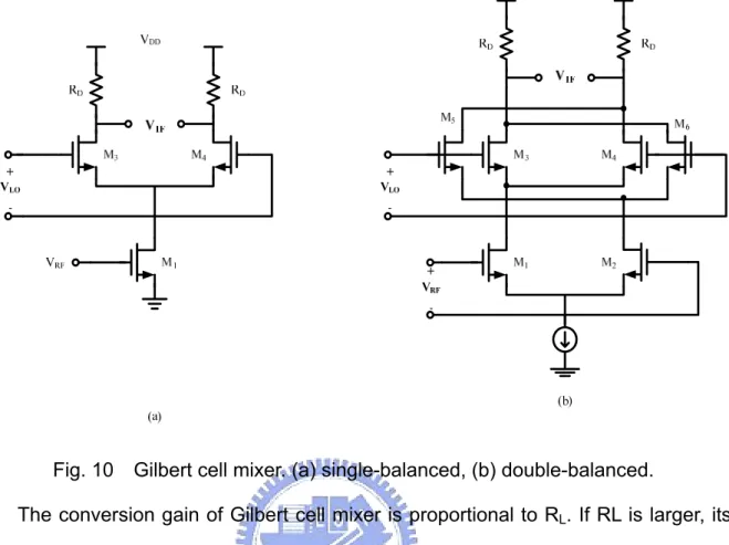
The purpose of the mixer is to convert a signal from one frequency to another. In a receiver path, this conversion is from radio frequency to intermediate frequency. Mixing requires a circuit with a nonlinear transfer function, since nonlinearity is fundamentally necessary to generate new frequencies. Therefore, if an RF input signal and a LO signal are passed through a system with second-order nonlinearity, the output signals will have components at the sum and difference frequencies. A circuit realizing such nonlinearity could be as a simple as a diode followed by some filter to remove unwanted signals. On the other hand, it could be more complex, such as the double-balanced cross-coupled circuit, commonly called the Gilbert cell. In this section, we will focus on CMOS Mixer.
The simple switch used as mixer is shown in Fig. 9. Fig. 9 shows that the output is equal to the RF input when S1 is on and zero when S1 is off. Note that the circuit is a
linear, time-variant system with respect to RF port and a nonlinear, time-variant system with respect to the LO port. The Fig. 9(b) incorporates a MOS switch to implement the Fig. 9(a). As the RF input signal varies, the gate-source overdrive voltage of M1 and hence its on-resistance change, introducing nonlinearity in the
Fig. 9 (a) A simple switch used as a mixer, (b) implementation of switch with a NMOS device.
The most popular mixer topology in the low-gigahertz range is the double-balanced cross-coupled circuit, Gilbert cell as shown in Fig. 10. The Gilbert cell consists of transconductance stage, differential switching pair and load. The transconductance stage generates current in proportional to RF signal. The differential switching pairs perform the chopping operation of the current output of the transconductance stage and thus down-convert the RF signal into the IF band. In order to drive differential pairs sufficiently to turn on and turn off, the LO signal strength should be large enough. If the LO signal is a square wave signal, the IF output current and conversion gain is found easily as the equation (2).
t V g t t V g IIF m RF RF LO sin LO ...) 2 m RFcos( RF LO) 3 1 )(sin 4 ( * sin 1 1 ω π ω + ω + ≈π ω −ω = (2)
Thus, the conversion gain is equal to 2/π*gm1RL.
The double-balance mixer shown in Fig. 10 (b) can eliminate the even-order distortion but its power consumption is also double.
Fig. 10 Gilbert cell mixer. (a) single-balanced, (b) double-balanced.
The conversion gain of Gilbert cell mixer is proportional to RL. If RL is larger, its
conversion gain would be larger with a larger voltage drop. Thus, the current-reuse bleeding mixer [9] bleeds the driver stage current with a current source, the current source being used as part of the driver stage. This topology would provide the better performance in terms of conversion gain, linearity, noise figure and LO isolation. The detailed schematic of current-reuse bleeding mixer is shown in Fig. 11.
Fig. 11 Schematic diagram of single-balanced mixer with current bleeding For high frequency mixer, the single-end transconductance mixer is very popular. All of the single-end transconductance mixer could approximately be divided into two portions shown in Fig. 12, gate-pumped and drain pumped mixer respectively.
Fig. 12 The simplified schematic of single-end transconductance mixers. (a) gate-pumped mixer. (b) drain-pumped mixer.
The gate-pumped mixer operates in the saturation region with Vgs close to the
threshold voltage Vth, where maximum nonlinearity variations of gm are achieved.
Since the LO power would apply with RF signal together and the LO and RF frequency are close for down conversion mixer, the LO to RF and RF to LO isolation are very poor. Typically, the single-gate mixer have one major practical implementation problem which requiring a hybrid power combining circuit to combine the LO and RF signals. Due to the high frequency operation, the hybrid can be easily integrated on-chip. The quadrature balanced mixer that consists of two unit single-end gate-pumped mixer and a 90o branch-line hybrid is shown in Fig. 1.
0
90
0
90
Fig. 13 Simplified circuit diagram of the single-gate quadrature balanced mixer [10]
For drain-pumped mixers, it’s LO power is fed at the drain of the transistor. Consequently, gm is a nonlinear function of Vds. The drain-pumped down-conversion
mixers have a significant advantage compared to the gate-pumped approach. The RF and LO frequency, which are close to together, are injected at different ports. Thus, the
simplifying the filtering circuit would improve the LO to RF and RF to LO isolation [11].
Fig. 14 Simplified circuit schematics of the passive drain-pumped resistive mixer [11]
In above discussion, the most of the CMOS RF mixers are realized by voltage or partial-voltage method. No current-mode approach is discussed for mixer design in high frequency domain. Therefore, a new approach of current-mode mixer is proposed in this thesis. The current-mode mixer is realized the down-conversion function with the multiplication between the RF and LO current signal. The operation method would be introduced in chapter 2 in detail.
1.3 Motivation
Early circuit design principles and techniques for current-mode processing, such as the translinear circuit principal introduced by Barrie Gilbert in 1972 is becoming powerful tools for the development of high performance analogue circuits and systems. The current conveyor is an extremely powerful analogue building block, combining voltage and current mode capability. In recent year, the current-mode circuits and sub-systems have a better performance in much application such as continuous-time and sampled-data filters, A/D and D/A converters, and current-mode neural networks. From above descriptions, we believe that current-mode system would also have the better performance in radio-frequency system. Thus, we would develop a new approach, current-mode operation, to design a 24GHz front-end circuit design with TSMC CMOS 0.13um technology.
1.4 Thesis
Organization
Chapter 2 proposes a new approach of current-mode receiver front-end, including the current-mode low-noise amplifier and current-mode mixer, and simulation results. Chapter 3 would illustrate the layout considerations, measurement considerations and setup and experimental results. Finally, the conclusions and future works are described in chapter 4.
CHAPTER 2
CIRCUIT DESIGN AND SIMULATION RESULTS
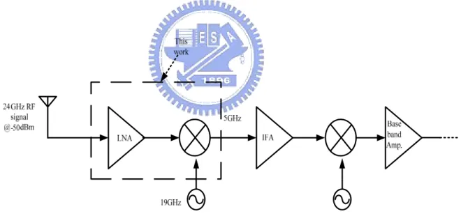
A new design approach, current-mode operation, will be proposed in this chapter. Using such approach, a low-noise amplifier and a down-conversion mixer are designed and implemented in TSMC 0.13um technology. This chapter is organized as following. In first two sections, the operational principles and design considerations of the current-mode LNA and mixer will be described in detail. Then, the post-simulation results would be illustrated in the last section. Fig. 15 shows the block diagram of the receiver front-end and the circuit blocks implemented in this work also are marked in this figure.
Fig. 15 Block diagram of the current-mode receiver front-end
The current-mode LNA consists of two stages and each is a current-mirror amplifier. The first stage uses a feedback inductor for input impedance and noise matching. The second stage is used to enhance the overall gain performance. The current-mode mixer consists both of I-sum and I-square circuit. The RF frequency is 24-GHz and 5-GHz is selected as the IF frequency.
2.1
Current-Mode Low-Noise Amplifier
Due to the leakage current of parasitic capacitance, the LNA must contain a single transistor before voltage amplification occurs [6]. Therefore, most of LNA in recent report above 20-GHz would use a single transistor as the first input stage [8][21][22][23]. However, all of them are realized by voltage-mode or partial-voltage mode operation. Therefore, a new approach of current-mode operation is proposed and performs a LNA. The current-mirror amplifier is also a single stage transistor, thus the current-mirror amplifier could also avoid the leakage current of parasitic capacitance. The 2-stage cascade current-mirror amplifiers are employed to implement a current-mode LNA.
2.1.1 Operational Principle and Design Consideration
The LNA amplifies the desired weakly RF signal received from an antenna while introducing a minimum amount of noise to the signal. Since the LNA is the first stage in the most receiver front-ends, its noise figure would directly add to the noise figure of the system and it must provide an input impedance matching for the maximum power transference.
The first stage of current-mode LNA is a current-mirror amplifier with a feedback inductor to improve the input matching and isolation. The second stage is also a current-mirror amplifier which is used to enhance the overall gain level. Thus, the current-mode LNA could be fed the desired RF current signal and generate a greater output current signal with a minimum amount of noise. And the output current signal of current-mode LNA can be injected into the current-mode down-conversion mixer directly.
2.1.1.1 Input Matching Network
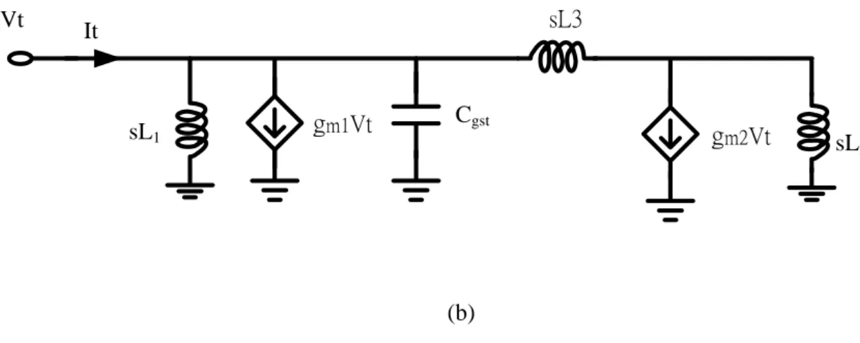
The first input stage of current-mode LNA is shown in the Fig. 16(a) and Fig. 16(b) is the small signal equivalent circuits. The value of inductor L1 is chosen to resonate
with the total capacitance seen at the drain terminal of M1. Therefore, the input current
signal can be fed into the transistor of M1 and use the current mirror pair of M1 and M2
to amplify the current signal. For the same reason, the value of inductor L2 is chosen to resonate with the total capacitance seen at the drain terminal of M2. Thus, the output current signal can be fed into next stage. The inductor L3 provides the shunt
feedback loop to improve the input impedance and isolation.
M1 M2 L1 L2 L3 VDD_LNA VDD_LNA C1 Rs Iin Zin Vout (a)
sL3
g
m2Vt It Vtg
m1Vt (b) sL2 Cgst sL1Fig. 16 Current-mirror amplifier with inductor feedback. (a) schematic (b) small signal equivalent circuits.
From Fig. 16(b), we could directly derive the value of input impedance of this stage. ) ( ) ( 1 1 1 2 2 1 3 2 2 3 1 3 2 2 3 L L C s L g L g L g s L L L sL sL I V Z gst m m m t t in + + + + + + + + = = (3) When1 2 ( 2 3) 0 1 3 2 + − + = + C L L L L L gst
ω , the above equation can be simplified to equation (4). 2 3 2 2 1 3 1 2 2 1 1 2 3 1 m m m m m in g L L L g L g L g L g L L Z + + = + + + = (4)
Because the size ratio between the transistor of M1 and M2 is chosen to decide
the ratio of current amplification, the suggestion is to choose the minimum size of transistor M1. Because the value of inductor L2 is chosen to resonate with total
capacitance seen at the drain terminal of M2, the inductor value of L2 is fixed.
Therefore, the value of input impedance can be modulated by change the value both of the transconductance of M2 and the value of inductor L3. But, the value of
transconductance gm2 is involved with the gain, noise figure and power consumption
performance. So, the choice of size value of transistor M2 needs to be considered in detail. Therefore, the value of inductor L3 is the most important key element to adjust
the input impedance. The feedback inductor is used to improve the isolation and input matching. Therefore, only one feedback inductor is needed to use in the first stage of current-mode LNA to provide input matching and fine isolation.
2.1.1.2 Noise and Linearity
Low noise figure, low power consumption, high linearity and high gain are the fundamental characteristic in LNA circuit design. But the noise figure, linearity and gain are trade-off with each other for the fixed power consumption. Hence, the optimum value of noise figure, gain and linearity can not be achieved at the same time.
Due to the cascade topology of current-mode LNA, it is significant to understand the effects of cascading on figure-of-merit, such as noise figure and linearity. It is known as Friis’s equation [12] that the noise figure of a cascade of signal blocks can easily be shown in the following equation.
) 1 ( 1 1 2 1 1 1 − − + + − + = m p p m p tot A A NF A NF NF NF … … (5)
where NFm is the noise figure of the mth stage evaluated with respect to the driving
the noise contributed by each stage decreases as the gain preceding the stage increases, implying that the first few stage in a cascade are most critical. Similarly, we could estimate the linearity of two stage current-mirror amplifier. The production if intermodulation distortion in each stage is complicated. With some simplifying assumption, we could obtain the following equation [2].
… + + + ≈ 2 3 , 3 2 2 2 1 2 2 , 3 2 1 2 1 , 3 2 3 1 1 IP p p IP p IP IP A A A A A A A (6)
Where AIP3,n denotes the input-referred third-order intercept point of the nth stage and
Apn is the power gain of the nth stage. According to the equation (5) and (6), the
trade-off between noise figure and linearity are involved with power gain. For example, the noise figure would reduce and linearity worse with a greater power gain. Therefore, the maximal power gain is not the best value. The design issue of the current-mode LNA is to achieve the lower noise figure and a greater power gain with a suitable linearity.
Since the noise figure in the first stage of current mode LNA would directly add to the system. Thus, the first stage of LNA would be performed with a low noise figure and greater gain. Then, the second stage would enhance the overall gain and achieve high linearity performance. However, the biasing voltage and transistor size would be involved with both of the power gain and noise figure performance. Therefore, the biasing voltage and transistor size need to choose carefully.
The noise contribution would be discussed in detail in the first instance. The dominant noise contribution brings from the MOS transistor. Therefore, the noise contribution of the CMOS device would be introduced clearly. The standard CMOS small signal noise model is shown in Fig. 17 [13] and the noise calculation would
adopt this noise model.
i
d 2i
g 2v
Rg 2Fig. 17 The standard CMOS small signal noise model [13].
The dominant noise source in the CMOS device is channel thermal noise. This source of noise is commonly modeled as a shunt current source in the output circuit of the device. The channel noise is white with a power spectral density given by
0 2 4 d d g kT f i γ = Δ (7) The parameter of gd0 is the zero-bias drain conductance of the device and γis a
bias-dependent factor that, for long-channel devices, satisfies the inequality 1
3 2 ≤γ ≤
(8) The value of 2/3 holds when the device is saturated and the value of 1 is valid when the drain-source voltage is zero. For short-channel devices, however, γ does not satisfy equation (8). In fact, γ can be much greater the 2/3 for short-channel devices operating in saturation [14].
This excess noise may be attributed to the presence of hot electrons in the channel. The high electric fields in sub-micron MOS devices cause the electron temperature, Te, to exceed the lattice temperature. The excess noise due to carrier
heating was anticipated by van der Ziel as early as 1970 [15].
Then, an additional source of noise in MOS devices is the noise generated by the distributed gate resistance [16]. This noise source could be modeled by a series resistance in the gate circuit and an accompanying white noise generator. By interdigitating the device, the contribution of this noise source could be reduced to insignificant levels. For noise purposes, the effective gate resistance is given by [17]
L n W R Rg 2 3 □ = (9) where R□ is the sheet resistance of the polysilicon, W is the total gate width of the
device, L is the gate length and n is the number of gate fingers used to layout the device. The factor of 1/3 arises from a distributed analysis of the gate, assuming that each gate finger is contacted only at one end. By contacting at both ends, this term reduces to 1/12. In addition, this expression neglects the interconnect resistance used to connect the multiple gate fingers together. Interconnect can be routed in a metal layer that possesses significantly lower sheet resistance and hence is easily rendered insignificant. Its significance is further reduced in silicided CMOS process which possess a greatly reduced sheet resistance, R□. Due to the TSMC CMOS 0.13um
technology which is a silicided CMOS process, the noise source of gate resistance would be neglected when calculating the noise contribution.
The gate-induced noise is proceeded to introduce. When the device is biased so that the channel is inverted, fluctuations in the channel charge would induce a physical current in the gate due to the capacitive coupling. At frequencies approaching ωT, the gate impedance of the device exhibits a significant phase shift from its purely
capacitive value at lower frequencies. This shift could be accounted by including a real conductance, gg, and a shunt noise current, i . Mathematical expressions for g2
g g g kT f i δ 4 2 = Δ (10) 0 2 2 5 d gs g g C g =ω (11) where δ is the coefficient of gate noise, classically equal to 4/3 for long-channel devices. The equations of (10) and (11) are valid when the device is operated in saturation. However, in the gate noise expression, gg is proportional to ω2 and hence
the gate noise is not a white noise source. Therefore, Fig. 18 is the simplified small signal noise model which neglected the Cgd capacitance for convenient estimation.
The Fig. 18 would apply to estimate the noise contribution of current-mode LNA.
i
d2
i
g2
Fig. 18 The simplified small signal noise model.
The noise performance of a circuit is usually characterized by a parameter called noise factor (F) or noise figure (NF ≡10logF) that represents how much the given
system degrades the signal-to-noise ratio [18].
out in
SNR SNR
only souece to due power noise output Total power noise output Total F = (13)
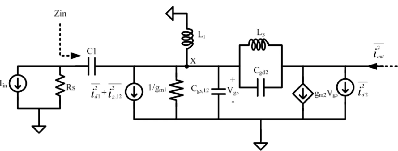
The simplified schematic diagram of noise source distribution of input stage is shown in Fig. 19. And the small signal equivalent circuit for noise calculation is shown in Fig. 20 where the channel thermal noise power of the mth MOS device is 2
,m n i equal to m do g kT ,
4 γ , the gated-induced noise power of the mth MOS device is ig2,m equal to
m d m gs g C , 0 2 , 2 5 ω
and the thermal noise power of Rs is 2
S R i equal to s R kT 4 . M1 M2 L1 L2 L3 VDD_LNA C1 2 Rs
i
Rs 2 1 , n i 2 2 , n i 2 12 , g ii
out 2 VDD_LNA X Zini
d 2 2i
i
d g 2 12 , 2 1+i
out 2Fig. 20 The small-signal circuit of input stage for noise calculations.
For noise calculation, the output noise power is estimated with some of the reasonable assumption. First, the inductor, L1, would resonate with the total parasitic capacitance at X node including the Cgs,12. Second, the inductor, L3, would resonate
with Cgd2. From the diagram of Fig. 20, the output noise power in2,out could be driven as following equation (14). 2 2 2 2 2 2 12 , 2 1 2 2 ,out ( R d g )*( s // in) * m d n i i i R Z g i i S + + + ≈ (14)
Due to the definition of equation (13), the noise factor of input stage of the current-mode LNA is presented as the following equation.
2 2 2 2 , 0 2 , 0 2 2 2 1 , 0 2 2 2 2 2 , * ) // ( * ) 5 ( 1 * ) // ( * m in s d s d gs d s m in s R out n g Z R g R g C g R g Z R i i NF S γ ω δ γ + + + ≈ = (15)
operating frequency and input impedance, Zin. However, the value of Cgs is
proportional to the size value of transistor. The biasing voltage would influence the value both of gd0 and Zin. In order to obtain the minimum noise figure, the optimum
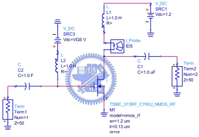
value both of transistor size and biasing voltage would be chosen with the simulator tools. The setup of NFmim versus VGS simulation is shown in Fig. 21.
TSMC_013RF_CYWU_NMOS_RF M1 nr=nr lr=0.13 um wr=1.2 um model=nmos_rf L L2 R= L=1.0 H L L1 R= L=1.0 H C C2 C=1.0 F V_DC SRC1 Vdc=1.2 C C1 C=1.0 uF Term Term2 Z=50 Num=2 I_Probe IDS V_DC SRC3 Vdc=VGS V Term Term1 Z=50 Num=1
Fig. 21 The setup of NFmin versus VGS simulation.
The parameter of nr is the finger number of transistor. The simulation results are shown in Fig. 22, the diagram of minimum noise figure versus biasing voltage, VGS,
with different transistor size. Then, the simulation result of the power gain, dB(S(2,1)), versus VGS with different transistor is shown in Fig. 23.
0.5 0.6 0.7 0.8 0.9 1.0 1.1
0.4
1.2
1.0
1.2
1.4
1.6
1.8
2.0
0.8
2.2
nr=8.00 nr=12.0 nr=16.0 nr=20.0 nr=24.0 nr=28.0 nr=32.0 nr=36.0 nr=40.0 nr=44.0 nr=48.0 nr=52.0 nr=56.0 nr=60.0 nr=64.0VGS
N
F
mi
n, dB
m2
m2
VGS=
NFmin[0]=1.280
nr=44.000000
650.0m
Fig. 22 The simulation result of minimum noise figure versus VGS.
0.5 0.6 0.7 0.8 0.9 1.0 1.1
0.4
1.2
-15
-10
-5
0
5
-20
10
nr=8.00 nr=12.0 nr=16.0 nr=20.0 nr=24.0 nr=28.0 nr=32.0 nr=36.0 nr=40.0 nr=44.0 nr=48.0 nr=52.0 nr=56.0 nr=60.0 nr=64.0VGS
dB
(S
21)
m1
m1
VGS=
dB(S21[0])=6.043
nr=44.000000
650.0m
From the simulation results, the noise figure would be worse with both of the larger transistor size and higher biasing voltage. But the power gain performance is greater with larger transistor size and biasing voltage. Thus, the minimum noise figure, power gain and power consumption are a trade-off. The design issue in this thesis is to achieve the lower noise figure with a suitable power gain and acceptable power consumption.
The linearity of the transistor is also involved with biasing voltage. Unfortunately, in the condition of the best noise figure performance is always the worst case of linearity performance. The Taylor series is used to expand the drain current. The drain current in Taylor expansions could be expressed as following:
… + + + + ≈ ' 2 " 3 ) ( ) ( GS DS GS m gs m gs m gs ds v I V g v g v g v i (16)
The third-order intercept point (AIP3) of gate voltage amplitude is shown as the
following equation. " 3 3 4 m m IP g g A = (17)
where gm is the transconductance of transistor and g"m is the second-order
differential of transconductance. And the simulation results about gm and g are m"
Fig. 24 The transconductance of transistor device.
From the simulation result of Fig. 24, the worst case of the third-order intercept point occurs at the biasing voltage of 550mV. But, the biasing voltage of 550mV is the best value of noise figure performance. From the simulation results of Fig. 22, Fig. 23 and Fig. 24, the value of biasing voltage is chosen as 650mV with a lower noise figure, suitable power gain, acceptable power consumption and linearity.
2.1.2
Circuit
Implementation
Fig. 25 shows the schematic of current-mode LNA in the receiver and Table(i) list the detailed parameters of each device. In the schematics, the MOS transistor pairs of M1,2 and M3,4 operate as the current-mirror amplifier. Due to the different power supply
voltage between LNA and Mixer, the MOS transistors of M5, M6 and M7 are the diode
connected MOS transistors employed to provide a suitable voltage drop for the same supply voltage in LNA and downconverter circuit. The inductors of L1, L2 and L3 would
respectively, to present high impedance for the RF signal. Also, the inductors of L1, L2
and L3 behave as DC current source. They provide the necessary DC bias current
without requiring extra voltage headroom. Besides, an additional advantage is to nullify the parasitic capacitances of the MOS transistors, resulting in an improvement of the noise figure [19]. The inductor of L4 is used to provide an inductor shunt
feedback to improve the isolation and the input matching. Therefore, only one feedback inductor is needed to use in the first stage of current-mode LNA to provide input matching and fine isolation. The capacitor of C1 and C2 are used as the block
capacitors at input and output terminals, respectively. The capacitor of C3 is used to
provide a stable AC ground.
Table(i) Detailed parameters of the current-mode LNA
M
1,3RF_MOS
1.2um*1/
0.13um
M
2RF_MOS
1.2um*44 / 0.13um
M
4RF_MOS
1.2um*26 / 0.13um
M
5RF_MOS
5.0um*30 / 0.13um
M
6,7RF_MOS
8.0um*30 / 0.13um
C
1Mmcap_um
9.0um*9.0um (89.4 fF )
C
2Mmcap_um
7.5um*7.5um (62.996 fF )
L
1Spiral_std rad= 15um w=9 nr=1.5 (297.81 pH )
L
2,3Spiral_std rad= 15um w=3 nr=1.5 (314.5 pH )
L
4Spiral_std rad= 32.5um w=3 nr=1.5 ( 506.7 pH)
2.2 Current-Mode Down-Conversion Mixer
The purpose of the mixer is to convert a signal from one frequency to another. In a receiver path, this conversion is from radio frequency to intermediate frequency. Frequency mixing requires a circuit with a nonlinear transfer function, since nonlinearity is fundamentally necessary to generate new frequencies. Therefore, if an RF input signal and a LO signal are passed through a system with second-order nonlinearity, the output signals will have components at the sum and difference frequencies. In the past research, most of the CMOS RF mixers are realized by voltage or partial-voltage method. No current-mode approach is discussed for mixer design in high frequency domain. Therefore, a novel aspect of current-mode mixer is proposed in this section.
2.2.1
Operational Principle and Design Consideration
Most of the high frequency CMOS mixers are realized the down-conversion function with the multiplications between RF and LO voltage signal. The Gilbert cell mixers and single-end transistor mixers are the most popular topologies. In this section, a new approach of current operation mixer is proposed. In opposite to the voltage mode or partial-voltage mode mixer, the current-mode mixer is realized the down-conversion function with the multiplication of the RF and LO current signal. Therefore, the I-sum and I-square circuits are necessary to perform the current-mode mixer. The I-Sum circuit would sum the current both of RF and LO ports and feed the output summing current into the I-square circuit to perform the current multiplication of RF and LO current signal. Fig. 26 shows the block diagram of current-mode mixer and the operation of circuit blocks in this work also are marked in this figure.
2.2.1.1 Current-summing circuit
For the operation of current mixing, the I-sum circuit is used to sum the RF and LO current signal. Then, the summing current both of the RF and LO port would be fed into the I-square circuit to perform the current multiplication as the down-conversion function. The current summing function is operated with two common-gate transistors connected the drain terminal together. Fig. 27 shows the I-sum circuit. The Ls1 and Ls2 resonate with the total parasitic capacitance seen at the
source of the transistor Ms1 and Ms2, respectively. The resonance would provide high
impedance. Therefore, the current signal both of the RF and LO port would be fed into common-gate transistors to perform the current summing operation. The inductor Ls3
resonates with the total parasitic capacitance seen at the output node of current summing circuit. For the same reason, the output current signal of I-sum circuit would be fed into the current squaring circuit to perform the operation of current multiplication.
2.2.1.2 I-square circuit
In this section, the I-square circuit would be discussed in detail. Fig. 28 is the simplified circuit of the current squaring.
Msq1 Msq2 Msq3 Iout + Va -+ Vb
-Iin V2 I3 I1 I2
Fig. 28 The simplified current squaring circuit.
Before the derivation of the current squaring function, some of the assumptions would be considered. First, the transistors of Msq1, Msq2 and Msq3 are operated in the
saturation region and all of threshold voltage is the same. Second, the value of k1(W/L)1 is equal to the value of k2(W/L)2 and k3(W/L)3. Thus, all of them are respected
as the symbol of K. The Iin is the ac signal of input current. From the Fig. 28, some of
the equality could be obtained easily.
1 3 I I Iin = − (18) 2 1 K(Va Vt) I = − (19)
2 3 K(Vb Vt) I = − (20) b a V V V2 = + (21)
From the above equation, the equation of Iin could be derived as following:
) )( 2 ( 2 1 3 t b a in I I K V V V V I = − = − − (22) ) 2 ( 2 t in a b V V K I V V − = − ⇒ (23)
Thus, the correlation between Va, Vb and Iin could be obtained. From the
correlation between equation (21) and (23), the value of Va and Vb could attain.
) 2 ( 2 2 2 2 t in b V V K I V V − + = (24) ) 2 ( 2 2 2 2 t in a V V K I V V − − = (25)
Intuitively, the summing current of I1 and I3 would have the current squared the
input current, Iin, 2 2 2 2 2 3 1 ) 2 ( 2 ) 2 ( 2 1 t in t V V K I V V K I I − + − = + (26)
Due to the current mirror pair of Msq1 and Msq2, the current I1 is similar with I2.
Therefore, the output current of the I-square circuit is equal to the current of I1+I3.
2 2 2 2 2 3 2 3 1 ) 2 ( 2 ) 2 ( 2 1 t in t out V V K I V V K I I I I I − + − = + = + = (27)
From the equation (27), some of the correlations would be obtained. The value of output current of current squaring circuit would be in reverse proportional to the value of V2-2Vt. For the same reason, the conversion gain of current mode down-conversion
mixer is in reverse proportional to the value of V2-2Vt. Due to the fixed value of Vt, the
conversion gain would be decided by the biasing voltage, V2. However, the
performance of linearity is proportional to the biasing voltage. Therefore, the performance of conversion gain and linearity are trade-off in the design consideration of I-square circuit. Fig. 29 presents the simulated results about conversion gain and linearity. From the simulated results, the optimal value of bias voltage V2 is about 1V.
0.4 0.6 0.8 1.0 1.2 1.4 1.6 -40 -30 -20 -10 0 10 -40 -30 -20 -10 0 10 P1 d B [ d B m ] C o n v e ri s on ga in [ d B] Bias voltage V2 [V] Conversion gain P1dB
Fig. 29 Conversion gain and 1dB compression point of current-mode downconverter
Due to the short-channel effect of MOS device, the drain current ID is shown as
following. ) 1 ( ) ( 2 1 DS m t GS ox n D V V V L W C I = μ − +λ ( 28)
The velocity saturation effect makes the drain current ID proportional to (VGS −VT)m
where 1≤ m<2. The drain current is correlated with VDS in the short-channel MOS
devices. For the different VDS voltage of VDS1 and VDS3, the function of current square circuit would be worsened. The equation of Iout is shown as (29) and all of the
detailed analysis would be introduced in the appendix I.
) 2 3 2 2 7 3 4 1 ( 4 ) 2 3 2 ( * ) 2 1 ( * ) 2V -K(V * ] * ) 4 1 ( * ) 2 3 2 ( 4 8 11 2 5 2 3 * ) 2 ( ) 4 1 ( ) 2 3 2 4 27 2 4 2 1 ( * ) 2 ( 2 [ )] 4 4 4 1 4 2 ( * ) 4 1 ( 1 1 [ * ) 2 ( 2 2 3 2 2 2 2 t 2 2 2 2 4 4 3 3 2 2 2 2 2 2 2 3 2 2 2 2 2 2 2 2 2 2 2 2 2 2 2 DD DD DD DD DD DD DD in DD DD DD DD DD DD DD t DD DD DD DD DD DD DD t DD DD DD DD DD DD DD t in out V V V V V V V I V V V V V V V V V V V V V V V V V V K V V V V V V V V V K I I λ λ λ λ λ λ λ λ λ λ λ λ λ λ λ λ λ λ λ λ λ λ λ λ λ λ λ λ λ λ λ λ λ λ + Δ + Δ + Δ + + + + Δ + + + Δ + + + + + + − − + + + Δ + Δ − Δ − + + − + Δ + − − + + Δ + Δ + + + − = (29) )} 4 1 4 2 ( ] 4 * ) 1 [( * ) 4 1 ( 1 1 { * ) 2 ( 2 2 2 2 2 2 2 2 2 DD DD DD DD DD DD DD t in out V V V V V V V V V K I I
λ
λ
λ
λ
λ
λ
λ
λ
+ + Δ + Δ − + + + − − ∝ ⇒ ) 4 1 4 2 ( ] 4 * ) 1 [( * ) 4 1 ( 1 ) 1 ( ) 2 ( 2 2 2 2 2 2 2 2 2 DD DD DD DD DD DD DD t in V V V V V V V where V V K I λ λ λ λ λ λ λ λ δ δ + + Δ + Δ − + + + = − − = ( 30)Thus, the smaller difference between VDS1 and VDS3 is the better for the current square
operation. The following figure represents the impact of difference VDS voltage. The
smaller difference of VDS voltage will have the greater conversion gain of
current-mode mixer. Therefore, there are two important issues about the current square circuit. First, the channel length of MOS devices in the current square circuit should be chosen as larger channel length to alleviate the short channel effect. Second, the biasing voltage of current square circuit should be chosen with the smallest difference of VDS between M1 and M3 MOS devices. While the V2 is equal to
VDD, the voltage of VDS1 is very close to VDS3.
0.9 1.0 1.1 1.2 1.3 1.4 1.5 -8 -6 -4 -2 0 2 4 6 0.00 0.05 0.10 0.15 0.20 0.25 0.30 0.35 Di ffe re
nce between VDS1 and VDS3 [V
] Conv ersi on gai n [ d B ]
Biasing voltage V2 of current square circuit [V]
Conversion gain |VDS1-VDS3|
Fig. 30 The impact of difference of VDS voltage
The drain current ID of MOS devices may not a quadratic equation of VGS. Fig. 31
compares the difference of drain current between the modified quadratic equation of VGS-Vt and model definition. Below the bias voltage of 0.8V, the differences are very
slight. The operated voltage of MOS device in the current squaring circuit is below 0.8V. Therefore, the drain current equation is closed to the quadratic equation of VGS.
The functionality of current squaring is acceptable.
Fig. 31 The difference of drain current of between the modified quadratic equation of VGS-Vt and model definition.
While the input current of I-square circuit is the summing current between ILO and
IRF, the output current of I-square circuit could obtain the mixing frequency between
ωRF and ωLO. Therefore, the operation of down-conversion mixing can be
Fig. 32 The complete whole circuit of I-square circuit.
The capacitance of Csq1 is the block capacitance between I-sum and I-square
circuit. The inductor of Lsq1 resonates with the capacitance of Csq2 at the intermediate
frequency of 5-GHz and provide high impedances at output terminal of I-square circuit. Therefore, the Lsq1 and Csq2 could be used as the filter to percolate the leakage signal
of LO frequency (19-GHz), RF frequency (24-GHz), up-conversion frequency (19-GHz+24-GHz), the double frequency of RF and LO frequency (48-GHz and 38-GHz) and third frequency of RF and LO frequency (72-GHz and 57-GHz).
2.2.2
Circuit
Implementation
The complete schematic of current-mode mixer is shown in Fig. 33 and Table(ii) lists the detailed parameters of each device. The current-mode mixer is composed of three blocks, the I-sum circuit, I-square circuit and output current buffer. First, the I-sum circuit consists of transistors, Ms1 and Ms2, and the inductors, Ls1, Ls2 and Ls3.
The transistors of Ms1 and Ms2 are the common-gate topology connected the drain
terminal together. The inductor of Ls1 and Ls2 resonate with the total parasitic
capacitance seen at source node of Ms1 and Ms2, respectively. Thus, the LC
resonance would provide the high impedance to feed the RF and LO current signal into the common-gate transistor connected the drain terminal together. Then, the inductor Ls3 resonates with the total parasitic capacitance seen at the output node of
current summing circuit. Thus, the resonation of Ls3 would provide high impedance to
feed the output current of summing circuit into the current squaring circuit. Second, the I-square circuit is composed of transistor of Msq1, Msq2 and Msq3, capacitance of
Csq1 and Csq2, and the inductor of Lsq1. The transistor of Msq1, Msq2 and Msq3 would
perform the operation of current squaring. The inductor resonates with Csq2 at intermediate frequency of 5-GHz. The resonation between Lsq1 and Csq2 would
provide high impedance to feed the output current of current squaring into output current buffer. Finally, the output current buffer provided the performance of 0-dB consists of the transistor of Mb1, Mb2 and inductor, Lb1. Table(ii) lists the detailed
parameters of current-mode downconverter.
Fig. 33 The complete circuit of the current-mode circuit. Table(ii) Detailed parameters of current-mod downconverter.
M
s1,2RF_MOS
1.2um*32 / 0.13um
M
sq1,2,3RF_MOS
1.2um*12 / 0.13um
M
b1RF_MOS
1.2um*1 / 0.13um
M
b2RF_MOS
5.0um*30 / 0.13um
C
s1Mmcap_um
7.5um*7.5um (62.996 fF )
C
s2Mmcap_um
16um*16um (273.95 fF )
C
sq1Mmcap_um
11um*11um (131.881 fF )
C
sq2Mmcap_um
31um*31um (1.0 pF)
C
b1Mmcap_um
23.5um*23.5um (583.4 fF )
L
s1Spiral_std rad= 20um w=3 nr=3.25 (945.25 pH )
L
s2Spiral_std rad= 26um w=3 nr=2.75 (916.56 pH )
L
s3Spiral_std rad= 27.0um w=3 nr=1.5 (443.21 pH )
L
sq1Spiral_std rad= 15.5um w=3 nr=3.5 ( 884.52 pH)
2.3 Simulation Results
The post-simulation is completed by ADS simulator for whole simulation with process parameters of TSMC 0.13-um CMOS MS/RF general purpose 1P8M salicide Cu-FSG 1.2V/2.5V RF SPICE models. The following diagrams are the post-simulation results of thorough receiver circuits.
LNA
Because the first stage of receiver is LNA, it must provide input matching, power gain and low-noise contribution in a specific frequency band. The figures from Fig. 34 to Fig. 37 are the port-simulation results of S-parameters, S11, S22, S21 and S12, respectively. The input and output matching are lower than -10dB indicated a power transfer greater than 90%. Fig. 38 exhibits that the noise figure is lower 3.5dB at the frequency of 24-GHz. The resultant noise figure is close to the minimum noise figure. The simulation results of linearity are shown in Fig. 39, Fig. 40 and Fig. 41. The linearity performance of input 1-dB compression (P1dB) is about -21.3dBm. The input
third-intercept point (IIP3) is about -11.7dBm. The transient simulation results of input and output current amplitude are shown in Fig. 42. The stability simulation results of stability factor and stability measure are shown in Fig. 43 and Fig. 44. The necessary and sufficient conditions for unconditional stability are that the stability factor is greater then unit and the stability measure are positive. The Table(iii) is the comparison with previously reported LNA for frequencies around 20-GHz. The conversion gain of current-mode LNA is dominant with the device size ratio of current-mirror amplifier. Thus, the supply voltage has slight effect on the conversion gain. But the supply voltage would have great effects on the power consumption.
20 22 24 26 28 18 30 -10 -8 -6 -4 -12 -2
freq, GHz
dB
(S
(1,
1))
m3
m3
freq=
dB(S(1,1))=-10.526
24.00GHz
Fig. 34 Simulation result S11 of LNA.
20 22 24 26 28 18 30 -30 -20 -10 -40 0
freq, GHz
dB
(S
(2,
2))
m4
m4
freq=
dB(S(2,2))=-24.477
24.00GHz
20 22 24 26 28 18 30 5 10 15 0 20
freq, GHz
dB
(S
(2
,1
))
m5
m5
freq=
dB(S(2,1))=17.117
24.00GHz
Fig. 36 Simulation result S21 of LNA.
20 22 24 26 28 18 30 -45 -40 -35 -50 -30
freq, GHz
dB
(S
(1,
2))
m8
m8
freq=
dB(S(1,2))=-46.130
24.00GHz
20 22 24 26 28 18 30 4 5 6 7 3 8
freq, GHz
nf
(2)
m6
NF
m
in
m7
m6
freq=
nf(2)=3.447
24.00GHz
m7
freq=
NFmin=3.391
24.00GHz
Fig. 38 Simulation result NFmin of LNA.
-35 -30 -25 -20 -15 -10 -5 -40 0 -20 -10 0 10 -30 20 RF_pwr dB m (H B 1. H B .V o_ LN A [::,1 ]) m1 P1 dB m2 m1 RF_pwr= dBm(HB1.HB.Vo_LNA[::,1])=-22.875-40.000 m2 RF_pwr= P1dB=-5.175-21.300
-35 -30 -25 -20 -15 -10 -5 -40 0 0 5 10 15 -5 20
RF_pwr
C
onv
ers
ion_gai
n
m11
m12
m11
RF_pwr=
Conversion_gain=17.125
-40.000
m12
RF_pwr=
Conversion_gain=16.114
-21.300
Fig. 40 Simulation result of conversion gain of LNA.
-40 -30 -20 -10 -50 0 -100 -50 0 -150 50 RF_pwr dB m (m ix (H B .V o_LN A ,{ 2, -1} )) m2 dB m (m ix (H B .V o_ LN A ,{ 1, 0} )) m1 fir st _hor m onic th ird_hor m onic m2 RF_pwr= dBm(mix(HB.Vo_LNA,{2,-1}))=-109.527-50.000 m1 RF_pwr= dBm(mix(HB.Vo_LNA,{1,0}))=-32.948-50.000 RF_pwr -50.000 IIP3 -11.711
0.2 0.4 0.6 0.8 1.0 1.2 1.4 1.6 1.8 0.0 2.0 -100 0 100 -200 200 time, nsec TR A N .I _LN A out .i, uA
m3
TR A N .I _LN A in. i, uAm7
m3
time=
TRAN.I_LNAout.i=162.0uA
620.4psec
m7
time=
TRAN.I_LNAin.i=25.84uA
615.2psec
Fig. 42 Transient simulation result of LNA.
Eqn
K=stab_fact(S)
20 22 24 26 28 18 30 4 6 8 10 12 2 14freq, GHz
K
Fig. 43 Simulation result K-factor of LNA. 20 22 24 26 28 18 30 0.4 0.6 0.8 1.0 1.2 0.2 1.4
freq, GHz
b
Eqn
b = stab_meas(S)
Fig. 44 Simulation result stability measure of LNA.
0.4 0.5 0.6 0.7 0.8 0.9 1.0 1.1 1.2 1.3 0 10 20 30 40 50 60 0 10 20 30 40 50 60 P ow e r c on s um pt ion [ m W ] S21 [ d B]
Supply voltage of current-mode LNA [V]
S21
power consumption
![Fig. 3 Common-gate amplifier used a cascode transistor in the LNA [4] .](https://thumb-ap.123doks.com/thumbv2/9libinfo/7493583.115583/15.892.270.677.288.701/fig-common-gate-amplifier-used-cascode-transistor-lna.webp)
![Fig. 5 The high frequency effect of the cascode LNA topology [6].](https://thumb-ap.123doks.com/thumbv2/9libinfo/7493583.115583/16.892.130.796.526.1098/fig-high-frequency-effect-cascode-lna-topology.webp)
![Fig. 13 Simplified circuit diagram of the single-gate quadrature balanced mixer [10]](https://thumb-ap.123doks.com/thumbv2/9libinfo/7493583.115583/24.892.143.792.491.893/fig-simplified-circuit-diagram-single-quadrature-balanced-mixer.webp)
![Fig. 14 Simplified circuit schematics of the passive drain-pumped resistive mixer [11]](https://thumb-ap.123doks.com/thumbv2/9libinfo/7493583.115583/25.892.180.751.206.716/simplified-circuit-schematics-passive-drain-pumped-resistive-mixer.webp)