S- plus C-band erbium-doped fiber amplifier
in parallel structure
Chien-Hung Yeh
*, Chien-Chung Lee, Sien Chi
1Institute of Electro-Optical Engineering, National Chiao Tung University, 1001 Ta-Hsueh Road, Hsinchu 30050, Taiwan, ROC Received 18 December 2003; received in revised form 25 May 2004; accepted 7 July 2004
Abstract
A new S- plus C-band erbium-doped fiber amplifier (EDFA) module with coupled structure over 96 nm gain band-width of 1480–1576 nm has been experimentally investigated and demonstrated. For this proposed configuration, 30 and 36.2 dB peak gains are observed at 1506 and 1532 nm, respectively, when the input signal power is 25 dBm. In addition, this proposed amplifier module also can provide a broadband amplified spontaneous emission (ASE) light source from 1480 to 1572 nm.
Ó 2004 Elsevier B.V. All rights reserved.
PACS: 42.65.Y
Keywords: EDFA; Wideband; Coupled structure; WDM systems; S-band
1. Introduction
Wide-band erbium-doped fiber amplifiers (ED-FAs) are considerably expected and interested for high-capacity in dense wavelength division multiplexing (DWDM) systems. However, the transmission capacities in DWDM systems were limited by the gain bandwidth of the conventional
C-band erbium-doped fibers (EDFs) between 1530 and 1560 nm. Furthermore, the L-band (1560– 1610 nm) fiber amplifier techniques have been achieved, such as the EDFAs by using a longer
EDF than that of C-band EDFAs[1], the fiber
Ra-man amplifiers[2], and the different hybrid
ampli-fiers[3]. In addition, a wideband EDFA from C- to
L-band by employing coupled structure has also
studied [4]. Recently, an new S-band (1450–1530
nm) amplification technique, which utilizes er-bium-doped silica fiber with depressed cladding design and 980 nm pump laser to generate
EDF gain extension effects, has been reported [5].
0030-4018/$ - see front matter Ó 2004 Elsevier B.V. All rights reserved.
doi:10.1016/j.optcom.2004.07.018
*
Corresponding author. Tel.: +886-3-5712121x52998/939-442785; fax: +886-3-5716631.
E-mail address:[email protected](C.-H. Yeh).
1 Fellow, OSA.
Therefore, by employing a coupled structure and the new S-band amplifier module can retrieve the wide gain bandwidth from S- plus C-band. In this paper, we have proposed and experimentally dem-onstrated a coupled structure and S- plus C-band EDFA module with 96 nm gain bandwidth of 1480–1576 nm. In addition, the performance of this proposed EDFA module has also been studied.
2. Experiments and discussions
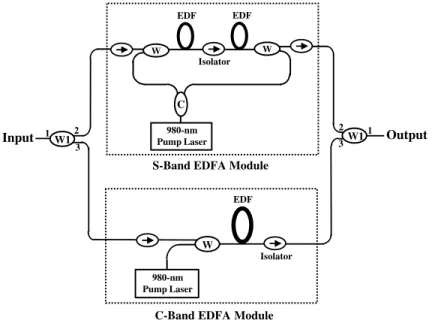
Fig. 1 shows the experimental setup for the wideband EDFA module from S- to C-bands by using a coupled structure. This configuration is constructed by two 1480/1550 nm WDM couplers
(W1), an S-band EDFA module composed of two
EDFA stages and a power-sharing 980 nm pump laser, and a conventional C-band EDFA module. Two WDM couples were used to connect two EDFA modules in parallel, and the output ranges of the port ‘‘1’’, ‘‘2’’ and ‘‘3’’ were 1480–1600, 1480–1520 and 1520–1600 nm, respectively, as
seen in Fig. 1. The S-band EDF inside EDFA
module has a depressed cladding design in order to provide a sharp, high attenuation, long
wave-length cutoff filter into active fibers. Then, the composition of the core is approximately 2.5%
GeO2, 5.5% Al2O3 and 92% SiO2, with 0.15 wt%
Erbium. The depressed cladding is approximately
3% Fluorine, 0.5% P2O5and 96.5% SiO2. The
nu-merical aperture of the core, relative to the de-pressed cladding, is 0.22. The S-band EDF inside EDFA module has a depressed cladding design in order to provide a sharp, high attenuation, long wavelength cutoff filter in the EDF. The cutoff wavelength is near at 1530 nm. The fabrication uses standard MCVD processes and solution doping for incorporation of aluminum and erbium. The core and cladding diameters are 4 and 22 lm, respectively. The numerical aperture of the core, relative to the depressed cladding, is 0.22. The
background loss is less than 5 dB km 1. This
S-band EDFA was fusion direct spliced to SMF-28 using standard setting. Typical splice losses were 0.5 dB. The EDFs in the first and second stages have different characteristics. The fiber in the first stage has the fiber length of 20 m, and can provide low noise figure and medium gain by forward pumping. The fiber in the second stage has the fi-ber length of 30 m, and can produce large output power by backward pumping. In addition, the op-tical isolator between these two stages can reduce
980-nm Pump Laser EDF W W1 Pump Laser980-nm W1 W EDF EDF W Isolator C
C-Band EDFA Module S-Band EDFA Module
Input Output
Isolator
1
1 2 2
3 3
backward amplified spontaneous emission (ASE) and improve noise figure performance. The total pump power of this amplifier module can be up to 280 mW while the bias current is operated at 356 mA. Furthermore, the evolution from a stand-ard EDFA to this S-band design by the introduc-tion of a continuous long wavelength cutoff filter in the EDF. Although the spectrum indicates strong gain at S-band wavelengths, the gain can-not be realized because of strong ASE at the 1530 nm peak, which limits the length of the pop-ulation inversion. Introduction of a progressively sharper long wavelength cutoff filter suppresses the gain in the C- and L-bands, so that the S-band region can exhibit increasing gain, as ASE from the 1530 nm peak does not grow and limit the pop-ulation inversion. Final result is a complete sup-pression of the longer wavelength gain, resulting in a usable high net gain in the S-band. However, the C-band EDFA module composed of a 980 nm pump power of 140 mW, a 980/1550 nm WDM coupler, a EDF (HighWave-742) length of 10 m long and two optical isolators.
To ensure the performances for this proposed
amplifier module inFig. 1, the input signal power
Pin = 5, 15 and 25 dBm are used to probe
the gain and noise figure spectra, respectively. Fig. 2shows the gain and noise figure spectra for
the S-band EDFA module ofFig. 1. The inset of
Fig. 2 also shows the ASE spectrum with 40 nm bandwidth of 1480–1520 nm for the S-band ampli-fier module. The gain and noise figure of the S-band EDFA can reach 34.1 and 6.8 dB at 1506 nm when
the input signal power is 25 dBm as shown inFig.
2. It also shows the gain of >10 dB and the noise fig-ure of 6.7–13.5 dB over the wavelength of 1480–
1520 nm with 5 dBm input signal power.Fig. 3
shows the gain and noise figure spectra from 1520
to 1580 nm for the C-band EDFA module of Fig.
1. As the same above operation conditions, 38.6
dB peak gain and 5.4 dB noise figure can be ob-tained, and the gain of >12 dB and the noise figure of <5.8 dB over the wavelengths of 1520–1580 nm
are observed inFig. 3.Figs. 4(a) and (b) indicate
the gain and noise figure spectra of the proposed
wideband EDFA module inFig. 1while the input
signal power Pin = 5, 15 and 25 dBm,
respec-tively. The inset of Fig. 4(a)shows the ASE
spec-trum over 98 nm bandwidth of 1480–1572 nm for this proposed structure as the optical output power
level above 40 dBm. Besides, the inset ofFig. 4(b)
presents that the insertion loss spectra of port ‘‘2’’ and ‘‘3’’ for two 1480/1550 nm WDM couplers, and two loss curves fold downward at around
1522 nm. Fig. 4(a) represents the gain of >10 dB
over 96 nm gain bandwidth of 1480–1576 nm while the input signal power of < 5 dBm. Due to the in-sertion loss of two WDM couplers, the different gain spectra of this proposed amplifier is smaller
Wavelength (nm) 1470 1490 1510 1530 Gain (dB) 0 10 20 30 40 50 Noise Figure (dB) 0 10 20 30 40 50 G: Pin = -5dBm G: Pin = -15dBm G: Pin = -25dBm NF: Pin = -5dBm NF: Pin = -15dBm NF: Pin = -25dBm S-Band ASE Wavelength (nm) 1470 1500 1530 Power Level (dBm) -45 -30 -15
Fig. 2. The gain and noise figure spectra for the S-band EDFA
module while the input signal powers Pin = 5, 15, and 25
dBm, respectively. The inset of this figure is ASE spectrum of the S-band amplifier module.
Wavelength (nm) 1510 1530 1550 1570 1590 Gain (dB) 0 10 20 30 40 50 Noise Figure (dB) 0 5 10 15 20 G: Pin = -5dBm G: Pin = -15dBm G: Pin = -25dBm NF: Pin = -5dBm NF: Pin = -15dBm NF: Pin = -25dBm
Fig. 3. The gain and noise figure spectra of the C-band EDFA
module while the input signal power Pin = 5, 15 and 25
than that of the S- and C-band amplifier individu-ally, and the gain spectra drops at near 1522 nm,
as seen inFig. 4(a). Compared with mentioned
S-and C-bS-and EDFA individually, the noise figure al-so degraded above 0.7–1.3 dB (especially between 1516 and 1524 nm) from 1480 to 1576 nm as shown inFig. 4(b). In addition, 30 dB peak gain with 8.2 dB noise figure, and 36.2 dB peak gain with 7.3 dB noise figure can be observed at 1506 and 1532 nm, respectively, while the input signal power of 25 dBm. However, the insertion loss ofthe band-pass coupler seem a little high in the 1520 nm range and the consequent amplifier noise figure in that re-gion is well over 10 dB for all input conditions for the wavelengths from 1510 to 1526 nm as shown
inFig. 4(b). According toFig. 4, the gain and noise figure spectra also show the behavior and perform-ance of that when three different input signal power
levels (Pin = 5, 15 and 25 dBm) are applied in
the experiment, respectively. Therefore, the pro-posed EDFA can be used to act as the in-line, pre- or post-amplifier in the optical WDM systems. Compared with the past broadband amplifier
tech-niques[6,7], which used thulium-doped fiber type
or Raman amplification, the proposed amplifier employs two EDF amplifier modules in parallel configuration over the gain bandwidth from 1480 to 1576 nm. The proposed EDFA has the advan-tage of wide bandwidth, potentially lower cost and simple architecture.
As a result, this proposed amplifier module based on coupled structure could achieve 96 nm gain bandwidth of 1480–1576 nm and the gain of >10 dB has been reached simultaneously when the input signal power level of < 5 dBm. Besides, this proposed amplifier module also provides a broadband ASE light source from1480 to 1572 nm. Therefore, this proposed EDFA module may be used in WDM networks.
3. Conclusion
In summary, we have experimentally investigated and demonstrated a new S- plus C-bands EDFA module in parallel structure over 96 nm gain band-width of 1480–1576 nm when the gain of >10 dB
(the input signal power level could great than 5
dBm) over the bandwidth of 1480–1576 nm. For the proposed EDFA, 30 dB peak gain with 8.2 dB noise figure and 36.2 dB peak gain with 7.2 dB noise figure can be observed at 1506 and 1532 nm, respectively, while the input signal power of 25 dBm. In addition, this proposed amplifier module also can provide a broadband ASE light source from 1480 to 1578 nm while the optical
out-put level above 40 dBm.
Acknowledgements
The authors thank C.Y. Chen for help with the experiment. Wavelength (nm) 1470 1490 1510 1530 1550 1570 1590 Gain (dB) 0 10 20 30 40 50 60 70 Pin = -5 dBm Pin = -15 dBm Pin = -25 dBm ASE Spectrum Wavelength (nm) 1470 1500 1530 1560 1590 Power Level (dBm)-45 -25 -5 Wavelength (nm) 1470 1490 1510 1530 1550 1570 1590 Noise Figure (dB) 0 5 10 15 20 25 30 Pin = -5 dBm Pin = -15 dBm Pin = -25 dBm Wavelength (nm) 1470 1500 1530 1560 1590 Insertion Loss (dB) -2 2 6 10 14 Port 2 Port 3 (a) (b)
Fig. 4. (a) The gain and (b) noise figure spectra of the proposed
configuration inFig. 1while the input signal powers Pin = 5,
15 and 25 dBm, respectively. The inset of (a) and (b) are the
ASE spectrum of the proposed structure and the insertion loss of 1480/1550 nm WDM coupler versus operating wavelength, respectively.
References
[1] Y. Sun, J.W. Sulhoff, A.K. Srivasta, J.L. Zyskind, T.A. Strasser, J.R. Pedrazzani, C. Wolf, J. Zhou, J.B. Judkins, R.P. Espindola, A.M. Vengsarkar, Electron. Lett. 33 (23) (1997) 1965. [2] S. Namiki, Y. Emori, IEEE J. Sel. Top. Quantum Electron.
7 (1) (2001) 3.
[3] H. Masuda, S. Kawai, IEEE Photon. Technol. Lett. 11 (1999) 647.
[4] B. Min, H. Yoon, W.J. Lee, N. Park, IEEE Photon. Technol. Lett. 12 (2000) 480.
[5] M.A. Arbore, Y. Zhou, G. Keaton, T.J. Kane, in: Proc. of the SPIE, Optical Devices for Fiber Communication IV, vol. 4989, 2003, p. 47.
[6] K. Fukuchi, et al., in: OFCÕ2001, 2001, PD24.
[7] N.E. Jolley, et al., in: Conference of Optical
Ampli-fiers and Their AmplicationsÕ 98, TuD2, 1998, p.