低功率循序串列於繞線端最佳化方法研究
49
0
0
全文
(2) 低功率循序串列於繞線端最佳化方法研究 Simultaneous Power and Routing Cost Minimization in Scan Chain Design. 研 究 生:許力中. Student:Li-Chung Hsu. 指導教授:陳宏明. Advisor:Hung-Ming Chen. 國 立 交 通 大 學 電子工程系 碩 士 論 文. A Thesis Submitted to Department of Electronics Engineering & Institute of Electronics College of Electrical Engineering and Computer Science National Chiao Tung University in partial Fulfillment of the Requirements for the Degree of Master in Electronics Engineering June 2005 Hsinchu, Taiwan, Republic of China. 中華民國九十四年六月.
(3) 低功率循序串列於繞線端最佳化方法研究 學生: 許力中. 指導教授: 陳宏明. 國立交通大學 電子工程學系 電子研究所 碩士班. 摘. 要. 隨著深次微米超大型積體電路製造技術的的進步,我們可以將系統整合到 單晶片上。 由於系統單晶片的複雜度極高,測試電路在設計上也因而遇到 許多挑戰。在所有測試電路的設計技巧上,嵌入式掃描串列(scan-based built-in-seft-test)架構在工業界上最被普遍應用。然而,當掃描串列沒有良好 的佈局或順序時,他們在電路測試階段將比正常工作時消耗更多的功率。 這些多出來的功率消耗將可能導致晶片製造良率下降及突然的電路損害。 在這篇論文,我們將提出一個有效的方法來同時降低測試功率消耗及降低 掃描串列所造成的繞線成本。由實驗結果可以得知我們的方法跟之前的利 用分割電路方法的論文 [6] 做比較的話,在相同的繞線成本下,最多可以 減少至少百分之十以上的測試功率消耗。. i.
(4) Simultaneous Power and Routing Cost Minimization in Scan Chain Design Student: Li-Chung Hsu. Advisor: Hung-Ming Chen. Department of Electronics Engineering Institute of Electronic Engineering National Chiao Tung University. ABSTRACT With advanced VLSI manufacturing technology in deep submicron (DSM) environment, we can integrate entire electronic systems on a single chip (SoC). Due to the complexity in SoC design, circuit testability becomes one of the most challenging work. Among design for testability (DFT) techniques, scan-based built-in self-test (BIST) architectures are widely used in industry. However, without careful design in scan cell placement and chain ordering, circuits consume much more power in test mode operation than that in normal functional mode. This elevated testing power may cause problems including overall yield lost and instant circuit damage. In this thesis, we present an effective approach to simultaneously minimizing test power and routing cost in scan chain design after cell placement. The experimental results are encouraging. Compared with a recent result in [6], which uses the approach with clustering overhead, we obtain up to 10% power saving under the same routing cost.. ii.
(5) 誌. 謝. 不能免俗的,在這邊我要感謝幫我完成這篇論文的貴人。首先,我要感 謝我的論文指導教授陳宏明博士,因為老師的熱心的指導與協助,能讓我 在嘗試極少錯誤下順利完成論文研究,並在論文寫作上及研究方法上,得 到獲益良多的智識,並感謝口試指導委員李毅郎教授、江蕙如教授、劉靖 家教授的親臨指導,由於教授的參與,讓學生對於所作的研究有更進一步 的啟發。 其次,我要感謝我的家人,能給予我衣食無缺的生活,在無經濟壓力 的生活下能專注於學術研究。 我要感謝我各實驗室的大學同學及實驗室同學,給予我在課業上及生活 上的鼓勵與幫助。.
(6) Simultaneous Power and Routing Cost Minimization in Scan Chain Design Prepared by Li-Chung Hsu Directed by Prof. Hung-Ming Chen. In Partial Fulfillment of the Requirements for the Degree of Master of Science. Department of Electronics Engineering National Chiao Tung University Hsinchu, Taiwan 300, R.O.C. E-mail: [email protected].
(7) Contents. 1 Introduction. 1. 1.1. Motivation of Reducing Scan Test Power . . . . . . . . . . . . . . . .. 2. 1.2. Organization of The Thesis. 4. . . . . . . . . . . . . . . . . . . . . . . .. 2 Low Power Scan Chain Design. 5. 2.1. Scan Based Test . . . . . . . . . . . . . . . . . . . . . . . . . . . . . .. 5. 2.2. Power Driven Scan Chain Reordering . . . . . . . . . . . . . . . . . .. 7. 2.3. Routing Constrained Low Power Scan Chains . . . . . . . . . . . . .. 8. 3 Low Power Scan Chain Optimization During Detailed Placement and Post Placement Phase 3.1. 13. Optimizing Low Power Scan Chain during Detailed Placement Procedure . . . . . . . . . . . . . . . . . . . . . . . . . . . . . . . . . . . 14. 3.2. Optimizing Low Power Scan Chain during Post Placement Phase . . 16. 4 Scan Chain Reordering with Power and Routing Cost Minimization. 18. 4.1. Weighted Graph Construction Using Power and Routing Cost . . . . 19. 4.2. Efficient Heuristic in Finding Minimum Cost Scan Chain Order . . . 19. iii.
(8) 4.3. Power Estimation for Scan-in and Scan-out Ports Determination . . . 20. 5 Experimental Results 5.1. 23. Detailed Placement with Minimizing Wirelength of Low Power Scan Chain . . . . . . . . . . . . . . . . . . . . . . . . . . . . . . . . . . . 24. 5.2. Optimizing Low Power Scan Chain during Post Placement Phase . . 26. 5.3. Scan Chain Reordering with Power and Routing Cost Minimization . 26. 6 Conclusion and Future Work. 32. iv.
(9) List of Figures 2.1. Application of tests via scan . . . . . . . . . . . . . . . . . . . . . . .. 2.2. Cell-based VLSI design flow with DFT. Scan chain reordering is performed after placement. . . . . . . . . . . . . . . . . . . . . . . . . .. 2.3. 6. 7. (A) Example set of scan-in vectors and output response. (B)Complete weighted graph. Nodes represent scan cell and edges represent connection between nodes. The edge weight is bit difference between two scan cells. . . . . . . . . . . . . . . . . . . . . . . . . . . . . . . . . .. 2.4. 9. Example of power driven chaining scan cells for circuit s9234 obtained from [6]. It contains high routing congestion. . . . . . . . . . . . . . 10. 2.5. (A)Low power scan chain reordering with geographic constrained approach which is proposed in [7].(B)Instead of partitioning chip with geographic architecture, [5] partitions the chip with well distributed scan cell in each cluster and reorder the scan chain with low power order. . . . . . . . . . . . . . . . . . . . . . . . . . . . . . . . . . . . 11. v.
(10) 3.1. Experiment flow of LPSC optimization during placement (A)ISCAS’89 [9] circuit format. We have developed a script to translate it to ISPD98 net format. (B) We use hMetis to partition the benchmark circuit. The number of partition depends on number of square root of gate count. (C) After the circuit is partitioned, we build a weighted graph where vertices represent groups and edges represent interconnection between two groups. (D) From (C), we use heuristic TSP to find a feasible group order. (E) When group order is decided, cells are randomly placed into their corresponding rows. (F)Two cells, base cell and target cell, are randomly chosen. If the swapping procedure can improve the routing cost, the swap will occur. . . . . . . . . . . . 15. 3.2. The strategy for optimizing LPSC during placement phase. If the chosen base cell is scan cell, the selection of the target cell will be limited into the quadrant where the preceding scan cell is located. . . 16. 3.3. We search feasible location for some specific scan cell between itself and its predecessor and compare swapping cost for each location in this specific region. If there is a feasible location to swap, the swapping procedure will be performed. . . . . . . . . . . . . . . . . . . . . 17. 4.1. Example set of scan-in and scan-out vectors. The beginning position of transiting activity can affect the number of transition. . . . . . . . 22. 5.1. Modern VLSI design flow with DFT. Scan chain reordering is performed after placement. . . . . . . . . . . . . . . . . . . . . . . . . . 25. vi.
(11) 5.2. These figure goes with ISCAS’89 s382 benchmark which has 21 flipflops. (A) Low power scan chain architecture before optimizing process. (B)Low power scan chain architecture after optimizing process. We can learn that there is tiny improving space for using greedy swapping technique in this phase. . . . . . . . . . . . . . . . . . . . . . . . . . . 27. 5.3. Comparison of experimental results with approach in [7] and ours, showing that our approach has lower routing cost under the same power reduction ratio. . . . . . . . . . . . . . . . . . . . . . . . . . . 30. 5.4. Experimental result of benchmark s9234. (A) By approach in [7]. The design is partitioned into four clusters and has power saving ratio 19.02%. (B) By our approach. The β is set to 0.6 and has power saving ratio 19.30%. It is clear that our approach provide better wiring with the same power saving ratio. . . . . . . . . . . . . 31. vii.
(12) List of Tables 5.1. Characteristics of ISCAS’89 benchmark and its DFT information . . 24. 5.2. Experimental result of detailed placement with minimizing wire length of low power scan chain. 5.3. . . . . . . . . . . . . . . . . . . . . . . . . . 25. Experimental result of optimizing low power scan chain during post placement phase . . . . . . . . . . . . . . . . . . . . . . . . . . . . . . 26. 5.4. Average power reduction and routing length with β=0 to 1. This shows the tradeoff between power consumption and routing cost of scan chain ordering. . . . . . . . . . . . . . . . . . . . . . . . . . . . . 28. 5.5. Experimental results of approach in [7] in our platform . . . . . . . . 29. viii.
(13) Chapter 1 Introduction In System-on-Chip (SoC) era, chip design and testing engineers have encountered more and more new design challenges. Due to the need of design for testability (DFT), modern design has made external testing more difficult and built-in selftest (BIST) has been considered compromising VLSI testing solution because of its advantage in at-speed testing, improved testability, and maintenance capability of IP designer. The scan-based BIST architectures are popular in industry since they have advantages in low influence on area and performance. In this DFT design style, the power dissipation is a critical issue because test vectors require a large number of shift operations and make circuits with high transition activity [11]. As a consequence, circuits may consume twice more power in test mode than in normal functional mode operation. There are several reasons which cause this increased power usage. First, test efficiency correlates with toggle rate. In test mode the switching activity of all nodes is often much higher than in normal function mode. Second, the testability circuit and the flip-flops are often idle during normal functional mode, but in test mode the testability circuit may intensively switch and cause excessive dynamic power consumption [23]. Third, successive functional input vectors applied to system have significant correlation. In contrast, the correlation between test patterns can be low. This elevated testing power may cause several problems including the increase of product cost, circuit reliability reduction, instant 1.
(14) circuit damage, decrease of overall yield, and autonomy decrease in portable systems [10].. 1.1. Motivation of Reducing Scan Test Power. When dealing with high-density modern ASICs and SoCs, a nondestructive test must satisfy all the power constraints defined in the design phase. In addition to preventing destruction of the circuit under test, reliability, autonomy, performanceverification, and yield-related issues motivate power consumption minimization during test. Two points emphasize the relevance of testing power minimization problem. First, the current trend in circuit design toward circuit miniaturization prevents the use of special cooling equipment for removing excessive heat during test. Second, the growing use of at-speed testing for identifying slow chips no longer permits compensation for increased power dissipation by reducing test frequency. In the past, because test needed only to cover stuck-at faults, tests typically ran at lower speed than normal circuit working frequency. As technology evolves, aggressive timing makes it necessary for tests to identify timing closure and timing delay test. Scan-based BIST architectures are popular because of their low impact on area and performance. But the scan-based architectures are expensive in power consumption because each test vector requires a shifting operation to initialize scan cells and evaluate test responses. There are several approaches proposed to reduce average power during scan testing operation. It is feasible to reduce testing power consumption by lowering scanning frequency, but it will increase testing application time and would not be suitable for high complexity and advanced SoC design which may need at-speed testing. Low power automatic test pattern generator (ATPG) algorithm that concerns both fault coverage and low power issue is proposed in [22]. However, this approach will need more test vectors to achieve the same fault coverage compar2.
(15) ing with traditional ATPG approach. This will bring more test circuit area if we use BIST architecture in the chip design. Moreover, this will increase test time as well. Test power consumption reduction by chaining scan cell with low power order is proposed in [6], but it cannot guarantee short scan chain interconnection length and may cause congestion problems during scan routing. In order to avoid the routing congestion, [7] constrains power-optimized scan chain connection length by partitioning the chip into several regions and chaining scan cells with low power order in each region. Since this approach partitions chip by geographical criteria, the number of scan cells in each region may not be well distributed. When there are few scan cells in some cluster, this cluster will have poor power optimization ratio. [5] further proposes to partition the chip by balancing the number of scan cell in each region and makes more power reduction comparing to [7]. In [7] and [5], although they have shortened scan chain connection length by partitioning chips, they still have impact on routing wire length. And the stronger the constraint on the longest scan chain length is, the larger the number of clusters is. Consequently, the larger the number of clusters becomes, the smaller testing power reduction is. In this thesis, we discuss and experiment with optimizing low power scan chain (LPSC) routing issue during detailed placement, in post placement phase, along with scan chain reordering technique. We propose an effective way on reducing test power consumption and routing congestion with an efficient traveling salesman problem (TSP) algorithm and discuss the tradeoff between power and routing overhead in scan based architecture. Although [7] and [5] both can reduce routing overhead by partitioning the design, these approaches may omit some good choices of scan cell pairs which have both low transition number and short connection length. Since we do not constrain power driven chaining scan cells in specific regions, our approach can achieve up to 10% power saving under the same routing cost when compared with [7]. The experimental result is also better than [5] which has only 1-3% 3.
(16) improvement comparing to [7].. 1.2. Organization of The Thesis. The remainder of this thesis is organized as follows. In Chapter 2, we briefly describe power optimization scan chaining proposed in [6], and routing constraint driven approaches on LPSC proposed in [7] and [5]. In Chapter 3, we show two approaches on optimizing LPSC during detailed placement and after placement procedure, and discuss the difficulties. In Chapter 4, we present our approaches on how to consider both power and routing constraint issues and how to estimate power to decide scanin and scan-out port. We show the experimental results in Chapter 5 and conclude the thesis in Chapter 6.. 4.
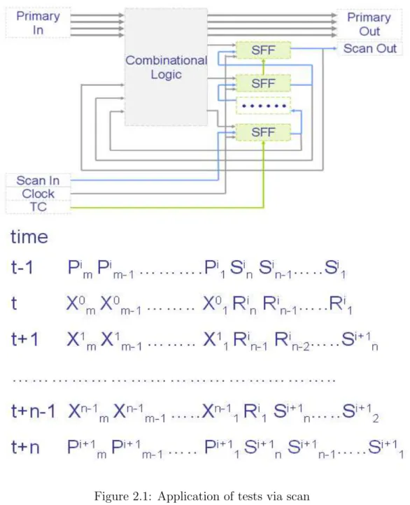
(17) Chapter 2 Low Power Scan Chain Design 2.1. Scan Based Test. In this thesis, we assume that sequential circuit under test(CUT) has full scanned architecture and employs a single scan chain for test application. We use singlestuck-at fault model and ATPG to generate combinational and scan test vectors. Figure 2.1 describes the test application with scan for a CUT which has m primary inputs and n state inputs. The ATPG generates a set of test vectors, each of which is a binary m+n tuples and will be applied to the m primary inputs(p1 ,p2 ,p3 ,...,pm ) and the n state registers(s1 ,s2 ,...,sn ) during test operation. Assume that a test vector, i i i ,..., S1i , is applied to the primary inputs and ,..., P1i , Sni , Sn−1 , Pm−2 V i = Pmi , Pm−1. scan inputs of CUT at time t − 1, and the scan response of CUT to V i , say Rni , i ,..., R1i , is captured in scan registers at time t. Then, the (i + 1)th scan vector, Rn−1 i+1 ,..., S1i+1 , will be shifted in during next n cycles and the scan responses, Sni+1 , Sn−1 i ,..., R1i , will be shifted out. During this scan shifting cycles(t + 1, t + 2,..., Rni , Rn−1. t + n), the value of primary inputs does not have specific values to be applied. These j j , Xm−1 don’t care values are represented by vector Xm ,..., X1j which is applied to. primary inputs at time t + j, where j = 0, 1, 2,..., n-1. At time t + n, the primary i+1 i+1 , Pm−2 input part of V i+1 (Pmi+1 , Pm−1 ,..., P1i+1 ) is applied and the scan responses. of CUT to V i+1 are captured at time t + n + 1. The test application repeats until 5.
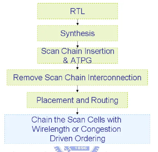
(18) there is no test vector left.. Figure 2.1: Application of tests via scan In IC design flow, scan cells and testing circuit are inserted after synthesis procedure. The scan chain connection will be broken before going into placement phase to prevent scan chain from having great impact on routing congestion. Then, scan cells will be reordered with layout driven chaining algorithm. Figure 2.2 illustrates VLSI design flow and shows where design for testability procedures should be in6.
(19) Figure 2.2: Cell-based VLSI design flow with DFT. Scan chain reordering is performed after placement.. volved in the flow. As for scan chain reordering, there have been many papers about shortening scan chain length and reducing scan chain routing congestion [14] [12]. As chip complexity and operating frequency evolve dramatically, scan chain reordering should not only focus on reducing area overhead but also should take care of power consumption issue. We will review some low power driven scan chain ordering methods proposed in [6] [7] [5] in the following subsections.. 2.2. Power Driven Scan Chain Reordering. The dynamic power, P =Σ 1/2* Cli * f * V dd2 * Si , where Cli is the equivalent output capacitance which is strongly correlated to its fan-out number, V dd is the 7.
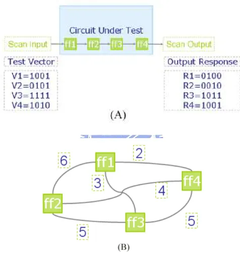
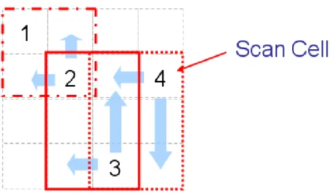
(20) power supply voltage, and Si is switching probability. According to the equation, we can reduce test power by decreasing the number of scan transition activities. In [6], a low power-driven scan chain ordering approach applied a heuristic algorithm to minimize scan chain power. In this algorithm, it used information generated from scan cell insertion tool and automatic test pattern generator, along with scan flip-flops, scan-in test vectors and scan-out response vectors, to produce a LPSC order. The proposed approach procedures are as follows. First, construct a complete undirected graph: vertex represents scan flip-flop and each edge represents possible connection between two scan cells. The weight of each edge represents the total number of bit differences between two scan cells. Figure 2.3(A) illustrates scan flip-flops and scan vectors. They calculate bit differences between each pair of flipflops on the scan-in vectors and output responses. For example, in Figure 2.3(A): d(ff1,ff2)=6,d(ff1,ff3)=3,d(ff1,ff4)=2, d(ff2,ff3)=5,d(ff2,ff4)=4,d(ff3,ff4)=5. Figure 2.3(B) shows the weighted graph example. Second, use greedy heuristic to find low cost Hamiltonian cycle. From the low cost cyclic solution, they estimate power for each flip-flop when it is considering scan-in port. Then, find a minimum cost cutting edge. The solution is the optimal scan cell order with the much lower transition number during scan chain shifting operation.. 2.3. Routing Constrained Low Power Scan Chains. The power driven scan chain reordering approach from previous subsection has drawbacks mainly in creating routing congestion and long scan connection in the design. To show this point, Figure 2.4 shows s9234 benchmark routing result with power driven scan chain reordering. (s9234 is one of ISCAS89 benchmarks and has 211 flip-flops). In Figure 2.4, nodes represent the position of scan cells in the design and edges represent connections between scan cells. Although the power driven approach can efficiently reduce power (27% power reduction compared to length driven scan 8.
(21) Figure 2.3: (A) Example set of scan-in vectors and output response. (B)Complete weighted graph. Nodes represent scan cell and edges represent connection between nodes. The edge weight is bit difference between two scan cells.. 9.
(22) Figure 2.4: Example of power driven chaining scan cells for circuit s9234 obtained from [6]. It contains high routing congestion.. chain reordering), the routing result is not optimal and has high routing congestion. In order to reduce the routing overhead in power driven scan chain ordering, [7] proposes to partition chips with geographic criteria and chain scan flip-flops in each cluster with low power driven order. In this approach, it definitely can shrink LPSC length, but the testing power reduction may be low when there are few flip-flops in a cluster. To improve power reduction ratio in each cluster, [5] proposes a better version on partitioning chips with well distributed scan flip-flops in each cluster. This approach can slightly increase testing power reduction ratio and the total wire length of the scan chain remains almost the same. From the experimental results described in [7] [5](Figure 2.5(A)(B)), we learn. 10.
(23) Figure 2.5: (A)Low power scan chain reordering with geographic constrained approach which is proposed in [7].(B)Instead of partitioning chip with geographic architecture, [5] partitions the chip with well distributed scan cell in each cluster and reorder the scan chain with low power order.. 11.
(24) that the testing power reduction and scan chain connection length are strongly correlated with number of clusters. The more the number of clusters is, the less the power optimization ratio is. That is, if there are more clusters, the power reduction ratio will be less and the scan chain length will be shorter. In fact, we will show that we do not have to partition the chip and obtain the same tradeoff easier.. 12.
(25) Chapter 3 Low Power Scan Chain Optimization During Detailed Placement and Post Placement Phase Although Agrawal et al.,author of [18], has suggested that scan chain reordering should only be executed after place-and-route procedure, this suggestion is based on reducing scan chain routing overhead, decreasing scan chain routing congestion, improving timing violation, etc. From the dynamic power formula, we can find that shortening connection length also has the benefit of lowering loading capacitance and thus reducing switching power. In order to further reduce routing length of LPSC, we implement two methods on shortening LPSC routing length during placement phase and optimizing LPSC after placement phase. From these, we can know how much cost will be charged to improve LPSC routing length. In the following subsections, we show how we implement our detailed placement which can improve LPSC routing cost and how we optimize LPSC routing length in post placement phase. The LPSC order has been decided after test vectors are known, and the connection of LPSC will not be broken when going into the procedures proposed in this section.. 13.
(26) 3.1. Optimizing Low Power Scan Chain during Detailed Placement Procedure. In cell-based VLSI physical design, many efficient placement algorithms have been developed, such as simulated-based placement [21], partition-based placement [8], performance driven placement [15], etc. In order to develop a detailed placer which can keep information for specific cells, such as flip-flops, during placement process, we choose greedy detailed placement as our placement algorithm which is used by Dragon standard-cell placement algorithm [16] [20]. In order to simplify implementation cost, we consider each standard cell occupying a regular bin in a grid graph. Our greedy detailed placement consists of three steps. First, we partition circuit with hMetis [1] which is multilevel hypergraph partitioning scheme. From this partitioning step, we can group cells which have strong connections among them. Second, we construct weighted graph where vertices represent groups and edges represent interconnection between two groups. We use a greedy TSP program to find a low cross interconnection cost order for these groups. We then use this group order to be our row order and generate an initial placement. Third, we randomly choose one base cell, and from the location of base cell, we randomly choose a target cell within window region. Size of window region can be controlled by setting height and width parameters. The search direction can be classified into two types: vertical search and horizontal search, and it is adjustable. From the experiment conducted in [17], the vertical search to horizontal search ratio is recommended to be 1/5. We use direct wire length between base cell and target cell as our cost.We estimate the total wire length cost when swapping process takes place between base and target cells. If the total wire length cost is reduced, we swap base cell and target cell, otherwise the swapping would not occur. Figure 3.1 shows the flow graph of this greedy placement procedure.. 14.
(27) Figure 3.1: Experiment flow of LPSC optimization during placement (A)ISCAS’89 [9] circuit format. We have developed a script to translate it to ISPD98 net format. (B) We use hMetis to partition the benchmark circuit. The number of partition depends on number of square root of gate count. (C) After the circuit is partitioned, we build a weighted graph where vertices represent groups and edges represent interconnection between two groups. (D) From (C), we use heuristic TSP to find a feasible group order. (E) When group order is decided, cells are randomly placed into their corresponding rows. (F)Two cells, base cell and target cell, are randomly chosen. If the swapping procedure can improve the routing cost, the swap will occur.. 15.
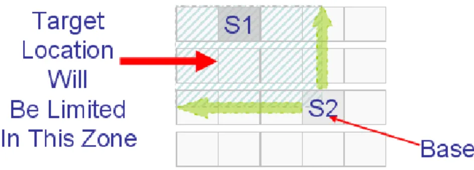
(28) Figure 3.2: The strategy for optimizing LPSC during placement phase. If the chosen base cell is scan cell, the selection of the target cell will be limited into the quadrant where the preceding scan cell is located.. In order to improve LPSC routing cost, we modify the greedy placement strategy as follows. Instead of breaking scan chain connection, we order the scan chain with low power order and try to optimize its routing length in detailed placement phase. In the detailed placement process, if the chosen base cell is scan cell, the selection of the target cell will be limited into quadrant where the preceding scan cell is located. And if the base cell is not scan flip-flop, the placer performs normal greedy swapping strategy. Figure 3.2 shows how we define the target cell search range.. 3.2. Optimizing Low Power Scan Chain during Post Placement Phase. Optimizing LPSC during placement process may cause some gates not finding their feasible positions. From the experimental result, we learn that scan chain will have about 30% shorter routing length by pulling scan cells closer but the design will have poor routing cost and will get worse when design is larger. To our understanding, it is not good to have better LPSC routing performance while sacrificing the total routing cost of the designs.While testing power is the critical issue in modern VLSI design, physical challenge is also essential as process shrinks. Solving low power scan cell wire length problem may not be a good idea. In order to eliminate this 16.
(29) Figure 3.3: We search feasible location for some specific scan cell between itself and its predecessor and compare swapping cost for each location in this specific region. If there is a feasible location to swap, the swapping procedure will be performed.. impact in physical design, we do not optimize LPSC during placement but refine it in post placement phase instead. After placement procedure, we can have physical information for each scan flip-flop. Then, the optimizing process goes with checking feasible position for each scan cell. For example, Scan Cellj will be searched for suitable location between itself and its predecessor Scan Cellj−1 . Scan Cellj will estimate swapping cost for each cell in specific region. If there are several locations which can reduce both chip routing cost and scan chain interconnection length, the most feasible cell, which is closest to predecessor of Scan Cellj and has no impact on previous optimized placement, will be selected to swap with Scan Cellj . The example is as shown in Figure 3.3. The experimental results show that scan chain routing length can be reduced by 1% to 3% with no influence on previous optimized placement result.. 17.
(30) Chapter 4 Scan Chain Reordering with Power and Routing Cost Minimization In previous works ( [7] [5]), they focus on chaining scan cells with power driven order in each cluster and find that test power reduction ratio is strongly correlated with number of clusters. They then chain each cluster with a knowledge based architecture. Although [7] and [5] both can reduce routing overhead which is induced by power driven scan cell chaining by partitioning the design, these approaches may omit some good choices of scan cell pairs which have both low transition number and short connection length. In order to consider test power and routing length minimization, we propose reordering scan chain with cost function which can take both power and routing length into consideration. In this way, we can make scan chain reordering process to find better scan chain order solution without limiting in specific regions. In the following sections, we will delineate how the edge weight is defined and how a good scan chain order can be found.. 18.
(31) 4.1. Weighted Graph Construction Using Power and Routing Cost. In power driven scan chain ordering [6], we can definitely get low transition scan chain order. However, this approach not yet considered scan chain physical information in the design and resulted in routing cost issue. In order to improve routing overhead in LPSC ordering, we construct a weighted undirected graph G(V ,E) and use distance cost and bit difference cost between each pair of flip-flops to obtain edge weight. Vertices represent scan cells and edges represent connections between scan cells. The edge weights are given by Edge weight(i, j) = (1 − β) ∗ Dist(i, j)/L + β ∗ Bit Dif f (i, j)/N where Dist(i, j) is the direct connecting distance between ith scan cell and jth scan cell, Bit dif f (i, j) is number of bit differences between test vectors in i-th scan cell and j-th scan cell, L is diagonal length of the chip, N is total number of scan-in and response vectors, and β is the parameter that controls how much effort we will pay attention to scan power consumption and it is ranged from 0 to 1. Because the units of Dist(i, j) and Bit dif f (i, j) are differently scaled, we normalize direct connecting distance of scan cell i and j by diagonal distance of the chip and normalize number of bit difference by total number of scan-in and response vectors.. 4.2. Efficient Heuristic in Finding Minimum Cost Scan Chain Order. After weighted graph is constructed, we need to find a path with minimum cost. This problem can be formulated as a TSP problem, which is known as NP-complete. In order to generate an acceptable solution efficiently, we implement a heuristic. 19.
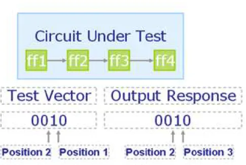
(32) algorithm to get a competent low cost solution.1 Our algorithm is as follows: Heuristic TSP Algorithm begin while un − toured nodes exist minimum cost = ∞; minimum cost edge = 0; for each edge if edge cost<minimum cost if edge does not f orm loop when edge is added into tour minimum cost:=edge cost; minimum cost edge:= edge; end end end Add Edge into Tour(minimum cost edge); Delete Node(node); //delete this nodef rom //un − toured nodes Detelte Edge(minimum cost edge); //delete this edge //f rom edge database end end The complexity of this algorithm is O(|V ||E|), where |V | is number of flip flops and |E| is number of edge in the weighted graph. After we find the low cost scan chain order, we can decide scan-in port and scan-out port of scan chain for power minimization.. 4.3. Power Estimation for Scan-in and Scan-out Ports Determination. When scan chain order has been decided, we need to define scan-in and scan-out ports because the number of transition activities is not only related to the number of bits difference between scan cells but also strongly correlated to their relative positions. In order to choose which one of scan cells in the beginning of the scan 1. Since TSP is a NP-complete problem, there are more enhanced solution by using linear programming and cutting plane [3].. 20.
(33) chain, we need to estimate power for these two orders. To estimate scanning power dissipation, we use weighted transition model proposed in [19]. For example, scanin vector v1v2v3v4 has value 1010 and the scan-in order begins from v4. This vector has transition t1 between v3 and v4, t2 between v2 and v3, and t3 between v1 and v2. As for t1, when v4 is loaded into scan chain, t1 will transit through the entire scan chain and t2 will transit until reaching last 2 scan cells. t3 will stop right after scanning into scan chain. Hence, we can observe that t1, t2, and t3 have different power dissipation effects on circuit due to different positions. In order to estimate scan-in and scan-out power in our scan chain order, we use the formula from [19]: W eight T ransition = Σ(Size of Scan Chain− P osition of T ransition) For instance, our scan-in vector v1v2v3v4 has value 0010 and scan-in vector is loaded with v4 first. Then scan-in W eight T ransition will be (4-1) + (4-2) =5. As for scan-out vector, if we have scan-out vector o1o2o3o4 with 0010 and is scanned out from o4 to o1, then scan-out W eight T ransition will be (4-3) + (4-2)=3. Then the W eight T ransition is 5 + 3=8. The relative position information and transition are illustrated as shown in Figure 4.1. From this power estimation function, we can decide which one of scan cell in the beginning scan chain to be scan-in port and which one to be scan-out port for this low power dissipation scan chain.. 21.
(34) Figure 4.1: Example set of scan-in and scan-out vectors. The beginning position of transiting activity can affect the number of transition.. 22.
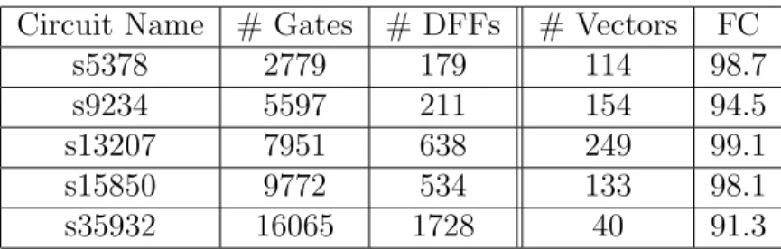
(35) Chapter 5 Experimental Results We experiment with our approach on circuit benchmark of ISCAS’89 family [9]. In order to simplify scan-based test power estimation, we use number of transition in scan chain as dynamic power unit and normalize it with routing driven scan chain ordering to highlight the power reduction ratio. The results are verified using PrimePower [4] and the estimation error is within 3%.. 1. As for interconnection. length of scan cells, we use direct connection length between scan cells. The circuit characteristics and testing vector information are shown in Table 5.1. The deterministic testing vectors are generated from Syntest-TurboScan [2]. The lost of fault coverage(FC) is due to circuit design and aborted faults. The second column of the first part in the table shows the number of gates which NOT gates are included and the third column shows the number of D flip-flops. In the second part of the table, we show the number of testing vectors for each circuit benchmark and corresponding fault coverage. Note that the value in Table 5.1 will not be changed during the process. Our experiment flow is shown in Figure 5.1. At the beginning, we synthesize ISCAS’89 benchmarks and use TurboScan to replace flip-flops with scan flip-flops. 1. We assume that fan-out loading of each scan flip-flop are the same. However, the fan-out loading of each scan flip-flop may differ from each other. This is why we have variation in estimating switching power.. 23.
(36) Table 5.1: Characteristics of ISCAS’89 benchmark and its DFT information Circuit Name s5378 s9234 s13207 s15850 s35932. # Gates 2779 5597 7951 9772 16065. # DFFs 179 211 638 534 1728. # Vectors 114 154 249 133 40. FC 98.7 94.5 99.1 98.1 91.3. We use ATPG to generate a set of scan vectors. From the scan vectors, we can transform the scan chain into LPSC architecture. Instead of breaking scan chain order, we preserve LPSC order when going into placement procedure. Then, we work on optimizing LPSC in detailed placement step, in post placement process, and in routing procedure separately. In the following sections, we will show the experimental results for these three approaches.. 5.1. Detailed Placement with Minimizing Wirelength of Low Power Scan Chain. Table 5.2 shows experimental result of detailed placement with LPSC. In the second column, we show the power reduction ratio (P R) which is normalized to dynamic power with wire length driven scan chain reordering design. We show total wire length reduction ratio (W LR) of this approach in third column and LPSC wire length improvement ratio (LP SC W L Imp.) in fourth column. From the table, we learn that although we can enormously improve routing cost of LPSC in placement phase, it is not good to trade the performance loss in circuit design.. 24.
(37) Figure 5.1: Modern VLSI design flow with DFT. Scan chain reordering is performed after placement.. Table 5.2: Experimental result of detailed placement with minimizing wire length of low power scan chain Circuit Name s5378 s9234 s13207 s15850. P R(%) 34.52 27.08 34.22 30.03. W LR(%) -6.1 -7.3 -12.2 -14.35. 25. LP SC W L Imp. (%) 29.6 35.8 32.9 34.3.
(38) Table 5.3: Experimental result of optimizing low power scan chain during post placement phase Circuit Name s5378 s9234 s13207 s15850. 5.2. P R(%) 34.52 35.8 34.22 30.03. W LR(%) -0.68 0.16 4.48 2.2. LP SC W L Imp. (%) 1.5 2.8 1.09 2.1. Optimizing Low Power Scan Chain during Post Placement Phase. Table 5.3 shows experimental result of optimizing LPSC during post placement phase. The second column of this table is power reduction ratio P R of scan chain. The third column shows total wire length reduction ratio (W LR) comparing with normal condition which has no LPSC optimizing procedure in post placement. The routing improvement ratio of LPSC (LP SC W L Imp.) is shown in fourth column. We learn that we actually do not affect the previous optimized placement result, but we can slightly improve it, instead. In the fourth column of the table, it is shown that there are only 1-2% improvement and this is not effective. It is because most placement cells have reached stable state and have less probability to move to another locations. The LPSC optimizing process in this phase may not have much meliorable space. Figure 5.2 shows the weakness in improvement space of this approach.. 5.3. Scan Chain Reordering with Power and Routing Cost Minimization. The experimental results of third approach are shown in Table 5.4. The second row P R represents power reduction ratio and W L represents routing length of all scan cells. The placement result is generated from the placer which follows the design 26.
(39) Figure 5.2: These figure goes with ISCAS’89 s382 benchmark which has 21 flip-flops. (A) Low power scan chain architecture before optimizing process. (B)Low power scan chain architecture after optimizing process. We can learn that there is tiny improving space for using greedy swapping technique in this phase. 27.
(40) of Dragon standard-cell placement tool [20] [16]. We also follow the assumption from [7] that there is a strong connection between routing length and routing congestion. We start by setting β with 0 and increase its value by 0.2 until β is equal to 1. For each benchmark, we show its power reduction ratio and scan chain interconnection length. All power reduction ratios are normalized to ratios with β=0 of each benchmark which has best routing cost and poorest power consumption. From Table 5.4, we can see the tradeoff between testing power and scan chain routing cost. For example, although s13207 has 6.9% higher power reduction ratio in β=0.4 than that in β=0.2, it costs 43.9% longer in wire length. With our well defined cost function, we observe that the power saving ratio is almost linearly increasing with β from 0 to 1. From this result, testing designers can control tradeoff between power consumption and routing overhead more intuitively. Table 5.4: Average power reduction and routing length with β=0 to 1. This shows the tradeoff between power consumption and routing cost of scan chain ordering.. β value β=0.0 β=0.2 β=0.4 β=0.6 β=0.8 β=1.0. s5378 WL P R(%) 6.37E+2 0 6.79E+2 8.99 8.43E+2 16.23 1.21E+3 23.56 1.91E+3 27.96 4.44E+3 34.52. P (%) 0 11.80 15.30 19.30 22.70 27.08. s9234 WL 9.03E+2 1.09E+3 1.48E+3 2.41E+3 3.88E+3 7.08E+3. s13207 WL P (%) 1.95E+3 0 2.37E+3 8.74 3.41E+3 15.13 5.72E+3 21.34 1.16E+4 28.9 2.98E+4 34.22. s15850 WL P (%) 2.05E+3 0 2.31E+3 8.29 2.84E+3 13.56 3.93E+3 18.17 6.68E+3 23.89 2.33E+4 30.03. s35932 WL P (%) 1.78E+4 0 1.78E+4 0.66 1.79E+4 3.26 1.83E+4 8.07 1.96E+4 15.24 7.52E+5 39.23. We have implemented [7] to compare the experimental results with our approach. Table 5.5 shows the experimental result of [7] in our execution platform. As previously shown, all power reduction ratios of each benchmark are normalized to results of routing length driven scan chain reordering. The results show that the more clusters we use, the less the power reduction is and the shorter the scan chain length is, and the trend is the same as shown in [7]. Furthermore, the advantage of our approach is clearly shown in Figure 5.3, which we compare the result from Table 5.5 and our proposed approach. The horizontal axis is routing wire length 28.
(41) and the vertical axis represents power reduction ratio compared with pure routing driven scan chain reordering when β=0. We can see that our approach has more power reduction ratio under the same routing overhead. We also have less routing overhead under the same power reduction ratio. In Figure 5.4, we show scan chain routing graph of s9234 benchmark with four clusters in (A) and β=0.6 in (B). From Figure 5.4, we can explicitly observe the advantage over routing congestion under the same test power saving ratio which is around 19% in this example. As for approach in [5], which partitions chip with well distributed flip-flops, their approach has 1-3% improvement in power reduction ratio and has about the same routing overhead compared with [7] in benchmark s9234. We then deduct from Table 5.5 that our approach has both better power reduction and routing cost compared with approach in [5]. Table 5.5: Experimental results of approach in [7] in our platform # cluster 1 2 4 9 16 36 64 100 256 3136 1. s9234 WL P ower(%) 7.08E+3 27.08 5.09E+3 21.04 3.78E+3 19.02 2.84E+3 18.28 2.54E+3 17.26 1.87E+3 14.81 1.73E+3 10.52 1.55E+3 7.95 1.25E+3 4.18 9.54E+2 0.57 Routing Driven Scan Chain Reordering 6.94E+2 0. 29.
(42) Figure 5.3: Comparison of experimental results with approach in [7] and ours, showing that our approach has lower routing cost under the same power reduction ratio.. 30.
(43) Figure 5.4: Experimental result of benchmark s9234. (A) By approach in [7]. The design is partitioned into four clusters and has power saving ratio 19.02%. (B) By our approach. The β is set to 0.6 and has power saving ratio 19.30%. It is clear that our approach provide better wiring with the same power saving ratio. 31.
(44) Chapter 6 Conclusion and Future Work In this thesis, we have shown several approaches on optimizing LPSC in physical design and their tradeoffs in previous sections. With the LPSC reordering, we can alleviate both test power and routing overhead issues on scan chain design. Since we do not constrain chaining scan cells in a specific cluster region, our approach has more freedom to choose better scan cell connection. With well defined cost function for weighted graph, we can also obtain better test power and routing cost optimization more explicitly. In the past, scan chain reordering focused on shortening connection length, reducing routing congestion, making TSP algorithm more efficient, moderating scan chain timing violation, etc. These scan chain optimization approaches may alleviate impact on routing overhead or timing convergence in the design. As scan based BIST test architecture becomes more popular in modern ASICs and SoCs, scan test power problem should also be paid much attention to. From our experimental results, we can control parameter to adjust about 30% scan test power reduction ratio. While the optimizing degree in scan test power is strongly correlated with scan chain routing overhead, we can not always to have β=1.0 which has best scan test power reduction ratio but poorest routing congestion. On the other hand, scan test power reduction ratio generating by considering both power and routing over-. 32.
(45) head may not be enough for test mode in modern circuit design since test mode may consume twice more power than normal function mode. In order to further reduce test power, we can cooperate our scan chain reordering approach with multiple scan chains architectures [13]. Since multiple scan chains architectures can shorten transition shifting path, this can enormously reduce switching per scan cell. We have experimented on two scan chains architecture on benchmark s9234 and found that we can have 50% transition reduction ratio with normal wire length driven scan chain reordering and 62% transition reduction ratio in our reordering approach with β=1.0. Again, we can control scan test power reduction ratio from 50% to 62% by adjusting β. To further reduce test mode power, we can add low power ATPG test patterns in the design and use this technique to collaborate with our reordering approach and multiple scan chain architecture. We will focus on integrating these technique and continue discussing low power test architecture in our future work.. 33.
(46) Bibliography [1] “http://www-users.cs.umn.edu/ karypis/metis/hmetis/”. [2] “http://www.syntest.com/”. [3] “http://www.tsp.gatech.edu/”. [4] PrimePower. Synopsys Inc. [5] Y. Bonhomme, P. Girard, L. Guiller, C. Landrault, S. Pravossoudovitch, and A. Virazel. “Design of Routing-Constrained Low Power Chains”. In IEEE Proceedings, Design, Automation and Test in Europe Conference and Exhibition, pages 62–67, 2004. [6] Y. Bonhomme, P. Girard, C. Landrault, and S. Pravossoudovitch. “Power Driven Chaining of Flip-Flop in Scan Architectures”. In IEEE International Test Conference, pages 796–803, 2002. [7] Y. Bonhomme, T. Yoneda, H. Fujiwara, and P. Girard.. “Efficient Scan. Chain Design for Power Minimization during Scan Testing Under Routing Constraint”. In VLSI Test Symposium, pages 488–493, 2003. [8] M. A. Breuer. “A Class of Min-Cut Placement Algorithms”. In Proceedings IEEE/ACM Design Automation Conference, pages 284–290, 1997.. 34.
(47) [9] D. Bryant F. Brglez and K. Kozminski. “Combinational Profiles of Sequential Benchmark Circuits”. In Proceedings Internationl Symposium on Circuits and Systems, pages 1929–1934, 1989. [10] P. Girard. “Survey of Low-Power Testing of VLSI Circuit”. In VLSI Test Symposium, pages 82–92, 2002. [11] A. Grouch. “Design-for-Test for Digital IC’s and Embedded Core Systems”. Prentice Hall, 1999. [12] M. Hirech, J. Beausang, and Xinli Gu. “A New Approach to Scan Chain Reordering Using Physical Design Information”. In VLSI Test Symposium, pages 348–355, 1998. [13] Mani Soma Kambiz Rahimi.. “Layout Driven Synthesis of Multiple Scan. Chains”. In tcad, pages 317–326, 2003. [14] K.-H. Lin, C.-S. Chen, and T.T Hwang. “Layout-driven Chaining of Scan flipflops”. In IEEE Proceedings Computers and Digital Techniques, pages 421–425, 1996. [15] E. S. Kuh M. A. B. Jackson. “Performance-Driven Placement of Cell Based IC’s”. In Proceedings IEEE/ACM Design Automation Conference, pages 370– 375, 1989. [16] X. Yang M. Wang and M. Sarrafzadeh. “Dragon2000: Standard-cell Placement Tool for Large Industry Circuits”. In Proceedings IEEE/ACM International Conference on Computer-Aided Design, pages 260–263, 2000. [17] Xiaojian Yang Majid Sarrafzadeh, Maogang Wang. “Modern Placement Techniques”. Springer, 2002.. 35.
(48) [18] Vishwani D. Agrawal Michael L. Bushnell. “Essentials of Electronic Teesting for Digital, Memory, and Mixed-Signal VLSI Circuits”. Kluwer Academic Publishers, 2000. [19] R. Sankaralingam, R.R. Oruganti, and N.A Touba. “Static Compaction Techniques to Control Scan Vector Power Dissipation”. In VLSI Test Symposium, pages 35–40, 2000. [20] M. Sarrafzadeh and M. Wang. “NRG: Global and Detailed Placement”. In Proceedings IEEE/ACM International Conference on Computer-Aided Design, pages 164–169, 1997. [21] Sangiovanni-Vincentelli A. Sechen, C. “The TimberWolf placement and routing package”. In solid, pages 510–522, 1985. [22] Seongmoon Wang and S.K. Gupta. “ATPG for Heat Dissipation Minimization during Scan Testing”. In Proceedings IEEE/ACM Design Automation Conference, pages 614–619, 1997. [23] Y. Zorian. “A Distributed BIST Control Scheme for Complex VLSI Devices”. In VLSI Test Symposium, pages 4–9, 1993.. 36.
(49) 自傳. 許力中,1980 年 10 月 17 日生,台灣省台中市人◦ 2003 年自交通大學電子工 程系畢業,繼續進入交大電子工程研究所攻讀碩士學位,研究興趣為超大 型積體電路實體自動化設計與計算機結構,主修為數位電路設計與電腦輔 助設計◦論文題目為「低功率循序串列於細部佈局、佈局之後及繞線上最佳 化方法研究」◦.
(50)
數據
![Figure 2.4: Example of power driven chaining scan cells for circuit s9234 obtained from [6]](https://thumb-ap.123doks.com/thumbv2/9libinfo/8139875.166628/22.892.154.744.158.698/figure-example-power-driven-chaining-cells-circuit-obtained.webp)
+7
![Figure 2.5: (A)Low power scan chain reordering with geographic constrained ap- ap-proach which is proposed in [7].(B)Instead of partitioning chip with geographic architecture, [5] partitions the chip with well distributed scan cell in each cluster and reor](https://thumb-ap.123doks.com/thumbv2/9libinfo/8139875.166628/23.892.241.657.203.979/reordering-geographic-constrained-partitioning-geographic-architecture-partitions-distributed.webp)
![Figure 3.1: Experiment flow of LPSC optimization during placement (A)ISCAS’89 [9] circuit format](https://thumb-ap.123doks.com/thumbv2/9libinfo/8139875.166628/27.892.138.804.333.733/figure-experiment-lpsc-optimization-placement-iscas-circuit-format.webp)
相關文件
87 Eivind Almaas and Albert-László Barabási (2006), “Power laws in biological networks”, in Power Laws, Scale-Free Networks and Genome Biology, Ed. Karev (Eurekah.com and
• Each student might start from a somewhat different point of view and experience the encounters with works of art and ideas in a different way... Postmodern
• Learn strategies to answer different types of questions.. • Manage the use of time
To help students achieve the curriculum aims and objectives, schools should feel free to vary the organization and teaching sequence of learning elements. In practice, most
Certified Information Systems Security Professional (CISSP). Certified Information Systems Security
Explain how home users, small office/home office users, mobile users, power users, and enterprise users. each interact with
In this chapter, a dynamic voltage communication scheduling technique (DVC) is proposed to provide efficient schedules and better power consumption for GEN_BLOCK
Though there’s a growing trend of employing famous Hollywood actors to voice characters in order to provide movies with star power, there are still many unknowns but
