S-band gain-clamped grating-based
erbium-doped fiber amplifier by forward optical
feedback technique
Chien-Hung Yeh 1,*, Ming-Ching Lin 3, Ting-Tsan Huang 2, Kuei-Chu Hsu 2 Cheng-Hao Ko 2, and Sien Chi 2, 3
1 Information and Communications Research Laboratories,
Industrial Technology Research Institute, Chutung, Hsinchu 310-40, Taiwan
2 Department of Electrical Engineering, Yuan Ze University, Chung-Li 320-03, Taiwan 3 Department of Photonics & Institute of Electro-Optical Engineering,
National Chiao Tung University, Hsinchu 300-10, Taiwan
Abstract: An S-band gain-clamped erbium-doped fiber amplifier module, employing a fiber Bragg grating to serve as a reflected element for lasing a saturated tone injected into the module by forward optical feedback method, is proposed and investigated experimentally. Moreover, the performance and behavior of the gain and noise figure in the proposed gain-clamped S-band fiber amplifier have also been discussed in the effectively wavelength range of 1478 to 1520 nm.
©2006 Optical Society of America
OCIS codes: (140.4480) Optical amplifiers; (060.2320) Fiber optics amplifiers and oscillators
References
1. B. Clesca, “Flat-gain amplifiers and transmission in WDM networks,” Tech. Dig. Optical Amplifiers and their Applications, Monterey, CA, Paper FA1, 54–57 (1996).
2. C. Jiang, W. Hu, Q. Zeng, and S. Xiao, “Novel split-band erbium-doped fiber amplifier,” Opt. Laser Technol. 35, 251-256 (2003).
3. C. H. Yeh, C. C. Lee, and S. Chi, “120-nm bandwidth erbium-doped fiber amplifier module in parallel configuration,” IEEE Photonics Technol. Lett. 16, 1637-1639 (2004).
4. Y. H. Lu and S. Chi, “All-optical gain-clamped wideband serial EDFA with ring-shaped laser,” Opt. Commun. 229, 317-323 (2004).
5. Q. F. Jiang, X. M. Liu, Q. Wang, and X. Feng, “Dynamically gain control in the serial structure C+L wideband EDFA,” IEEE. Photonics Technol. Lett. 16, 87-89 (2004).
6. X. Fang, T. Jin, Y. Wang, X. Liu and J. Peng “A simple algorithm for wide-band channel-power clamped EDFA,” Opt. Commun. 213, 285-292 (2002).
7. Y. H. Lu, L. H. Su, and Y. K. Chen, “Optically gain-clamped wideband erbium-doped fiber amplifier using a common figure-eight feedback-loop lasing light,” Opt. Commun. 229, 293-298 (2002).
8. K. Inoue, "Gain-clamped fiber amplifier with a loop mirror configuration", IEEE Photonics Technol. Lett.,
5, 533-535 (1999).
9. M. Cai, X. Liu, J. Cui, P. Tang, D. Liu, and J. Peng, “Study on noise characteristic of gain-clamped erbium-doped fiber-ring lasing amplifier,” IEEE Photonics Technol. Lett. 9, 1093-1095 (1997).
10. M. A. Arbore, Y. Zhou, G. Keaton, and T. J. Kane, “30 dB gain at 1500 nm in S-band Erbium-doped silica fiber with distributed ASE suppression,” in Proc. SPIE, Optical Devices for Fiber Communication IV,
4989, 47-52 (2003)
11. K. H. Lai and S. Chi, “Gain-clamped erbium-doped waveguide amplifier module with fiber Bragg grating
using optical feedback,” Jpn. J Appl. Phys. 44, 4009-4011 (2005). 1. Introduction
Wide-band erbium-doped fiber amplifiers (EDFAs) are effective to increase the number of wavelength division multiplexing (WDM) channels in 1.5-μm optical transmission and routing network [1]. Nowadays, the EDFA with 120 nm bandwidth has been achieved theoretically and experimentally [2, 3]. On the other hand, in dynamic WDM networks that employ reconfigurable optical add-drop multiplexers or carry burst traffic in optical domain,
power transient induced by the slow response of erbium doped fiber amplifiers (EDFAs) is a challenging issue. The transient effects can be suppressed by using either electric or optical control, or the combination of both methods. Among these schemes, optical gain clamping is a commonly used technique. However, there have been only a few experiments [4-8] performed on C- plus L-band amplifiers with gain clamping. In these works serial configurations [4, 5] were used, inevitably introducing crosstalk between the C- and L-band signals. The parallel configuration [8] can avoid the crosstalk, but the counterpropagating of the signal and the laser light leads to a high NF [9]. Recently, an S-band (1460 to 1520 nm) EDFA, which uses depressed cladding design and 980 nm pump laser to generate EDF gain extension effect, has been studied [10]. Therefore, the gain clamping technique is expected to extend to S-band by using this S band amplifier.
In this study, we present an S-band gain-clamped EDFA by a forward optical feedback method, using different fiber Bragg gratings (FBGs), which serve as the reflector for lasing a saturated tone injected into the proposed amplifier, over the operating region of 1478 to 1520 nm. Compared with ref. 11, the proposed S-band gain clamped EDFA not only uses different saturated tone injected into the amplifier, but also adjusts various optical powers for investigating the behaviors of the EDFA. Moreover, the gain-clamped behavior and performance has also been investigated experimentally under different operation conditions.
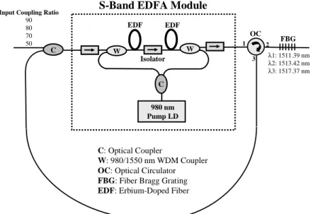
Input Coupling Ratio
90 80 70 50 980 nm Pump LD W EDF EDF W Isolator C
S-Band EDFA Module
OC FBG 1 2 3 λ1: 1511.39 nm λ2: 1513.42 nm λ3: 1517.37 nm C C: Optical Coupler W: 980/1550 nm WDM Coupler OC: Optical Circulator FBG: Fiber Bragg Grating EDF: Erbium-Doped Fiber
Fig. 1. Experimental setup for a gain-clamped S-band EDFA module by forward optical feedback method.
2. Experiment setup
The lasing action at a wavelength can fix the total population inversion in a homogeneously broadened medium. Therefore, the gain for all the wavelengths only dependent on their absorption and emission cross sections and the overlapping factor. Any variation in input signal powers will be compensated by the adjustment of the lasing signal power. As a result, each signal wavelength experiences a constant gain through this optical amplified system, independent of signal power variation caused by operation such as channel adding or dropping. Based on this principle, figure 1 shows the experimental setup for a gain-clamped S-band EDFA module by forward optical feedback method. The proposed structure consists of an S-band EDFA, a 3-ports optical circulator (OC), a 1×2 optical coupler (C) and a FBG. The C has the input coupling ratios of 90, 80, 70 and 50 % for the input signal in Fig. 1, respectively. The optical coupler with different input coupling ratio governs the forward
injected power level of each saturated tone individually. The FBG acts as a mirror for generation a laser in the wavelength band of an erbium S-band amplifier. The laser is injected in forward direction in order to clamp the gain profile of the amplifier. In this experiment, we use three FBGs (with different central wavelengths and reflectivities) and four optical couplers (with different coupling ratio) to govern a various injected wavelength and power levels for observing the performance of the S-band gain-clamped EDFA module.
Wavelength (nm)
1465 1475 1485 1495 1505 1515 1525 1535G
a
in
/ No
ise Fig
u
re (
d
B)
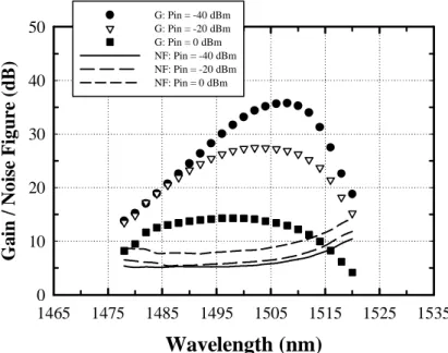
0 10 20 30 40 50 G: Pin = -40 dBmG: Pin = -20 dBm G: Pin = 0 dBm NF: Pin = -40 dBm NF: Pin = -20 dBm NF: Pin = 0 dBmFig. 2. Gain and noise spectra of the original S-band EDFA over the wavelength region of 1478 to 1520 nm, while the input signal power Pin = 0, –20 and –40dBm, respectively.
The S-band EDF inside EDFA module has a depressed cladding design in order to provide a sharp, high-attenuation, long-wavelength cutoff filter into active fibers. The erbium-doped fibers in the first and second stages have different characteristics. The fiber in the first stage has the fiber length of 20 m, and can provide low noise figure and medium gain by forward pumping. The fiber in the second stage has the fiber length of 30 m, and can produce large output power by backward pumping. In addition, the optical isolator between these two stages can reduce backward amplified spontaneous emission (ASE) and improve noise figure performance. The total pump power of this amplifier module can be up to 280 mW while the bias current is operated at 356 mA. To measure the behaviors and performances of the proposed amplifier module, a tunable laser source (TLS) is used to probe the gain and noise figure spectra, which are observed by an optical spectrum analyzer (OSA) with a 0.05 nm resolution.
3. Results and discussion
Figure 2 shows the gain and noise spectra of an S-band EDFA without gain clamping over the wavelength region of 1478 to 1520 nm, while the input signal power (Pin ) is 0, –20 and –40 dBm, respectively. According to figure 2, the gain and noise figure can reach 27.6 and 5.9 dB at 1504 nm with the input power of –20 dBm, and the saturated output power at 1498 nm can be up to 14.5 dBm with a 0 dBm input power. The noise figures are between nearly 5.3 to 7.5 dB when the input signal power is –20 dBm in the wavelength range of 1478 to 1512 nm. When the input signal power are 0, –20 and –40 dBm at 1510 nm, the observed gain and noise figure are 12.4 and 9.6 dB, 26.4 and 6.8 dB, and 35.3 and 6.5 dB, respectively, as shown in Fig 2. Because some passive components, placed at the signal input and output end, have higher losses in C-band and the splice point of EDF and WDM coupler possesses higher loss, the noise figure of this S-band EDFA module will be slightly degraded.
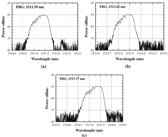
To obtain the S-band gain-clamped EDFA, a FBG is used in the proposed amplifier module for lasing a saturated tone to fix the total population inversion, as seen in Fig 1. In this experiment, we use three FBGs with different central wavelengths and reflectivities successively. Figures 3 show the reflective spectrum of FBG1 to FBG3 individually with the central wavelength of (a) 1511.39 nm, (b) 1513.42 nm and (c) 1517.37 nm. Reflectivities of FBG1 to FBG3 are 91.83%, 93.11%, and 82.98%, respectively. The three S-band FBGs have the maximum wavelength shifts of 2.0 to 2.3 nm while an external strain applied on the FBGs. When the temperature is raised to ~90 ℃, then the central wavelength has nearly 1.2 nm variation. FBG: 1511.39 nm Wavelength (nm) 1510.0 1510.5 1511.0 1511.5 1512.0 1512.5 1513.0 Po wer (d B m ) -85 -75 -65 -55 -45 FBG: 1513.42 nm Wavelength (nm) 1512.0 1512.5 1513.0 1513.5 1514.0 1514.5 1515.0 Powe r (d B m ) -85 -75 -65 -55 -45 (a) (b) FBG: 1517.37 nm Wavelength (nm) 1515.5 1516.0 1516.5 1517.0 1517.5 1518.0 1518.5 Po we r (d B m ) -85 -75 -65 -55 -45 (c)
Fig. 3. The reflective spectrum of FBG1 to FBG4 with the central wavelength of (a) 1511.39 nm, (b) 1513.42 nm and (c) 1517.37 n
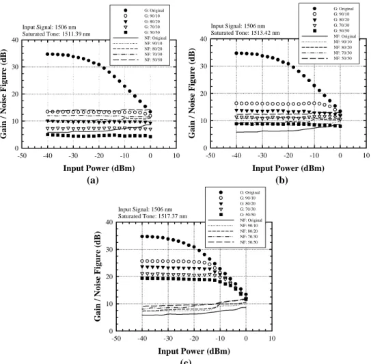
Figures 4 show the gain and noise figure characteristics versus the different power level of input signal at 1506 nm without gain clamping and with the input coupling ratio of C at 90%, 80%, 70%, 50% for the input signal, while the saturated tone at (a) 1511.39 nm, (b) 1513.42 nm, and (c) 1517.37 nm, respectively. Figure 4(a) shows the gain and noise figure spectra versus different input signal power. Figure 4(a) also presents the worse gain and noise profiles at any coupling ratios. Due to the larger gain region around 1508 to 1512 nm (in Fig. 2), the saturated tone will retrieve largest gain to clamp the gain profile in the region and lead to the degradation of noise figure simultaneously. In other words, when a saturated tone at 1511.39 nm injected into the EDFA module will obtain the most Er3+ ion population inversion (obtain largest gain) to clamp the gain profile, it also would produce the lower gain and worse noise figure spectra for other input signals. Then, Figure 4(b) shows that the gain will be kept constant at the input signal power of –10 dBm at an input coupling ratio of 90%, and the constant gains are maintained at nearly 16.1 dB and the noise figure will be distributed at 8.3 to 8.8 dB while the input signal power is lower than –10 dBm. Fig. 4(b) displays the noise
figure of > 10 dB for the input coupling ratio of > 80%. At other operating conductions, the gain and noise figure profiles of Fig. 4(b) also are worse; however, the results are better than that of Fig. 4(a).
Input Signal: 1506 nm Saturated Tone: 1511.39 nm Input Power (dBm) -50 -40 -30 -20 -10 0 10 G a in / N o ise F ig u re ( d B) 0 10 20 30 40 G: Original G: 90/10 G: 80/20 G: 70/30 G: 50/50 NF: Original NF: 90/10 NF: 80/20 NF: 70/30 NF: 50/50 Input Signal: 1506 nm Saturated Tone: 1513.42 nm Input Power (dBm) -50 -40 -30 -20 -10 0 10 G a in / No ise F ig u re ( d B ) 0 10 20 30 40 G: Original G: 90/10 G: 80/20 G: 70/30 G: 50/50 NF: Original NF: 90/10 NF: 80/20 NF: 70/30 NF: 50/50 (a) (b) Input Signal: 1506 nm Saturated Tone: 1517.37 nm Input Power (dBm) -50 -40 -30 -20 -10 0 10 G a in / No ise F ig u re (d B ) 0 10 20 30 40 G: Original G: 90/10 G: 80/20 G: 70/30 G: 50/50 NF: Original NF: 90/10 NF: 80/20 NF: 70/30 NF: 50/50 (c)
Fig. 4. Gain and noise figure spectra without and with the input coupling ratio of 90, 80, 70, 50% for the proposed gain-clamped EDFA when t
When a saturated tone is 1517.37 nm and a input coupling ratio is 50%, the gain will be maintained constant at the input power of < –12 dBm at expense of around 6 dB gain and the gain will be kept at near 19 dB, and noise figure distributes at 8.2 to 9.6 dB, as shown in Fig. 4(c). However, the noise figure has nearly 4.1 dB degradation. When the input coupling ratio is placed at 50 to 80%, the gain will also be kept at the input signal power of < –12 dBm in Fig. 4(c). Figure 4(c) also shows a 28 dB gain dynamic range from –12 to –40 dBm for an 80% input coupling ratio. From these results, when another channel is added or dropped into the amplifier, it almost can’t influence the gain profile for the channel power of < –12 dBm. In another word, if the gain clamped performance will be maintained, the input signal power should be placed in the input dynamic range when another signal is added or dropped. If not, the amplifier can’t carry the gain clamping function. Figure 4(c) also shows that the gain can be kept at 25.3 dB at the input power of < –15 dBm and an input coupling ratio of 90%. As a result, the minimum noise figures of ~1 dB impairment are observed in Fig. 4(c). Compared with Figs. 4(a) to 4(c), Fig. 4(c) has better gain clamping performance and behavior than that of figure 4(a) and 4(b). The experimental results also show that the saturated wavelength of >
1515.69 nm will retrieve the larger clamped gain value and better noise figure. When the saturated tone is removed from the larger gain range of the S-band EDFA, it would obtain better gain and noise figure spectra, as shown in Fig. 4 (c). That is to say, the saturated tone at 1517.37 nm is better choice for the proposed S-band gain clamped EDFA.
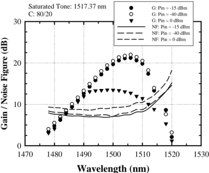
Saturated Tone: 1517.37 nm C: 80/20
Wavelength (nm)
1470 1480 1490 1500 1510 1520 1530G
a
in
/ No
ise
F
ig
u
re
(
d
B)
0 10 20 30 G: Pin = -15 dBm G: Pin = -40 dBm G: Pin = 0 dBm NF: Pin = -15 dBm NF: Pin = -40 dBm NF: Pin = 0 dBmFig. 5. Gain and noise profiles of the S band gain-clamped EDFA in the wavelength of 1478 to 1520 nm with 80% input ratio at the input signal power Pin = 0, –15, and –40 dBm at the lasing wavelength of 1517.37 nm, respectively.
To realize the real gain clamping behaviors, we measure the gain and noise figure spectra in the operating range (1478 to 1520 nm) under an effective input dynamic range in accordance with Fig. 4 (c). Therefore, figure 5 shows the gain and noise profiles of the S band gain-clamped EDFA in the wavelength of 1478 to 1520 nm with an 80% input ratio for the input signal power Pin = 0, –15, and –40 dBm when the lasing wavelength is 1517.37 nm, respectively. Furthermore, the maximum gain at 1502 nm is 24.7 dB at a –40 dBm input power and the maximum gain variations are less then 0.6 dB over the operating wavelength range. In addition, an input gain dynamic range of 25 dB (–40 to –15 dBm) is also obtained in Fig. 5.
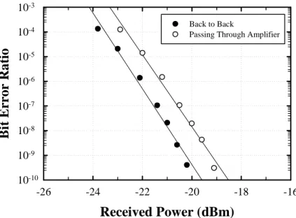
To demonstrate the performance of the proposed gain-clamped EDFA module, a bit error rate (BER) is measured in this experiment. An optical coupler with an 80% input coupling ratio and a FBG with 1517.37 nm central wavelength are used in the gain-clamped EDFA module. A test input signal at 1506 nm is modulated by a 2.5 Gbit/s non-return-to-zero (NRZ) pseudorandom binary sequence with a pattern length of 231–1 on a LiNbO3 electrooptical (EO) modulator. However, the BER performance should be back-to-back without the proposed EDF-based amplifier module, characterizing the transmitter and receiver. A 2.5 Gbit/s optical receiver is used to measure the S-band gain-clamped EDFA system performance. Figure 6 shows the measured BER of the proposed optical amplifier against the received power for the back-to-back-type and the test signal through the gain-clamped EDFA module, when another input channel is added or dropped into the gain clamped EDFA simultaneously. Therefore, while a test input signal passes through the amplifier module, the observed optical power penalty is nearly 1 dB while the BER is 10-9.
Received Power (dBm)
-26 -24 -22 -20 -18 -16Bi
t E
rror
Ra
tio
10-10 10-9 10-8 10-7 10-6 10-5 10-4 10-3 Back to BackPassing Through Amplifier
Fig. 6. Performance of BER at a test signal of 1506 nm in 2.5 Gbit/s modulated system when a 980 nm pump power is 280 mW.
4. Conclusion
In summary, an S band gain-clamped EDFA module, using a FBG serves as a reflected element to lase a saturated tone for clamping gain by forward optical feedback method in the wavelength range of 1478 to 1520 nm, has been proposed and experimentally investigated. Different coupling ratios of an optical coupler and central wavelengths of FBGs are used to show the performance of the gain-clamped EDFA. As a result, the experimental results show that the saturated wavelength of 1517.37 nm will retrieve the better clamped gain value and noise figure for the proposed EDFA module. Moreover, the minimum noise figure of nearly 1 dB impairment is also observed in the proposed amplifier module.
Acknowledgments
This work was supported in part by the National Science Council (NSC) of Taiwan (ROC) under grants NSC 94-2215-E-155-001 and NSC 94-2215-E-155-003.