國立交通大學
材料科學與工程學研究所
碩 士 論 文
多孔性及兩相式(MSQ/高溫起孔洞劑)低介電材料之吸
水性與擴散行為研究
Moisture uptake and diffusion behavior of
MSQ/high-temperature porogen hybrids and porous
low-k materials
研 究 生:鄧鈞元
指導教授:呂志鵬 博士
多孔性及兩相式(MSQ/高溫起孔洞劑)低介電材料之吸水性與擴散行為研究
Moisture uptake and diffusion behavior of MSQ/high-temperature porogen hybrids and porous low-k materials
研 究 生:鄧鈞元 Student:Jun Yuan Teng
指導教授:呂志鵬 Advisor:Dr. Jihperng (Jim) Leu
國 立 交 通 大 學 材 料 科 學 與 工 程 學 系
碩 士 論 文
A Thesis
Submitted to Department of Materials Science and Engineering College of Engineering
National Chiao Tung University in partial Fulfillment of the Requirements
for the Degree of Master in
Materials Science and Engineering
December 2007
Hsinchu, Taiwan, Republic of China
多孔性及兩相式(MSQ/高溫起孔洞劑)低介電材料之吸水性與擴散行為研究
研究生: 鄧鈞元 指導教授: 呂志鵬
國立交通大學材料科學與工程學系碩士班
摘要
本研究利用 Solid-FirstTM製程以Methylsilsesquioxane (MSQ)為介電材料的 基材、poly (styrene-block-4-vinylpyridine) (PS-P4VP)以及 poly (styrene-block- butadiene-block- styrene) (PS-PB-PS)為高溫起孔洞劑。利用自行組裝之石英微量 天坪探討下列三種低介電薄膜之吸水性及水氣擴散行為(1)不同製程溫度的 MSQ 膜(2) 製程溫度為 250 oC 之 MSQ/Porogen 混參膜(3)多孔性薄膜。 研究結果顯示孔隙率較大之多孔性薄膜有較高的吸水量乃是因為表面積與 氫氧基較多之故。以HMDS 改質孔隙率 19.3 %的多孔性薄膜則可降低約 17 %的 吸水量。MSQ/PS-P4VP 混合膜的吸水性較多孔性薄膜高乃因 PS-P4VP 有較高吸 水量之故且高溫起孔洞劑之砒啶與氫氧基之作用使得MSQ/PS-P4VP 有較多之殘 餘氫氧基。MSQ/PS-PB-PS 之吸水性比 MSQ/PS-4VP 差因為 PS-PB-PS 之吸水性 較差之原故。 綜合QCM、C-V、吸附脫附行為顯示水吸附於 MSQ 或 MSQ/Porogen 的方 式以物理吸附為主。在本研究顯示水氣下列兩種方式吸附(1)以凡得瓦耳力附著 於MSQ 或起孔洞劑中、MSQ 與基材之介面以及起孔洞劑與基材之介面而此吸附 方式佔總吸水量的 80 % (2)以氫鍵(Si-O……H2O)附著此吸附方式佔總吸水量
水氣在薄膜中擴散行為大至符合Fickian 擴散方式,但是各種薄膜有幾乎相 同的擴散係數除了高含量高溫起孔洞的薄膜乃是因為孔洞型態改變之故。擴散係 數在高溫起孔洞劑含量20 wt%下保持不變是因為有一層緻密薄膜在表面形成且 為速率控制。而此緻密薄膜可為擴散阻障層,保護CVD、ALD 之先驅物擴散進 入 介 電 材 料 中 。 但 是 PS-PB-PS 系 統 則 無 此 緻 密 薄 膜 , 本 論 文 將 提 出 MSQ/PS-P4VP 表面緻密薄膜形成方式。
Moisture uptake and diffusion behavior of MSQ/high-temperature porogen hybrids and porous low-k materials
Student: Chun-Yuan Teng Advisor: Jihperng (Jim) Leu
Department of Materials Science and Engineering National Chiao Tung University
Abstract
Incorporation of porosity into dielectric materials is a viable method to reduce k-value down to < 2.5. A Solid-FirstTM scheme based on high-temperature porogen, poly (styrene-block-4-vinylpyridine) (PS-P4VP), poly(styrene-block- butadiene-block -styrene) (PS-PB-PS) and methyl-silsesquioxane (MSQ) as the matrix have been employed to prepare porous low-k dielectric in order to circumvent the reliability issues encountered in the integration of as-deposited porous dielectric. The impact of high-temperature porogens, their loadings, and porosities on the moisture uptake and diffusion behavior was investigated using a home-built quartz crystal microbalance (QCM). Three low-k dielectric systems were employed in this thesis to simulate interlayer dielectrics (ILD) at different stages of Solid-FirstTM integration scheme; namely: (1) MSQ films cured at different temperatures up to 400 oC, (2) MSQ/porogen hybrid films cured at 250 oC with various porogen loadings, and (3) their corresponding porous films burned out at 400 oC.
The moisture uptake of porous films cured at 400 oC increased with porosity due to an increase of pore surface area and residual silanol, Si-OH groups. Further
surface Si-OH groups and led to a 17% reduction of moisture uptake for porosity at 19.3%. In addition, moisture absorption of MSQ/PS-P4VP hybrid films cured at 250
oC were greater than porous MSQ ones because of the high water uptake in PS-P4VP
(6.7 wt%) and the increased Si-OH concentration arisen from the interaction between the polar pyridine moiety of porogen with Si-OH in the MSQ matrix In contrast, moisture uptake of MSQ/PS-PB-PS hybrid films was much less than MSQ/PS-P4VP films because of the hydrophobic characteristic of PS-PB-PS.
Based on moisture uptake, sorption/desorption behavior, and HMDS pretreatment by using QCM and CV measurements, we concluded that the moisture uptake in porous MSQ films or MSQ/high-temperature porogens hybrid films in this thesis is solely physical sorption. The physical sorption of moisture uptake underwent by Van der Waals long range force with (1) available surface area within the MSQ or porogen matrix, inside the pores, and at the MSQ/substrate and porogen/substrate interfaces, which contributed < 80% of moisture uptake, and (2) available hydrogen-bonded Si-OH--H2O sites, which were formed immediately after
sample preparation, accounted for < 20% of moisture uptake.
Finally, the moisture diffusion in MSQ/PS-P4VP films and their corresponding porous MSQ films followed Fickian diffusion behavior with almost the same diffusion constant except in the high porogen loading region where pore morphology has changed. The constant diffusion constant at porogen loading below 20% could be attributed to the formation of a rate controlling, dense layer on the top of porous or hybrid low-k films. Such thin but dense layer could serve as a diffusion barrier layer beneficial in certain processing modules. In contrast, no skin layer was observed for MSQ/PS-PB-PS system. The formation mechanism of such a dense layer in MSQ/PS-P4VP system was proposed in the thesis.
誌謝
首先誠摯的感謝指導教授呂志鵬博士,老師悉心的教導使我得以一窺low-k領 域的深奧,不時的討論並指點我正確的方向,使我在這些年中獲益匪淺。老師對 學問的嚴謹更是我輩學習的典範。 兩年裡的日子,實驗室裡共同的生活點滴,學術上的討論、言不及義的閒扯、 讓人又愛又怕的宵夜、趕作業的革命情感、因為睡太晚而遮遮掩掩閃進實驗 室...,感謝眾位學長姐、同學、學弟妹的共同砥礪,你們的陪伴讓兩年的 研究生活變得絢麗多彩。 感謝國原、kima、大龜、阿義學長、幸玲學姐們不厭其煩的指出我研究中 的缺失,且總能在我迷惘時為我解惑,也感謝阿之、冠頭魚、欣源同學的幫忙, 恭喜我們順利走過這兩年。實驗室的阿農、伯政、晉成、王聰明學弟、nikky、 宜甄、先帝學妹們當然也不能忘記,妳的幫忙及搞笑我銘感在心。 女朋友小頭貞在背後的默默支持更是我前進的動力,沒有小頭貞的體諒、包 容,相信這兩年的生活將是很不一樣的光景。 最後感謝國科會(計畫編號NSC95-2221-E009-309、NSC96-2221-E-009-216) 及SRC(計畫編號SRC 2007-KJ-1301)於經費的贊助。Contents
摘要...i
Abstract... iii
Acknowledgements...v
Table Caption ... viii
Figure Caption ... viii
Chapter 1 Introduction ...1
Chapter 2 Literature review ...3
2.1 low dielectric constant materials...4
2.1.1 Dielectric constant ...6
2.1.2 Polarization of material...7
2.2 Integration requirements of low-k materials...10
2.3 Deposition of low-k films ...11
2.3.1 Chemical vapor deposition (CVD) ...11
2.3.2 Spin coating ...11
2.4 Introduction of low-k materials ...13
2.4.1 Silicon-base low-k polymer ...13
2.4.1.a Fluorinated silicate Glass (FSG) ...13
2.4.1.b Carbon doped oxide (CDO) ...14
2.4.1.c Hydrogen silsesquioxane (HSQ)...16
2.4.1.d Methyl silsesquioxane (MSQ) ...18
2.4.2 Organic low-k polymer ...20
2.4.2.a SILKTM...20
2.5 Porous low-k materials ...21
(1) Sol-Gel method ...22
(2) Nano-clustering method ...23
(3) Template method ...23
2.6 Impact of porous materials on IC integration ...26
2.7 Impact of moisture on low-k materials. ...31
Chapter 3 Experimental ...32
3.1 Preparation of low-k films ...36
3.1.1 Chemicals...36
3.1.2 Preparation of low-k precursor solution ...37
3.1.3 Deposition of low-k films ...38
3.2.1 n&k analyzer...39
3.2.2 Specular reflectance Fourier-transform infrared spectroscopy (FIIR)41 3.2.3 Capacitance measurement...41
3.2.4 Focus ion beam (FIB) ...44
3.2.5 Quartz Crystal Microbalance (QCM) ...45
Chapter 4 Result and Discussion ...53
4.1 Optical properties of low-k films...54
4.2 Moisture uptake of low-k films...56
4.2.1 Moisture uptake of MSQ films with different curing temperature ...56
4.2.2 Moisture uptake of porous films………..……….58
4.2.3 Moisture uptake of HDMS modified porous films and MSQ/PS-P4VP hybrid films………...……60
4.2.4 Moisture uptake of MSQ/PS-PB-PS hybrid films ...62
4.3 Dielectric properties...64 4.4 Diffusion behavior ...68 Chapter 5 Conclusions ...77 Reference ...81 Appendix A...87 Appendix B ...92
List of Tables
Table 2.1 Dielectric constants of typical materials at 20 oC ...7
Table 2.2 Requirements of ILD properties ...10
Table 2.3 Film properties of carbon-doped oxide and PECVD SiO2 ...16
Table 2.4 Key material properties of HSQ and MSQ ...20
Table 2.5 Summary of SiLKTM properties ...21
Table 2.6 Various surfactant(S)/inorganic(I) interaction and examples including PH condition ...25
Table 4.1 Moisture uptake of porous MSQ and HMDS modified porous MSQ films...59
Table 4.2 Moisture uptake of MSQ/PS-PB-PS hybrid films ...63
List of Figures
Figure 1.1 (a) dense low-k MSQ matrix cured at 400 °C, (b) solid-firstTM MSQ matrix/porogen hybrids cured at 250 °C, and (c) corresponding porous low-k MSQ films after removal of porogen at 400 °C ...2Figure 2.1 Structures of multilayer interconnect (a) Al metallization and (b) copper metallization...3
Figures 2.2 Cross-sectional view of a three-layer interconnect with orthogonal layout. ...2
Figure 2.3 Relationship between generation node and RC-delay in gate and interconnect for Al/SiO2 and Cu/lok k ...4
Figure 2.4 (a) Capacitor in vacuum (b) Capacitor with dielectric ...6
Figure 2.5 Electronic polarization...8
Figure 2.6 ionic polarization...8
Figure 2.8 Relationship between dielectric constant and applied electric
filed frequency ...10
Figure 2.10 Chemical structure of fluorinated silicate glass at (a) low fluorine concentration and (b) high fluorine concentration ...14
Figure 2.11 Chemical structure of carbon-doped oxide (CDO)...14
Figure 2.12 Chemical structures of precursors for carbon doped oxide ...15
Figure 2.13 Silsesquioxane preparative pathways . ...17
Figure 2.15 Chemical structures of (a) HSQ and (b)MSQ ...20
Figure 2.17 Schematic illustratration of pore formation in nano-clustering23 silica ...23
Figure 2.18 Pore was formed by thermally or chemically removing templating agent or porogen. ...23
Figure 2.19 Ordered and disordered phases of microstructured materials ..24
Figure 2.20 SEM photographs of (a) delamination during CMP process and (b) delamination and failure after wire bonding ...26
Figure 2.21 Penetration of copper into non-continuous sidewall of a porous dielectric...27
Figure 2.22 (a) TEM image of sidewall profile after pore sealing by a thin low dielectric layer , (b) The schematic diagram of sealing concept...28
Figure 2.23 Concept and process flow of Solid FirstTM scheme Figure ....30
Figure 2.24 Low-k material thin film swells upon absorption of moisture .31 Figure 2.25 ...31
Figure 2.26 Leakage current of low-k thin films under wet and dry conditions...32 Figure 2.27 Schematic diagramd of water adsorption onto SiO2 with and
This chapter described the experimental methods and steps, including low-k precursor solution preparation, spin coating, thermal processed,
quantitative measurement of moisture uptake in low-k films by quartz crystal microbalance, and collection of chemical bond information by FTIR, thickness and refractive index by n&k analyzer, pore
morphology by SEM, and dielectric constant by CV-dot measurement. Flow-chart of experimental procedures was summarized in Figure 3.1 ...35 Figure 3.1 Flow-chart of experimental procedures...35 Figure 3.2 Schematic illustration on the preparation of precursor solution.39 Figure 3.3 Typical curve of n&k measurement...40 Figure 3.4 Schematic diagram of a specular reflectance infrared
speectroscopy...41 Figure 3.5 The process flow for fabricating a MIS sample for CV-dot
measurement ...42 Figure 3.6 Shadow mask with three different diameters for CV-dot
measurement ...43 Figure 3.7 The utilization of linear curve fitting of various dot sizes to
minimize the errors from fringes effect and area measurement...44 Figure 3.8 Schematic diagram of a FIB/SEM system...45 Figure 3.9 Schematic diagram of QCM system for moisture uptake
measurement ...50 Figure 3.10 The frequency change of the crystal resonator at 30 oC versus
time during sorption and desoprtion for MSQ/PS-P4VP (10wt%) hybrid film ...51 Figure 3.11 Moisture uptake of MSQ/ PS-P4VP (10wt%) hybrid film as a
function of time...52 Figure 4.1 (a) Refractive index as a function of porogen loading and (b)
Optical dielectric constant as a function of porogen loading...54 Figure 4.2 The correlation between porosity and porogen loading. ...55 Figure 4.3 Moisture uptake behavior of MSQ films cured at 250oC and
400oC...56 Figure 4.4 FTIR spectra of MSQ films cured at at 250 oC and 400 oC ...57 Figure 4.5 Moisture uptake of porous MSQ and HMDS modified porous
MSQ films...58 Figure 4.7 The moisture uptake of MSQ/PS-b-P4VP hybrid films a function
of porogen loadings...62 Figure 4.8 Moisture uptake of MSQ/PS-b-P4VP and MSQ/PS-PB-PS hybrid films ...63 Figure 4.9 Dielectric constants of porous MSQ and HMDS-modified porous MSQ films at dry and RH 100 % conditions. ...65 Figure 4.10 Dielectric constants of MSQ/PS-P4VP hybrid films at dry and
RH 100% conditions...66 Figure 4.11 Series model, parallel model and EMA model of capacitance .67 Figure 4.12 Calculated dielectric constants based on three models: series
model, parallel models, and EMA model as function of loading vs. experimental data ...68 Figure 4.13 Typical fitting curve based on Fickian diffusion ...70 Figure 4.14 Diffusion coefficients of various low-k films versus different
porogen loadings...71 Figure 4.15 FIB/SEM topview of (a) as-cured, (b) after 5-second sputter
porosity based on PS-P4VP porogen. ...72 Figure 4.16 Schematic diagram of a skin layer/porous low-k matrix stack under the diffusion of moisture...73 Figure 4.17 The proposed mechanism for skin layer formation in
MSQ/PS-P4VP hybrid films ...74 Figure 4.18 FIB/SEM top-view of as-cured MSQ/PS-PB-PS hybrid film
with 5% porogen loading...74 Figure 4.19 (a) hydrogen-bonding between silanol and water and (b)
Chapter 1 Introduction
As device scaling continues, RC delay in the backend interconnect becomes the bottleneck [1]. In order to alleviate this problem, copper was first implemented, then low dielectric constant (low k) materials such as carbon-doped oxide or SiLKTM (k~2.6-3.0) was introduced [2, 3]. For dielectric with k<2.2 which is required for 45 nm node and beyond, incorporation of porosity is inevitable to further reduce the k-value. However, porous low k thin film may encounter reliability issues such as (1) delamination and cracks during CMP and other process due to low mechanical strength, and (2) bias-temperature stressing (BTS) failure due to non-continuous side-wall coverage of barrier deposited by atomic layer deposition, chemical vapor deposition or physical vapor deposition process. To circumvent such reliability issues, a novel Solid-FirstTM [4] approach in material design using high-temperature porogen and integration has been proposed to defer the formation of porous dielectric after the completion of a metal layer, then thermally remove the sacrificial, high-temperature porogen. Recently, Che et al. demonstrated porous ultra low-k materials (k~2.0) using an amphiphilic block copolymer (ABC) high temperature porogen, poly (styrene-block-4-vinylpyridine) (PS-P4VP) in the Solid-FirstTM scheme [5]. In addition such approach offers better mechanical strength.
For porous dielectrics, there are additional concerns related to moisture and solvent uptake induced by processing steps such as CMP, post-etch cleaning, post-CMP cleaning or resist removal. The dielectric properties of porous low-k materials will be significantly degraded if residual H2O (Kwater~78) adsorbed in the
matrix and porogen. In addition, the moisture outgassing may destroy diffusion barrier or etch-stop layer during thermal process [6] resulting in delamination or
adsorption behavior, moisture uptake, and outgassing behavior of low-k dielectric materials, especially porous dielectrics involving the matrix/high temperature porogen hybrid in Solid-First scheme at different stages.
Figure 1.1 (a) dense low-k MSQ matrix cured at 400 °C, (b) solid-firstTM MSQ matrix/porogen hybrids cured at 250 °C, and (c) corresponding porous low-k
MSQ films after removal of porogen at 400 °C
In this study, methylsilsesquioxane and high-temperature porogen, PS-P4VP, PS-PB-PS were used as low-k material matrix and template. Specifically, three types of low-k films namely (a) dense low-k MSQ matrix cured at 400 °C, (b) solid-firstTM MSQ matrix/porogen hybrids cured at 250 °C, and (c) corresponding porous low-k MSQ films after removal of porogen at 400 °C, schematically illustrated in Figure 1.1 were employed to investigate the impact of porogens and porosity on the moisture uptake and diffusion behavior using quartz crystal microbalance (QCM). The implication of moisture uptake and diffusion with ILD processing will be also discussed.
This thesis includes chapter 1 Introductions and Motivation, chapter 2 Literature Review, chapter 3 Experimental Method, chapter 4 Results and Discussion, chapter 5 Conclusions.
Chapter 2 Literature review
As the device dimension continuously shrinks towards small size according to
Moore’s law [7], the unit area of silicon wafer contains more and more transistors,
and the chips performance is enhanced. Therefore, the chip price can be lowered by increasing the number of chips on each silicon wafer. On the signal propagation within a chip, the signal delay was controlled not only by gate delay but also by signal propagation within the multilayer interconnect such as Al/SiO2 and Cu/low-k interconnects as shown in Figures 2.1(a) and (b), respectively.
Figure 2.1 Structures of multilayer interconnect (a) Al metallization and (b) copper metallization
Figures 2.2 Cross-sectional view of a three-layer interconnect with orthogonal layout.
In the simple first-order, the RC-delay in the interconnect could be expressed by Equation (2.1) [2].
(2.1)
Where P: line pitch,
W: the metal line width,
S: the spacing between line to line T: the thickness of metal line ρ: metal resistively
ε0: the vacuum permittivity,
k: the relative dielectric constant of dielectrics L: the length of the metal line.
Moreover, the power consumption of device could be obtained by Equation 2.2.
⎟⎟
⎠
⎞
⎜⎜
⎝
⎛
+
⋅
⋅
⋅
⋅
=
2
04
22 22T
L
P
L
RC
delayρ
κ
ε
f
CV
f
P
c d 22
1
⎟
⎠
⎞
⎜
⎝
⎛
=
(2.2)where C: total capacitance V: the supply voltage
f: the operation frequency
fd: the fraction of gate that switches during a clock period.
In general, device scaling increased RC-delay and power consumption due to the increase of line-to-line capacitance. In the previous technology nodes (> 250 nm), interconnect signal delay based on Al aluminum (ρ=2.67μΩ-cm) and silicon oxide (k = 4), could be ignored as compared to gate delay since the dimension of metal wire was large enough as illustrated in Figure 2.3. When the device dimensions scaled below than 250 nm node, the interconnect RC delay of Al/SiO2 became the bottleneck
of signal propagation while power consumption became the critical issue of device performance. In contrast, Cu/low-k interconnect illustrated in Figure 2.3 showed that RC delay was greatly reduced compared to Al/SiO2 at < 250 nm nodes [8]. By
employing (1) copper with low resistivity as interconnect metal line and (2) materials with low relative dielectric constant, the problem of RC-delay of interconnect could be contained. In addition, utilizing low dielectric materials could reduce cross-talk and power consumption. Therefore, low dielectric materials were more important for RF devices.
Figure 2.3 Relationship between generation node and RC-delay in gate and interconnect for Al/SiO2 and Cu/lok k [9]
The industry first introduced copper to replace aluminium into the backend technology in 1997 by International Business Machine Corp (IBM). However, the migration from silicon oxide to low-dielectric constant (low-k) materials was gradual due to its great impact on integration. As a result, the early adoption of low-k preferred the modification of silicon oxide such as fluorinated silicate glass (FSG) (k ~3.5-3.7), then carbon-doped oxide (CDO) (k ~3.2-2.5). Unfortunately, dielectric constants of viable, dense carbon-doped oxides were limited to ≥ 2.5. In order to further lower dielectric constants, the incorporation of pores into low-k materials became necessary since dielectric constant of air was about 1.
However, integrating porous, low dielectric materials into copper dual damascene structure and processes had many problems such as:
(1) The mechanical strength of porous low-k was much worse than silicon dioxide.or FSG
materials would cause reliability issues.
Therefore, the mitigation of mechanical strength and reliability issues in the integration and process development of porous low-k dielectrics is the most critical task in the backend technology of 45 nm node and beyond.
2.1 low dielectric constant materials
2.1.1 Dielectric constant
While electrical filed was applied on a parallel-plate capacitor in vacuum as
shown in Figure 2.4 (a), the capacitance C0 of capacitor was expressed as Equation
2.3.
d
A
V
Q
C
0=
=
ε
0 ... (2.3) Where Q: charge V: voltageA: parallel-plate (electrode area) d: distance between the parallel-plate ε0: vacuum permittivity, 8.85E×10-12 F/m
Figure 2.4 (a) Capacitor in vacuum (b) Capacitor with dielectric
The capacitances depended on geometry of the capacitor. It was directly proportional to the area A of electrode and inversely proportional to their separation d. The A and d were constant for a given capacitors, and ε0 was also a universal constant.
When matter was present between the plates, it would affect the capacitance. For the same capacitor, the ratio of C to C0 wascalled dielectric constant of the
materials, defined as Equation 2.4 below
0
C
C
K
=
………...(2.4)Where C: the capacitance with dielectric present in parallel plate
The dielectric constant K is pure number. Table 2.1 listed the dielectric constants of some commonly used materials [10].
Table 2.1 Dielectric constants of typical materials at 20 oC [10]
Material
K
Material
K
vacuum 1 poly(vinyl chloride) 3.18
air (1 atm) 1.00059 germanium 16
Teflon 2.1 water 80.4
polyethylene 2.25 poly (propylene) 1.5
Benzene 2.28 poly (styrene) 2.4~2.6
2.1.2 Polarization of material [11]
The electric field applied on a material in the parallel plate capacitors would
result in redistribution of electric charge, and then would induce an electric dipole. The phenomenon, redistribution of positive and negative charges within the dielectric material, was called polarization [11]. The materials dielectric properties were mainly
determined by polarizability. The dipole moment in unit volume represented the degree of polarization, which was called polarization strength.
The polarizations included electronic polarization, ionic polarization, orientation polarization and space charge [11]. The redistribution of outer atom electron and inter proton in materials in an electric field was called electronic polarization which was also called atomic polarization as shown in Figure 2.5. The electronic polarization phenomenon disappeared when the absence of the electric filed happened.
Figure 2.5 Electronic polarization
Ionic polarization, as shown in Figure 2.6, was caused by relative displacements between positive and negative ions in ionic crystals such as NaCl.
Figure 2.6 ionic polarization
When an electric filed was applied, the dipole of molecule would align electric filed which was called orientation polarization as shown in Figure 2.7. Space charge was in the dielectric, electrons, protons, and ions which moved around by the applied electric
filed. Charge tended to build up a discontinuous interface in the dielectric, such as the dielectric-electrode interface in film capacitors.
Figure 2.7 orientation polarization [11]
The dielectric constant related to polarization. When an electric filed was applied on parallel plate capacitor, polarizability P; then the capacitance increased as shown in equation 2.5.
V
AP
d
A
C
=
ε
0+
……….(2.5) By combiningk
Pd
V
01
ε
+
=
with equation 2.5, we obtained equation 2.6.
d
A
k
C
=
ε
0
………(2.6)
Besides, the polarization also related to the frequency of electric filed; thus, the dielectric properties of materials were a function of operating frequency as shown in Figure 2.8. The dielectric constants of materials were dependent on operating frequency contributed to electronic, atomic and orientation polarization [12]. At the optical frequency, the primary contribution was electronic polarization because atomic and orientation polarization can not respond so fast.
Figure 2.8 Relationship between dielectric constant and applied electric filed frequency [12]
2.2 Integration requirements of low-k materials
In order to reduce RC-delay, the k value of low-k materials must be lower than traditional SiO2. However, the interlevel dielectric materials (ILD) needed not only
good electrical properties, but also excellent chemical properties, mechanical properties and thermal stability. Desired properties [13] of ILD were shown in following Table 2.2.
Table 2.2 Requirements of ILD properties [13]
Electrical Chemical Mechanical Thermal
Low dielectric constant Isotropic Low dissipation Low leakage current Low charge trapping
High electric filed strength
Good chemical resistance Low moisture uptake <1% Etch rate and selectivity Low gas permeability No metal corrosion Thickness uniformity Good adhesion Residual stress <100Mpa Low shrinkage Crack resistance Tensile modulus High thermal stability CTE <50 ppm/oC Low thermal shrinkage High thermal conductivity
2.3 Deposition of low-k films
There are two major methods, namely chemical vapor deposition and spin coating for depositing low-k thin films in the fabrication of silicon-based IC devices.
2.3.1 Chemical vapor deposition (CVD)
Chemical vapor deposition was a film deposition method, whose utilizing chemical reaction included pyrolysis, reduction, oxidation and/or nitridation on the substrates. The mechanism of CVD deposition consisted of three steps. The first was nucleation, and then the nucleus formed an island which grew into a big island later. Finally, continuous film formed when the island was large enough to contact the others. The films deposited, by low pressure CVD (LPCVD), with more uniform quality since low pressure had lager mean free path [14]. For low-k thin films used in the backend interconnect, plasma-enhanced chemical vapor deposition (PECVD) was commonly employed at 350-450 oC due to the consideration of lowered thermal budget.
2.3.2 Spin coating
The most simple and common technique of depositing thin films onto wafer was spin coating. Spin coating was applied in many applications such as dielectric and photoresist in semiconductor fabrication, magnetic disk coating, flat screen display coating, and tube phosphor and antireflection coating of television. There were four stages of the spin coating process schematically illustrated in Figure 2.9. The first stage was deposition of coating solution onto the substrate, and then the speed accelerated to desired rotation speed. In the third stage, speed rate was constant; the last stage was evaporation of solvent, which dictated the film thickness. Typically, this was followed by a prebake step at intermediate temperature (100-200 oC) to drive out the solvents then a curing step at 350-425 oC to form the final dielectric structure
through, for example, crosslinking reaction in the case of methylsilsesquioxane (MSQ). In this thesis, spin coating was employed for the deposition of low-k thin films.
Figure 2.9 (a) Deposition on substrate, (b) acceleration to desired rotation speed, (c) spin at constant speed (d) solvent evaporation
2.4 Introduction of low-k materials
There were two commonly used low dielectric materials; one was silicon-based dielectric, the other was organic-based polymeric dielectric. Both possessed low poarizability and high thermal resistance. In the following sections, typical low-k materials already implemented in IC production or under development will be briefly reviewed.
2.4.1 Silicon-based low-k dielectrics
2.4.1.a Fluorinated silicate glass (FSG)
The dielectric constant of traditional silicon oxide was about 3.9~4.2. Fluorinated silicate glass (FSG) whose dielectric constant was about 3.5~3.9, was obtained by the incorporation of fluorine into silicon oxide [15]. Fluorinated silicate glass film could utilize either plasma-enhanced chemical vapor deposition (PECVD) or high-density plasma deposition (HDP) method [16] SiH4 and fluorides, such as
SiF4, C2F6, CF4 and triethoxyfluorosilicate (TEFS) were used as the gas sources for
PECVD or HDP deposition of FSG thin films. FSG, with good gap-filling capacity, have been introduced into 0.25 and 0.18 μm IC production.
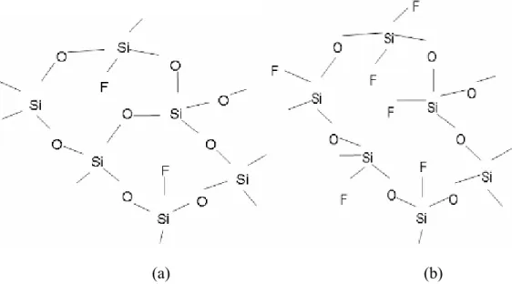
Terminal Si-F bond broke silicon oxide network structure as shown in Figure 2.10 and decreased the density of FSG film, which in turn the dielectric constant. The dielectric constant of FSG was also dependent on fluoride concentration. When concentration of fluoride increased, the dielectric constant decreased. However, FSG cannot stand in high temperature at which FSG released HF to react with Ti, Ta, TiN to form fluoride or volatile SiF4 species. Therefore, the operating temperature of
backend processing steps must be kept under 450 oC. In addition, too many Si-F bonds would also result in increased moisture adsorption
(a) (b)
Figure 2.10 Chemical structure of fluorinated silicate glass at (a) low fluorine concentration and (b) high fluorine concentration
2.4.1.b Carbon-doped oxide (CDO)
The chemical structure of carbon-doped oxide (CDO) was shown in Figure 2.11, in which the incorporation of Si-CH3 terminal groups reduced the polarizability of
SiO2, thus lowered the dielectric constant.
Figure 2.11 Chemical structure of carbon-doped oxide (CDO)
Generally, there were two kinds of precursors. One contained oxygen in the chemical structure such as tetramethylcyclotetrasiloxane (TMCTS)[17], octamethlycyclotetrasilane (OMCTS) [18], dimethyldimethoxysilane (DMDMOS) [19], and methyltrimethoxysilane (MTOS) [20]; the other had no oxygen such as methylsilane (1MS), dimethylsilane (2MS), trimethylsilane (3MS) [21,22], and tetramethylsilane (4MS). These chemical structures were shown in Figure 2.12.
Si H CH3 H H Si H CH3 H3C H Si H3C CH3 H CH3 Si H3C CH3 H3C CH3 1MS 2MS 3MS 4MS Si O Si O Si O Si O CH3 H H H3C H H3C H CH3 Si O Si O Si O Si O CH3 H H H3C H H3C H CH3 Si H3C OCH3 H3C OCH3 Si H3C OCH2CH3 H3C OCH2CH3 DMDMOS DEMS TMCTS OMCTS Si OCH3 H3CO CH3 H3CO MTOS
Figure 2.12 Chemical structures of precursors for carbon doped oxide
When 1MS, 2MS or 3MS were used as CDO precursors, the CDO deposition process needed oxygen or N2O as an oxidant to oxidize precursors. Dielectric constant of
CDO was about 2.6~3.3 which depended on the amount of methyl groups. In general, the amount of increased methyl groups could reduce dielectric constant of CDO.
However, too many methyl groups themselves as terminated group would also reduce mechanical strength.
The representative film properties of COD and SiO2 films were summarized in Table
2.3 [18]. Since the thermal expansion coefficient of CDO was close to copper (Cu) and titanium nitride (TiN), CDO was compatible for copper integration. The commercial CDO materials such as CORALTM were from Novellus Inc., Black DiamondTM from Applied Materials Inc. and AurouaTM from Tokyo Electron Inc. [23~25]
Table 2.3 Film properties of carbon-doped oxide and PECVD SiO2 [18].
Property CDO PECVD SiO2
Dielectric constant < 3 4.2
Refractive index <1.42 1.46
stress Tensile Compressive
Young’s modulus <10 GPa 70~80 GPa
Hardness <2 GPa 7~9 GPa
Density <1.4 g/cm3 2.2 g/cm3
Thermal conductivity <0.4 W/mC ~1 W/mC
CTE <10 ppm/oC <1 ppm/oC
2.4.1.c Hydrogen silsesquioxane (HSQ)
Empirical formula of silsesquioxane was (RSiO1.5) n [26], where R was aromatic
group, alkyl group or hydrogen. The procedure for the preparation of silsequioxane materials was shown in Figure 2.13. First step was hydrolysis of monomers, in which haloid or alkyloxy group was converted into hydroxyl groups. Then monomers went
through polycondenation with hydroxyl groups to become a larger molecule. Finally, the oligomers, which covered high molecular weight, would be cured at high temperature. However, the final product contained T8, T10, and T12 [27] structure which was dependent on the reaction condition, as illustrated in Figure 2.14.
Step 1 : Hydrolysis
X : Cl, OCH
3or OCH
2CH
3R Si X X X H+ H2O R Si OH X OH H O Si R HO Si HO R OH n O Step 2 : Polycondensation H O Si R OH Si OH R OH n OH -H O Si R Si HO OH H O Si OH Si R OH n O O O O Step 3 : Crosslink Si O Si O Si O Si OH O Si O Si O O Si O R R R O R CH3 O O O Si O O R Si R O Si O O O O Si O O O Si O O O m n Si R n H O Si R Si HO OH H O Si OH Si R OH n O O O O Cage Network
Figure 2.13 Silsesquioxane preparative pathways [28].
When R was hydrogen, the silsesquioxane was called hydrogen silsesquioxane as shown in Figure 2.15.a. Hydrogen silsesquioxane (HSQ) contained cage structure
which had larger free volume than silicon dioxide network structure. Hydrogen attaching on Si atom reduced its poarizability. This is the reason why HSQ had low dielectric properties. However, Si-H bond was sensitive to oxygen. If oxygen existed during the curing process, Si-H bond would convert to Si-OH bond, making HSQ become more hydrophilic. In curing process, temperature was also an important parameter. The modulus and hardness would increase since high curing temperature made cage structure convert to network structure [29]. However, increasing curing-temperature would degrade dielectric properties.
2.4.1.d Methyl silsesquioxane (MSQ)
[28]
When R was methyl group, the final product was called methyl silsesquioxane (MSQ) which was shown in Figure 2.15.b. [28]. MSQ synthesis commonly used methyltrimethoxysilane (MTOS) illustrated in Figure 2.12, as monomer, whose reaction steps were illustrated in Figure 2.13. The reason why dielectric constant of MSQ was lower than HSQ was that polarization of methyl group attaching on Si atom was lower than hydrogen and methyl group, which had larger free volume. Si-CH3
bond was more stable than Si-H, and therefore MSQ thermal stability and chemical resistance were greater than HSQ. Tables 2.4 listed the key materials properties of HSQ and MSQ.
Figure 2.14 (a) ladder structure, (b)~(d) cage structure of T8, T10, T12[27] Si O Si O Si O Si OH O Si O Si O O Si O H H H O H CH3 O O O Si O O R Si R O Si O O O O Si O O O Si O O O m n Si
H
HSQ
a
Si O Si O Si O Si OH O Si O Si O O Si O H3C CH3 CH3 O CH3 CH3 O O O Si O O R Si R O Si O O O O Si O O O Si O O O m n Si
CH3
MSQ
b
Figure 2.15 Chemical structures of (a) HSQ and (b)MSQ
Table 2.4 Key material properties of HSQ and MSQ [29]
Property HSQ MSQ
Dielectric constant 3 at 1MHz 2.8 at 1MHz
Modulus 6 GPa 3~5 GPa
Density 1.4~1.5 g/cm3 1.2~1.3 g/cm3
Tensile strength 80 MPa 50 MPa
2.4.2 Organic-based low-k polymeric dielectrics
2.4.2.a SiLK
TMSiLKTM was developed by Dow Chemical Company in 1996. SiLKTM was a solution of low molecular weight aromatic thermosetting polymer (polynaphthalene)
[30]. Dielectric constant of SiLKTM was about 2.65, and it also had good gap filling,
mechanical strength and good thermal stability. In April 2000, IBM announced SiLKTM could be commercially fabricated in copper dual damascenece backend structure in IC devices [26]. The properties of SiLKTM were summarized in Table 2.5.
Table 2.5 Summary of SiLKTM properties [30] Property Value Dielectric constant 2.65 Leakage current at 1MV/cm 4 MV/cm Refractive index 1.63 Moisture uptake at 20OC RH 80% 0.24 % Thermal stability >425 oC Weigh loss at 450OC 0.7 wt%/hr Thermal conductivity 0.19 W/ mk at 25oC Glass transition >490oC Young’s modulus 2.45 GPa
Strength 90 MPa
Ultimate strain 11.5 %
Hardness 0.38 GPa
Toughness 0.62 MPa m
Residual stress at RT 56 MPa
CTE 66 ppm/oC
However, the implementation of SiLKTM IBM suffered a temporary setback in
April, 2004 due to reliability issue caused by the unexpected, large coefficient of thermal expansion (CTE) mismatch at high temperatures (300-400 oC), until a
modified version SiLK DTM was introduced later in 2004. [31]
2.5 Porous low-k materials
The dielectric constant of production-worthy, dense dielectric materials was limited to 2.5-2.6. In order to achieve lower dielectric constant, incorporation of pores into dielectrics matrix was necessary and essential. Pore, introduced into matrix, could
methods to produce porous materials: (1) Sol-Gel method, (2) Nano-clustering method, and (3) Templating method, which would be described briefly below:
(1) Sol-Gel method
Sol-Gel method [32] was a synthesis process of solid materials. The precursor commonly had a metal or Si in center such as Al(OH)4, tetramethyloxysilane, which
included –OH as reactive groups. The first step was poly-condensation of precursor forming colloids, and colloids dispersion in liquid solution or solvent. Then particles continuously reacted with others which formed three-dimension network structure as schematically illustrated in Figure 2.16.
Time condensation colloids 3-D sturcture dry final product
a
b
c
Figure 2.16 Sol-Gel processes (a) Sol, (b) Gel, (c) SEM picture of aerogel [33]
During the aging stage, the gel network became stronger. In drying process, the liquid in pore was replaced with gas or air. The gel could be dried with two main methods called aerogel and xerogel [32]. Aerogel referred to the gel, which was obtained when the liquid in pore was removed by supercritical drying. The network remained unchanged. Xerogel referred to drying by conventional or ambient drying. The sol-gel
method was difficult to control pore size of the prepared porous materials.
(2) Nano-clustering (NCS) method
The pore formation method for NCS was schematically illustrated in Figure2.17
[34]. The silica monomers were hydrolyzing by the compounds and silica which aggregated into a small size cluster in a solution. After spin coating, the nano-clusters polymerized during the subsequent curing process.
Figure 2.17 Schematic illustratration of pore formation in nano-clustering silica[34]
(3) Template method
Porous low-k dielectrics with high porosity and ordered pore geometry could be prepared by self- assembly surfactant template method, as illustrated in Figure 2.18. The porosity and pore size could was controllable by adjusting molecular size or template agent loading. The microstructure of template materials could be ordered or disorder with lamellar, cubic or hexagonal structure [35-41].
Figure 2.18 Pore was formed by thermally or chemically removing templating agent or porogen.
Examples of ordered and disordered structure reported in literature were illustrated in Figure 2.19. [35-41]
Figure 2.19 Ordered and disordered phases of microstructured materials [35-41].
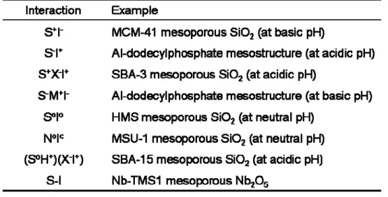
The formation of these microstructure involved surfactant (S)/inorganic (I) interaction. The interaction include electrostatic, (S+I-, S-I+, S+X-I+, S-M+I-)[42-45], hydrogen bonding (S0I0, N0I0)[46,47], hydrogen bonding/electrostatic [(S0H+)(X-I+)][48,49] and covalent (S-I) [50]. Various surfactant(S)/inorganic(I) interaction and examples were in Table 2.6. For example, MCM-41 and M41S [42,43] materials were synthesized
by S+I- interaction under basic condition. The interaction between the cationic ammonium surfactant (S+) and the hydrated silica (I-) led to formation of hexagonal array. However, ionic and neutral amine surfactant were typical toxic and expensive, and impractical for used in IC industries.
Table 2.6 Various surfactant(S)/inorganic(I) interaction and examples including PH condition
The nonionic amphiphilic surfactants including di-block and tri-block copolymers were relatively low cost, nontoxic and biodegradable [51]. Amphiphlic block copolymers (ABC) had hydrophilic and hydrophobic segment, and the pore size could be controlled by adjusting molecular weight or number of repeating unit.In this thesis, amphiphlic block copolymers (ABC) were employed as high-temperature porogens in the low-k methylsilsesquioxane (MSQ) matrix, which would be further described in details in Chapter 3.
2.6 Impact of porous materials on IC integration
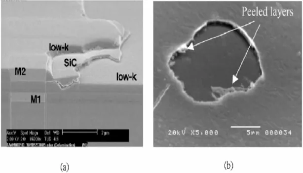
Comparing to traditional silicon dioxide, porous materials possessed weaker mechanical properties and chemical resistance. Weak mechanical properties led to failure in the interconnect; for example, (1) the delamination of multilayer structures during chemical mechanical polish (CMP) process [52] as shown by Figure 2.20(a), and (2) the peeling or delamination of low-k layer during wire bonding as shown by Figure 2.20 (b) [53].
Figure 2.20 SEM photographs of (a) delamination during CMP process and (b) delamination and failure after wire bonding
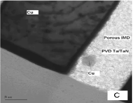
Since etching rate of porous materials was faster than dense materials, the surface of porous materials would be rougher than that of the dense one after etching process. The non-continuous sidewall or open pores on the sidewall surface would make the barrier precursor penetrate into dielectrics so that the barrier could not prevent copper diffusion into dielectrics [55] as illustrated in Figure 2.21. Penetration of copper or barrier precursor, into dielectrics would cause degradation of electric
properties, such as increasing leakage current and decreasing breakdown voltage. Degradation of those electric properties could lead to circuit failure. To circumvent non-continuous sidewall issue, pore-sealing methods had been proposed. Two examples of pore-sealing were described below:
Figure 2.21 Penetration of copper into non-continuous sidewall of a porous dielectric
(1) Plasma pore sealing
Plasma pore sealing [55, 56] was utilized which the bombardment made the
surface of porous films dense. The formation of thin layer on pore at sidewall prevented penetration of precursor into the dielectrics.
(2) Deposition of a thin layer on surface
Z. Chen et al [57], C. Jwzewski et al [58], and V. Jousseaume [59]
demonstrated that effective pore sealing method could be achieved by applying a thin low dielectric layer such as SiC:H between the barrier and porous low-k, as shown in Figure 2.22 (a), to improve the non-continues sidewall. This sealing method was schematically illustrated in Figure 2.22 (b).
Figure 2.22 (a) TEM image of sidewall profile after pore sealing by a thin low dielectric layer [54] , (b) The schematic diagram of sealing concept [59]
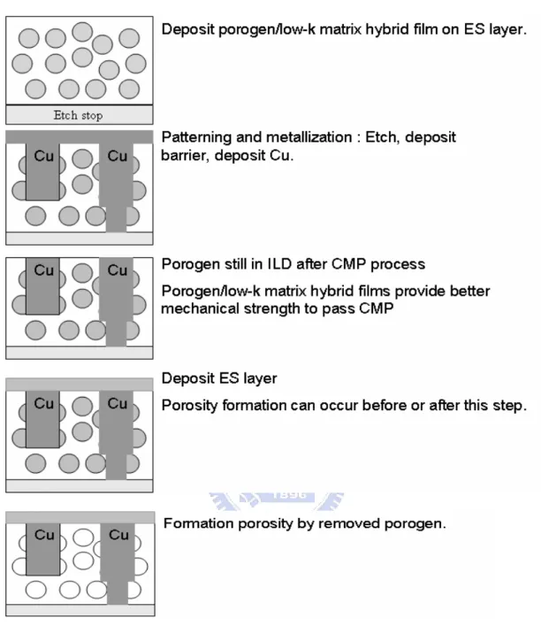
However, the above-mentioned pore sealing required additional steps, such as thin layer and removal of such layer in via area, which incurred extra cost and reliability concern. Therefore, Shipey Company proposed a Solid-FirstTM [60] scheme
to circumvent non-continuous sidewall issue, which was schematically shown in Figure 2.23. The first step of conventional porous low-k materials was to create pores at or immediately after deposition, but Solid FirstTM scheme was to defer the removing of template agent or porogen in the final step, i.e. at the completion of a Cu/low-k layer. The sequence of Solid-FirstTM process included (1) low-k film containing high temperature porogen was deposited, (2) patterning steps (lithography, etch, and clean), (3) metallization and CMP, and then (3) removal of high temperature porogen at 300-450 oC. The high temperature porogen (template agent) must possess high thermal stability for T > 300-350 oC commonly used in the backend processing steps..
Recently, Che et al. demonstrated porous ultra low-k materials (k~2.0) with poly styrene-block-4-vinylpyridine (PS-P4VP), an amphiphilic block copolymer (ABC), as a high-temperature porogen in the Solid-FirstTM scheme[5]. The modulus of hybrid films below the critical porogen loading (< 30%) could pass chemical-mechanical polish (CMP) test (> 4.0 GPa). Thus, Solid-FirstTM could solve not only the problem of non-continuous sidewall but also the low mechanical strength of porous films [5].
2.7 Impact of moisture on low-k materials.
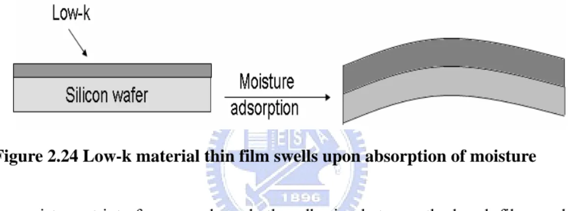
Most low-k films had relative high coefficient of thermal expansion (CTE) compared to silicon substrate so that those films exhibited tensile stress. Water in films would reduce fracture resistance. By combining tensile stress with worse fracture resistance, low-k films with moisture uptake tended to crack [61]. Moreover, moisture adsorption made the low-k polymer swell, and thus increased the tensile stress as illustrated in Figure 2. 22.
Figure 2.24 Low-k material thin film swells upon absorption of moisture
The moisture at interface may degrade the adhesion between the low-k films and cap layer [62]. In addition, the moisture outgassing may destroy the diffusion barrier or etch-stop layer during thermal process [63] as illustrated in Figure 2.23
The dielectric properties of porous low-k materials would be significantly degraded if residual H2O (Kwater = 78) was adsorbed into the matrix and porogen.
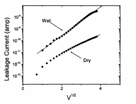
Water, in porous low-k films, also provided leakage path to lead to increasing leakage current and decreasing breakdown voltage as illustrated in Figure 2.24 [64, 65]. Thus, adsorption of moisture in low-k materials would reduce time dependent dielectric breakdown (TDDB) lifetime.
Figure 2.26 Leakage current of low-k thin films under wet and dry conditions
The mount of moisture adsorption of polar surface would be expected larger than non-polar surface, since high polarity of surface could induce multilayered adsorbents by long-range force such as Van der Waals force. For example, nanoporous silica xerogels contained unreacted hydroxyl (-OH) groups on surface that made the amount of moisture adsorption larger than that after the elimination of –OH groups of silica by HMDS treatment or TMCT treatment [66, 67], and high surface area could provide more sites for adsorbents as shown schematically in Figure 2.27 [67].
Figure 2.27 Schematic diagramd of water adsorption onto SiO2 with and without HMDS treatment [64].
In summery, we realized that integration of porous low-k materials had following reliability problems.
(1) Low mechanical strength cannot pass CMP process.
(2) Low chemical resistance led to corrosion or etch happen during wet cleaning. (3) High surface area resulted in high moisture uptake and moisture outgassing made
delamination of multilayer structure occur.
(4) Bias-temperature stressing (BTS) failure due to non-continuous sidewall coverage of barrier.
In order to circumvent non-continuous dielectric sidewall, Shipey Company proposed a Solid-FirstTM approach that was the formation of porous dielectric after the completion of a metal layer, and then thermally removed the sacrificial high-temperature porogen. However, there was little understanding of moisture uptake about dielectrics, especially the porogen/low-k matrix hybrid films. During the integration process the dielectric films existed in the form of porogen/low-k matrix
process which contained a lot of water. Hence, the analysis of porogen/low-k matrix films and porous films on moisture uptake aspect was important.
It has been well known that quartz crystal microbalance (QCM) was a powerful tool to weight very small mass load in nano-gram scale. In this thesis, we employed QCM to characterize the moisture uptake and diffusion behaviors of low-k materials.
Chapter 3 Experimental
This chapter described the experimental methods and steps, including low-k precursor solution preparation, spin coating, thermal processed, quantitative measurement of moisture uptake in low-k films by quartz crystal microbalance, and collection of chemical bond information by FTIR, thickness and refractive index by n&k analyzer, pore morphology by SEM, and dielectric constant by CV-dot measurement. Flow-chart of experimental procedures was summarized in Figure 3.1
Figure 3.1 Flow-chart of experimental procedures Precursor solution
Coating
QCM: (coating on quartz crystal)
To compare the moisture uptake with different samples and the diffusion
Hybrid film on wafer
Porous film on wafer HMDS Modified porous films on Al/wafer Al electrode C-V (MIS structure): To compare the dielectric constant under different
relative humidity.
N&K
3.1 Preparation of low-k films
3.1.1 Chemicals
(1) Polymethylsilsesquioxane (MSQ) as low-k matrix.
MSQ, CAS No.68554-70-1, purity ≥95%, product by Gelest Inc.
(2) High-temperature porogen was used as a template which was removed after the completion of a metal/low-k layer in the Solid-FirstTM scheme
(a)
Polystyrene-block-poly(4-vinylprydine) as high-temperature porogen PS-b-P4VP, 10% PS,CAS No.26222-40-2, Product by Sigma-Aldrich Co.(b) Polystyrene-block-polybutadiene-block-polystyrene as high-temperature porogen
(3) n-Butanol as solvent.
CAS No.71-36-3, purity: ≥99.4, product by Scharlau
HO
(4) Tetrahydrofuran as solventTHF, CAS No.109-99-9, purity≥99.9, product by ECHO
O
(5) Hexamethlydisilazane(HMDS) used as hydrophobic modifying agent, which was obtained from Sigma-Aldrich Co.
NH
Si
Si
CH
3CH
3H
3C
CH
3CH
3CH
33.1.2 Preparation of low-k precursor solution
Methylsilsesquioxane (MSQ) was dissolved in n-butanol to form a 5 wt% solution which solution was as precursor of dense MSQ films.For hybrid films and porous films precursor, MSQ was first dissolved in solvent, and then high-
temperature porogen was mixed at various loadings to form a 5 wt% solution. The solvent of PS-PB-PS and PS-P4VP was tetrahydrofuran (THF) or n-butanol.
3.1.3 Deposition of low-k films
Before spin coating,the solution was initially filtered through a 0.2 µm PTFE filter (Millipore Inc.) in another bottle, and then placed in an ultrasonic bath for 1 minute as shown in Figure 3.2, to ensure no bubble in the solution. The precursor was spin coating onto silicon wafer or AT-cut quartz crystal (9 MHz resonant frequency, from Mercury ElectronicCompany). The dense, hybrid, and porous low-k films were prepared using different thermal process described in detail below.
(1) Preparation of dense polymethylsilsesquioxane (MSQ) films at 250 oC and 400 oC
The methylsilsesquioxane (MSQ) precursor was spin coating onto silicon wafer
or AT-cut quartz crystal, and then cured at 250oC for 30 minutes for comparative study with the corresponding MSQ/porogen hybrid films at the same temperature (250 oC). This film was further cured at 400 oC for 60 minutes in a quartz tube furnace to be used as the control, dense low-k.
(2) Preparation of MSQ/porogen hybrid films
The solutions with various high-temperature porogen loadings were spin coating onto silicon wafer or AT-cut quartz crystal with, and then cured at 250oC for 30 minutes.
(3) Preparation of porous films
Precursors were spin coating onto silicon wafer and AT-cut quartz crystal, and then cured at 250 oC for 30 minutes. Then, the high-temperature porogen was removed at 400 oC for 60 minutes in quartz furnace
The porous low-k films on quartz and wafer of (3) were placed inside a Pyrex container and treated with saturated HMDS vapor under 70oC for 24 hours. Prior to the introduction of HMDS, low-k film was purged at N2 at high flow rate to ensure low moisture adsorbed on the surface.
Figure 3.2 Schematic illustration on the preparation of precursor solution
3.2 Experimental techniques
3.2.1 n&k analyzer
The n&k analyzer 1200 was used in this study to obtain refractive index (n) and film thickness (d) information of low-k films. The experimental steps were listed below:
1. To scan standard sample as a baseline. (The wavelength ranged from 190 nm to 900 nm.)
2. To put sample wafer upside down on the n&k analyzer, and then scan again to collect the typical experimental curve illustrated in Figure 3.3.
The experimental curve was fitted using Forouhi-Boomer Dispersion relation [68] (Equation 3.1) to deduce refractive index (n) and film thickness (d).
∑
=−
+
+
+
∞
=
q i i i i iC
E
B
E
C
E
B
n
E
n
1 2 0 0)
(
)
(
………..(3.1) where ⎥ ⎦ ⎤ ⎢ ⎣ ⎡ + − + − = B E B E C Q A B g g2 2 0 2(
)
⎥⎦⎤ ⎢⎣ ⎡ + − = E C B E C Q A C g 2 g 2 2 0(
)
2 1 2 4 2 1 B C Q= −E:Incident energy of light
B, C:Parameter which relate to electron structure of materials q:number of terms
n(∞) > 1
3.2.2 Specular reflectance Fourier-transform infrared spectroscopy
(FT-IR)
FTIR has been extensively applied to qualitative analysis of organic
compounds due to the specific absorption wavelength by different vibration and rotation modes in the infrared wavelength range. The S/N ratio was very small for thin film measurement using transmission mode. Therefore specular reflectance FTIR apparatus VeeMAX [69] and PIKE 100 FTIR from PIKE Technologies Inc were employed for thin film characterization in this thesis.
The specular reflectance FTIR was schematically illustrated in Figure 3.4. The thin film samples were spun onto Al/silicon wafer substrate, where Al thin film was used as a reflective mirror. The spectrum was collected in 500~4000 cm-1 range at a resolution of 2 cm-1 and 30o incident angle.
Figure 3.4 Schematic diagram of a specular reflectance infrared speectroscopy
3.2.3 Capacitance measurement
Metal-insulator-semiconductor (MIS) sample was used for measuring the dielectric properties. The fabrication steps of MIS samples were illustrated in Figure 3.5 and described below:
1. To deposit low-k materials on a p-type (100Ωcm) silicon wafer and cure the film
Sample film
at 250℃.
2. Al thin film (5000 A) to serve as an electrode, was then deposited onto dielectric film, which was covered with a shadow mask with various dot sizes as shown in Figure 3.6
The capacitance of low-k film in MIS structure was measured by a HP-4280 C-V meter. The capacitance value was then substituted into Equation 3.2, to obtain the dielectric constant (k).
d
A
K
C
=
ε
0 ……….(3.2) C : capacitanceε0 : Permittivity of free space, 8.85419 x 10⁻¹² C2/Jm
A : electrode area d : dielectric thickness k : dielectric constant
Figure 3.5 The process flow for fabricating a MIS sample for CV-dot measurement
Figure 3.6 Shadow mask with three different diameters for CV-dot measurement
Electrode area and thin film thickness were two major sources of error in the dielectric constant measurement. In order to eliminate such measurement errors, linear curve fitting of capacitance versus area for various dot sizes was shown in Figure 3.7. Then the fitted value of slope was substituted into Equation 3.2 to obtain the dielectric constant.
Figure 3.7 The utilization of linear curve fitting of various dot sizes to minimize the errors from fringes effect and area measurement
3.2.4 Dual beam (focused ion beam & electron beam) System
(FIB/SEM)
Topography of porous low-k films was observed by FEI Nova 200 Dual beam, focused ion beam and electron beam System (FIB/SEM). The ion beam focused by electromagnetic lens to cut and etch in very small dimension. General ion beam used liquid metal Gallium (Ga) ion source, which had low melting point, low vapor pressure and large resistance of oxidation. Typical FIB system consisted of liquid metal source, electromagnetic lens, second ion detector, scanning electrode, X-Y-Z sample stage, and vacuum system schematically illustrated in Figure 3.8.
Figure 3.8 Schematic diagram of a FIB/SEM system
Liquid metal ion was extracted by electric field and through automatic variable aperture (AVA) to adjust the spot size. The FEI Nova 200 Dual beam system offered a function of not only focus ion beam but also electron beam. During ion cutting or etching, electron beam serviced as image probe (SEM) that precisely controlled cutting or etching process.
3.2.5 Quartz Crystal Microbalance (QCM)
Theory of Piezoelectric Quartz crystal microbalanceIn Chapter 2 we realized that the dielectric properties of porous low-k materials would be significantly degraded if residual H2O (kwater~78) adsorbed in the matrix and
porogen. In addition, the moisture outgassing may cause delamination or catastrophic failure at low-k/diffusion barrier or low-k/etch-stop interface during the temperature
low-k films, especially in different stages of Solid-FirstTM scheme, was important to devise the processing condition in order to eliminate catastrophic failure. In this study, a home-built quartz crystal microbalance (QCM) was employed tomeasure moisture uptake of low-k films. QCM was an extremely sensitive tool down to nano-gram level due to the application of piezoelectric effect. The quartz crystal would deform and had a specific resonant frequency while AC electronic filed was applied to quartz crystal. According to Sauerbrey equation [70], the mass load on crystal could be calculated by the measured resonant frequency. The quartz resonator was first explored by Sauerbrey, whose equation could be deduced as follows.
Sauerbrey Equation [70]
For a quartz crystal plate to oscillate in thickness shear mode, the following equation must be satisfied:
2
q
tq= λ ………(1)
tq : thickness of the crystal
λq : wavelength of shear-mode elastic wave
Speed of acoustic wave in the same material was a constant and could be described by the following equation:
2 1 ⎟⎟ ⎠ ⎞ ⎜⎜ ⎝ ⎛ = q q v ρ μ ………(2) ν: wave speed
μq : the shear modulus of crystal ρq : the density of crystal If ν=f0 λ substitute into (1), then
tq f 2 0 ν = ………(3)
Assume a thin layer with thickness, △t, was absorbed, then
t tq q Δ + = 2 λ
After adsorbed, wavelength became longer and wave speed would not change, we can get following equation:
tq t f =−Δ Δ ………(4) Substitution of (3) into (4) 2 1 0 0 0 ⎟⎟ ⎠ ⎞ ⎜⎜ ⎝ ⎛ Δ − = − = Δ q q t f f f f ρ μ ν ………(5)
Assume density of adsorbed layer equal to quartz crystal
q t A m= Δρ
Δ ………(6)
A : piezoelectric active area △m : mass of adsorbs Substitution of (6) into (5) ⎟⎟ ⎟ ⎟ ⎠ ⎞ ⎜⎜ ⎜ ⎜ ⎝ ⎛ Δ − = Δ 2 0 2 f f A m ρqμq ……… Sauerbrey Equation (3.3)
ρq: the density of crystal (~2.648 g.cm3)
A: piezoelectric active area
△f: Frequency change before and after adsorption △m: Mass loading
Quartz crystal microbalance (QCM) system
A home-built quartz crystal microbalance system, schematically illustrated in Figure 3.7, consisting of vacuum chamber, oscillator, frequency counter (HP 53131A), temperature controller, water vapor bubbler and computer-controlled data collection system, was used in this thesis. The AT-cut quartz crystal with 9 MHz resonant frequency (Mercury Electronics. Inc.) had a diameter and thickness of 0.8 cm and 200 μm, respectively. Diameter of active Au electrode was 0.4 cm. The measurement of moisture uptake was carried out under 100% relative humidity at 30 oC. The sensitivity of our QCM using a 9 MHz AT-cut quartz crystal is 1.72 ng/cm2 based on the 1 Hz resolution of HP frequency counter according to Sauerbrey equation.
Sample preparation and moisture uptake measurement using QCM
Procedures of sample preparation and QCM system moisture uptake measurement were listed below:
1. Prior to the deposition of low-k film, crystal resonant frequency (f0) was measured
and recorded in the vacuum chamber.
2. Low-k precursor solution was spin coating onto a quartz crystal at a specific speed to obtain 0.5μm thickness. Caution was taken to mask area excluding the top-side Au electrode using a tape to prevent poor electric contact caused by the contamination of precursor solution.
described in Section 3.1.3.
4. After curing, the low-k/quartz sample was placed into a QCM holder within the vacuum chamber. After the chamber was evacuated, a stable frequency value for low-k/quartz, called f1 was measured and recorded.
5. When the water bubbler reached 100% saturation steady-state at 30 oC, the saturated moisture was introduced into the chamber to start adsorption process and
in-situ measurement of resonance frequency as function of time through a computer-controlled data collection system as illustrated in Figure 3.10. The resonate frequency of quartz crystal decreased due to mass load on thin film when moisture was adsorbed in the low-k/quartz sample. As the adsorption of moisture reached steady state, a stable frequency value, called f2, was recorded as shown in
Figure 3.10.
6. Afterwards, the frequency was further monitored as function of time during the desorption process under pump down. Then, the stable frequency, called f3, was
recorded to check if moisture was fully desorbed or any chemical change if f3 ≠ f1.
7. From the previous steps, amount of moisture uptake in low-k film could be calculated from △f = f1-f2 through Sauerbrey Equation. In this thesis, moisture
uptake was expressed in term of wt%, i.e. (f1-f2)/( f0-f1)x100% as illustrated in
Figure 3.11.
8. Moisture uptake of low-k/quartz sample after HMDS treated measurement was the same as low-k/quartz sample.
oscillator Frequency
counter computer IEEE488GBIP
Vacuum pump Vapor source
Temperature controller
Figure 3.9 Schematic diagram of QCM system for moisture uptake measurement
RH 100%, 30oC
0
500
1000
1500
2000
8993440
8993460
8993480
8993500
8993520
8993540
8993560
8993580
F
requency (Hz)
Time (sec)
sorption
Vaccum
desorption
Figure 3.10 The frequency change of the crystal resonator at 30 oC versus time during sorption and desoprtion for MSQ/PS-P4VP (10wt%) hybrid film
![Figure 2.3 Relationship between generation node and RC-delay in gate and interconnect for Al/SiO2 and Cu/lok k [9]](https://thumb-ap.123doks.com/thumbv2/9libinfo/8399377.179145/20.892.141.751.126.466/figure-relationship-generation-node-delay-gate-interconnect-sio.webp)
![Figure 2.8 Relationship between dielectric constant and applied electric filed frequency [12]](https://thumb-ap.123doks.com/thumbv2/9libinfo/8399377.179145/26.892.141.731.112.418/figure-relationship-dielectric-constant-applied-electric-filed-frequency.webp)
![Figure 2.17 Schematic illustratration of pore formation in nano-clustering silica [34]](https://thumb-ap.123doks.com/thumbv2/9libinfo/8399377.179145/39.892.138.753.370.655/figure-schematic-illustratration-pore-formation-nano-clustering-silica.webp)