國
立
交
通
大
學
電機學院 IC 設計產業研發碩士班
碩
士
論
文
奈米互補式金氧半製程下之低漏電電源箝制
靜電放電防護電路
LOW-LEAKAGE POWER-RAIL ESD CLAMP
CIRCUIT IN NANOSCALE CMOS TECHNOLOGY
研 究 生:邱柏硯
指導教授:柯明道 教授
奈米互補式金氧半製程下之低漏電源箝制
靜電放電防護電路
LOW-LEAKAGE POWER-RAIL ESD CLAMP
CIRCUIT IN NANOSCALE CMOS TECHNOLOGY
研 究 生:邱柏硯 Student:Po-Yen Chiu
指導教授:柯明道 Advisor:Prof. Ming-Dou Ker
國 立 交 通 大 學
電機學院 IC 設計產業研發碩士班
碩 士 論 文
A Thesis
Submitted to College of Electrical and Computer Engineering National Chiao Tung University
in partial Fulfillment of the Requirements for the Degree of
Master in
Industrial Technology R & D Master Program on IC Design
July 2008
Hsinchu, Taiwan, Republic of China
奈米互補式金氧半製程下之低漏電電源箝制
靜電放電防護電路
學生:邱柏硯 指導教授: 柯明道 教授
國立交通大學電機學院產業研發碩士班
摘 要
本篇論文主旨在設計奈米互補式金氧半製程下之低漏電電源箝制靜電放電 防護電路。其原理為利用電路和元件特性,使電路整體漏電降到最低,但又能具 有高水準之靜電放電防護能力。本篇論文分為三大部分,主要透過電路模擬以及 實驗的量測來驗證所提出的新型設計。 第一部分是在介紹關於研究穿隧現象(Gate-Tunneling)的演進過程,爾後互補 式金氧半製程中,隨著閘極氧化層越薄的情況下此現象有越明顯的趨勢。在過去 的研究中已經研究出此穿隧現象(Gate-Tunneling)的機制和相對應之方程式,並且 建設穿隧現象(Gate-Tunneling)的模型,應用在先進製程之奈米互補式金氧半製程 裡。 第二部份為應用 65 奈米互補式金氧半製程薄氧化層元件模擬,除了模擬 MOS 電容閘極漏電的現象之外,之後再進一步探討此種 MOS 電容應用在傳統電 源箝制靜電放電防護電路和新型電源箝制靜電放電防護電路中,MOS 電容嚴重 漏電對整體電路的影響。在模擬結果中傳統電源箝制靜電放電防護電路因 MOS 電容漏電的影響,帶來更嚴重的漏電問題。雖然有其他電路方法解決電路漏電問 題,但是還是存在著漏電路徑經由 MOS 電容,此漏電數量還是非常嚴重。此提 出新型設計目的就是為了解決漏電問題,在正常的工作下不會有大量漏電的問題,並且在靜電放電轟擊之下亦能適時動作排放靜電放電電流,在模擬結果中此 新型的設計是可行的並且具有相當低的漏電流。 第三部份為實際量測結果,所有電路和元件皆以 65 奈米互補式金氧半製程 實現,實驗結果顯示,閘極漏電流的問題已經不能忽略,傳統電源箝制靜電放電 防護電路受到 MOS 電容漏電的影響,有著更嚴重的漏電問題(室溫下約六百一 十三微安培),必須要有所改善。此新型電源箝制靜電放電防護電路可以達到所 需的要求,除了有極低的漏電流(室溫下約一百一十六奈安培)之外,亦有非常好 的靜電放電防護能力,在人體放電模式靜電放電轟擊超過八千伏特,並且在機器 放電模式的靜電放電防護能力約七百五十伏特。
LOW-LEAKAGE POWER-RAIL ESD CLAMP
CIRCUIT IN NANOSCALE CMOS TECHNOLOGY
Student: Po-Yen Chiu
Advisor: Prof. Ming-Dou Ker
Industrial Technology R & D Master Program of
Electrical and Computer Engineering College
National Chiao Tung University
ABSTRACT
The aim in this thesis is to design the low-leakage power-rail ESD clamp in nanoscale CMOS technology. The principles are using circuit and component characteristics to minimize leakage of the circuit. Besides having the lowest leakage current, it also can have high robustness of ESD protection. This thesis includes three topics; the main parts are through the circuit simulation and experimental measurements to verify the new proposed design.
The first part is to introduce the evolution of gate-tunneling research. With the gate-oxide thickness become thinner and thinner in CMOS processes, the phenomena become more and more serious. In the past research, the mechanisms and formulas of gate-tunneling have been observed. The model of gate-tunneling also has been applied into advance CMOS processes.
The second part is to simulate circuits and components in the 65-nm CMOS process with thin-oxide devices. Besides simulating the leakage current of MOS capacitor, the further discusses are what it will influence if MOS capacitor is applied to traditional power-rail ESD clamp circuits and new proposed power-rail ESD clamp circuit. In the simulation results, the leakage of MOS capacitor causes incorrect function which causes another leakage path and leak more current in the circuit. Although there have other methods to reduce the leakage current, but there is still
have a leakage path through MOS capacitor. However, with a voltage drop across MOS capacitor, the MOS capacitor always leaks some current. The leakage current is still very huge. The new proposed design was designed to have lower leakage current when it is under normal circuit operating conditions and discharge ESD current in time when it is under ESD transient. As the simulation result, the new proposed design has lower leakage current than traditional designs.
The third part is measured results. In this thesis, a new low-leakage power-rail ESD clamp circuit designed with the consideration of gate-leakage issue has been proposed and verified in 90-nm and 65-nm CMOS processes. According to the measured results, the gate leakage issue needs to be taken into consideration. The traditional designs have more leakage current because the leakage of MOS capacitor, so the traditional designs can not be used if it is implemented in nanoscale CMOS process with thin-oxide device. The new proposed design has the lowest leakage current (228 nA at 25 oC) and good robustness of ESD tests. It has ESD robustness of over 8 kV in HBM and 750 V in MM.
Acknowledgment
首先要感謝的是我的指導教授柯明道博士,感謝老師這兩年來的教導和鼓 勵,到現在我心中還未忘記當初老師收我進入實驗室的喜悅,當然的這份喜悅會 繼續跟隨著我接下來的博士班生涯。學生資質駑鈍,感謝老師一路上不厭其煩的 給予指導,不僅在專業知識的學習,另外在做人處事方面亦有相當的收穫。接下 來的日子我會繼續努力,學得如何快速解決問題、有效率地處理各項事務、並交 出高水準成果的正確態度與方式。 接下來要感謝任職於智原科技的張永嘉博士、蔡富義博士、黃俊學長鼎力協 助研究計畫進行和實驗晶片下線,另外要感謝任職於聯華電子的王暢資學長和工 研院的陳世宏學長在資源短缺的情況下提供關鍵的贊助,在有這麼多人的協助 下,才能使本論文的研究成果得以成功驗證,在此由衷的感謝。 再來要感謝奈米電子與晶片系統實驗室的陳榮昇博士、張瑋仁博士、王文 傑、顏承正、蕭淵文、賴泰翔、陳穩義、林群祐等學長們,大家不僅在學業上互 相照顧幫忙,也共同為整個實驗室的運作和良好的傳統而一起努力,謝謝你們在 研究上耐心的幫助我解決任何遇到的問題,尤其是蕭淵文學長不時的幫忙與指 導,讓整個研究過程進行的相當順利。再來要感謝莊介堯、蒙國軒、陳世範、陸 亭州、廖期聖、陳紹歧、萬諶、彭國權、陳威宇、詹政邦、施建名、吳宗恩、歐 陽有儀、區威文、黃昕華、蔡慧雯、溫詠儒、許哲綸、蔡佳琪、林彥良、陳韋丞、 蔡宗昀、周敬程、許筱妊、周順天、許世昕、蘇凱悌、李彥緯、陳育祥、陳思翰、 林佑達等同學和學弟妹們,感謝你們這些年的相處,在有你們的陪伴的日子中, 生活過的非常精采有趣。其中特別要感謝LLA(失戀者保護協會)的成員們陸亭 州、廖期聖、彭國權、黃昕華、蔡宗昀、周順天等等,這幾年來一起度過孤單的 聖誕節、新年、西洋情人節、白色情人節、和七夕情人節,為會長的我在這裡正 式宣佈協會解散,希望各位能找到屬於自己的另一個伴。 最後要感謝我的外祖母陳珠霞女士、祖母周彩雲女士、母親林翠英女士、哥 哥邱柏涵先生、和妹妹邱加佳小姐,無論是在經濟上或是精神上都能充分的支持 和鼓勵,在兩年的研究生活當中能夠無需憂慮的專心地致力於學習研究,讓我能 夠順利地完成學業,在此由衷致謝每個支持和陪伴我的每一位,願大家平安愉快。 邱 柏 硯 誌於竹塹交大 九十七年 夏ABSTRACT (CHINESE)………...i
ABSTRACT (ENGLISH)………...iii
CONTENTS
………..
v
TABLE CAPTIONS
...
vii
FIGURE CAPTIONS...viii
Chapter 1 Introduction…...………..1
1.1 Motivation……….1
1.2 Thesis Organization……….2
Chapter 2 Gate Leakage in Nanoscale CMOS Processes…………...4
2.1 Background……….4
2.2 Gate Tunneling Mechanisms Described with Energy-Band Diagram...6
2.3 Gate Direct Tunneling Current Model in BSIM4………7
2.3.1 Gate-to-Substrate Current (Igb=Igbacc+Igbinv)………7
2.3.2 Gate-to-Channel Current (Igc0) and Gate-to-S/D (Igs and Igd)…8 2.3.3 Partition of Igc.………...10
2.4 Gate Leakage Improvement in High-K Gate Dielectric………...11
Chapter 3 Low-Leakage Power-Rail ESD Clamp Circuit………...18
3.1 Leakage Issue in Traditional Power-Rail ESD Clamp Circuits……...18
3.2 New Proposed Low-Leakage Power-Rail ESD Clamp Circuit……….19
3.3 Simulations on NMOS and PMOS Capacitor in Nanoscale CMOS Processes………20
3.4 Simulation on Traditional and New Proposed ESD Detection Circuits in a Nanoscale CMOS Process……….21
Chapter 4 Experimental Results………..34
4.1 Devices Characteristics………34
4.2 Leakage Current in Traditional and New Proposed Power-Rail ESD Clamp Circuits………..35
4.3 ESD Robustness of Traditional and New Proposed Power-Rail ESD Clamp Circuits……….………...…..36
Chapter 5 Discussions………..…..………52
Chapter 6 Conclusions and Future Works………..55
6.1 Main Results of This Thesis……….55
6.2 Future Works………55
TABLE CAPTIONS
Table 3.1 MOS capacitor simulated gate leakage current at VG = 1 V under different
temperatures……….….23 Table 3.2 Leakage current of NMOS and PMOS capacitor in different CMOS
processes………..………..23 Table 3.3 Device dimensions of traditional ESD-detection……….23 Table 3.4 Device dimensions of traditional ESD-detection with restorer…………24 Table 3.5 Device dimensions of new proposed low-leakage ESD-detection circuit.24
Table 4.1 MOS capacitor measured gate leakage current at VG = 1 V under different
temperatures……….….38 Table 4.2 Measured leakage currents of power-rail ESD clamp circuits in a 65-nm CMOS process……….……….38 Table 4.3 Measured leakage currents of power-rail ESD Clamp circuits in a 90-nm CMOS process…..………38 Table 4.4 HBM and MM ESD robustness of power-rail ESD clamp circuits in a 65-nm CMOS process………..39 Table 4.5 HBM and MM ESD robustness of power-rail ESD clamp circuits in a 90-nm CMOS process……….……….39
FIGURE CAPTIONS
Chapter 2
Fig. 2.1. Different tunneling mechanisms in Si/SiO2/Si structure………12
Fig. 2.2. The tunneling mechanisms of NMOS in inversion (a) NMOS cross-sectional view in inversion (b) energy barrier figure……….……..13 Fig. 2.3. The tunneling mechanisms of PMOS in inversion: (a) PMOS cross-sectional view in inversion (b) Energy barrier figure………14 Fig. 2.4. Schematic gate current components………...15
Fig. 2.5. Calculated dependence of tunneling current on substrate electric field for
SiO2 and HfO2 by classical and quantum mechanical (QM) models. The
quantization in inversion layer lifts the electron energy up, leading to larger
tunneling current………15
Fig. 2.6. Calculated tunneling currents vs gate voltage from classical and QM models.
The QM effects are compensated in some extent due to the larger band
bending in QM model. However, the enhancement due to quantization can
still be observed in I-V plot for HfO2……….……….………..16
Fig. 2.7. Simulated electron tunneling current of N-MOSFET vs EOT for various gate
dielectrics. The substrate doping is 1018cm-3 and flat band voltage is thus -1.0V. For HfSiO4, K=13 and m=0.34m0 from an average of SiO2 and HfO2
values are assumed. Al2O3 mole fraction is 30% for HfAlO and Si3N4 mole
fraction 40% for optimized SiON………...……….16
Fig. 2.8. Gate leakage as a function of Tinv for HfO2 for both Poly-Si and TiN gate
Chapter 3
Fig. 3.1. Gate leakage issue in the traditional ESD-detection circuit (a) traditional ESD-detection circuit (b) circuit logic under MOS capacitor gate leakage
issue………..25
Fig. 3.2. Proposed power-rail ESD clamp circuit in reference [15]……….26
Fig. 3.3. Proposed power-rail ESD clamp circuit in reference [16]……….26
Fig. 3.4. Proposed power-rail ESD clamp circuit in reference [17]……….27
Fig. 3.5. New proposed low-leakage ESD-detection circuit………27
Fig. 3.6.65nm and 90nm NMOS capacitor gate leakage current simulations (a) NMOS capacitor (b) gate leakage current of PMOS capacitor in different CMOS p r o c e s s e s … … … . 2 8 Fig. 3.7. 65nm and 90nm PMOS capacitor gate leakage current simulations (a) PMOS capacitor (b) gate leakage current of PMOS capacitor in different CMOS processes………29
Fig. 3.8.65nm NMOS capacitor gate leakage current simulations at different temperatures……….30
Fig. 3.9. 65nm PMOS capacitor gate leakage current simulations at different temperatures………..……….30
Fig. 3.10. Traditional ESD-detection circuit simulation result of leakage current under normal circuit operating conditions………...…..31
Fig. 3.11. Traditional ESD-detection circuit with restorer………...31
Fig. 3.12. Traditional ESD-detection circuit with restorer simulated result of leakage current under normal circuit operating conditions…………...…………...32
Fig. 3.13. New proposed low-leakage ESD-detection circuit simulated result of leakage current under normal circuit operating conditions………...32
Fig. 3.14. New proposed low-leakage ESD-detection circuit simulated result under ESD-like transient………..…33
Chapter 4
Fig. 4.1 65-nm CMOS process test chip: (a). Layout top view of the test chip (b) Die photo of the test chip……….……….40 Fig. 4.2. 90-nm CMOS process test chip: (a). Layout top view of the test chip (b) Die photo of the test chip……….………..……..41 Fig. 4.3. Measured gate leakage current of the 65-nm NMOS capacitor at different temperatures………..42 Fig. 4.4. Measured gate leakage current of the 65-nm PMOS capacitor at different
temperatures……….………42 Fig. 4.5. Substrate-triggered SCR: (a) Layout top view and (b) Cross-sectional view of the substrate-triggered SCR………..43 Fig. 4.6. SCR characteristics in a 65-nm CMOS process: (a) SCR leakage current at different temperatures. (b) SCR DC I-V curves at different temperatures...44 Fig. 4.7. SCR characteristics in a 90-nm CMOS process: (a) SCR leakage current at different temperatures. (b) SCR DC I-V curves at different temperatures...45 Fig. 4.8. Traditional power-rail ESD clamp circuit. SCR is used as the ESD clamping device………...……….46 Fig. 4.9. Traditional power-rail ESD clamp circuit with the PMOS restorer. SCR is
used as the ESD clamping device……….46 Fig. 4.10. New proposed power-rail ESD clamp circuit with SCR as the ESD
clamping device………...……….47 Fig. 4.11. Comparison of the leakage currents among the traditional and the new proposed power-rail ESD clamp circuits in a 65-nm CMOS process with different VDD biases at room temperature of 25 °C……….……….47 Fig. 4.12. Comparison of the leakage currents among the traditional and the new
proposed power-rail ESD clamp circuits in a 65-nm CMOS process with different VDD biases at room temperature of 125 °C………...48 Fig. 4.13. Comparison of the leakage currents at 1-V VDD among the traditional and the new proposed power-rail ESD clamp circuits in a 65-nm CMOS process at different temperatures……….48 Fig. 4.14. Comparison of the leakage currents among the traditional and the new
proposed power-rail ESD clamp circuits in a 90-nm CMOS process with different VDD biases at room temperature of 25 °C……….49 Fig. 4.15. Comparison of the leakage currents among the traditional and the new
proposed power-rail ESD clamp circuits in a 90-nm CMOS process with different VDD biases at room temperature of 125 °C………….………..49 Fig. 4.16. Comparison of the leakage currents at 1-V VDD among the traditional and
the new proposed power-rail ESD clamp circuits in a 90-nm CMOS process at different temperatures………..…50 Fig. 4.17. Comparison of the turn-on efficiency among the three power-rail ESD
clamp circuits in a 65-nm CMOS process under the applied 5-V voltage pulse with a rise time of 2ns and a pulse width of 100ns………...…50 Fig. 4.18. Comparison of the turn-on efficiency among the three power-rail ESD
clamp circuits in a 90-nm CMOS process under the applied 5-V voltage pulse with a rise time of 2ns and a pulse width of 100ns………..51
Chapter 5
Fig. 5.1. Voltage of VB under different temperatures………...…54
Chapter 1
Introduction
1.1 Motivation
In order to achieve less power consumption, higher operating speed, and higher integration capability, CMOS device dimensions are scaled down to smaller channel length and thinner gate-oxide thickness. Although the circuit performances can be enhanced with the evolution of CMOS processes, such small dimensions introduce some defects to the nanoscale CMOS devices. These defects have caused impacts on the integrated circuits (ICs) implemented with nanoscale CMOS processes.
Gate-tunneling current is a serious problem in nanoscale MOS transistors. As the gate oxide of MOS transistors becomes thinner and thinner, the probability that carriers escape the energy barrier increases. When the gate-oxide thickness is scaled down to several nanometers or below, the gate-tunneling current can no longer be ignored. With such large gate-tunneling current, the CMOS ICs may not work correctly because the node voltage could be discharged through the leaky gate terminal. Therefore, the gate leakage issue must be seriously considered during the design phase of all ICs fabricated in nanoscale CMOS processes.
There are several previous works addressing the influences of gate-tunneling current on anoscale CMOS ICs. In microprocessors, the capacity of the embedded memory is rapidly increased to improve the overall performance. In the future, memory will occupy most area in a microprocessor. However, the leakage current of the embedded static random access memory (SRAM) dominates the standby current. Reducing the leakage current of the embedded SRAM is the most important design target to achieve low power consumption [1]. In analog circuits, the gate leakage will degrade the performance if long transistors are used. Besides, mismatch among gate leakage currents in different transistors introduces other limitations [2]. The gate leakage current limits the expected performance enhancement with the evolution of CMOS processes.
needs to be taken into consideration during the design phase. Since ESD is not scaled down with the CMOS technology, efficient ESD protection design for the nanoscale CMOS devices with thinner gate oxide becomes more challenging. In the whole-chip ESD protection scheme, the power-rail ESD clamp circuit plays an important role because it determines the overall ESD robustness of the IC [3]. The power-rail ESD clamp circuits are designed to provide the ESD current path between VDD and VSS during ESD stresses and to be kept off under normal power-on conditions. Traditional power-rail ESD clamp circuits were realized with RC-based ESD-detection circuit and an ESD clamping device. With the consideration on the area efficiency, the capacitor in the ESD-detection circuit was often realized with the MOS capacitor, because MOS capacitors have the largest capacitance per unit area in generic CMOS processes. However, the gate leakage current in the MOS capacitor becomes serious in nanoscale CMOS processes, because the MOS capacitor in the power-rail ESD clamp circuit is often realized with large dimensions. With the intolerable gate leakage through the MOS capacitor, the power-rail ESD protection circuit with the traditional structure can not used anymore. A new design to significantly reduce the leakage current in the power-rail ESD clamp circuit is necessary.
1.2 Thesis Organization
Chapter 2 introduces the gate-tunneling mechanisms and describes the gate-tunneling model in BSIM4 SPICE model. There are three main mechanisms which cause the gate-tunneling tunneling. All of the mechanisms are addressed and formulated. The gate-tunneling model is also applied to nanoscale CMOS transistors.
Chapter 3 discusses the MOS gate leakage issue in the traditional power-rail ESD clamp circuits. The traditional power-rail ESD clamp circuit is simulated in a 65-nm CMOS process to investigate the impacts caused by the gate leakage current in the MOS capacitor. The gate leakage current in the MOS capacitor is so huge that the traditional power-rail ESD clamp circuit does not work correctly. Moreover, the gate leakage in the MOS capacitor causes other leakage currents because the MOS transistors in the ESD detection circuit can not be effectively turned off. To reduce the leakage current in the power-rail ESD clamp circuit, a new power-rail ESD clamp circuit is proposed and simulated in a 65-nm CMOS process.
The proposed power-rail ESD clamp circuit has been fabricated in 65-nm and 90-nm CMOS processes. Chapter 4 presents the experimental results. Measured results have shown that the leakage current under normal circuit operating conditions can be significantly reduced in the proposed low-leakage power-rail ESD clamp circuit as compared with the traditional designs. Moreover, the ESD robustness is not deteriorated.
Chapter 2
Gate Leakage in Nanoscale CMOS Processes
2.1 Background
The research of field-emission was the predecessor before the research of gate-tunneling. In 1897, R. W. Wood was the first person to describe the phenomenon of field-emission. He observed the phenomenon and the emission current in the discharge tube experiment. In 1926, R. A. Millikan and C. C. Lauritsen observed that the emission current was exponentially dependent on the electric field strength.
In 1928, R. Fowler and L. W. Nordheim proposed the accurate description of field emission, which is based on the tunneling of electrons through the surface potential barrier. They also derived the formula of the emission current [4], which is called the “Fowler-Nordheim Tunneling (FNT) theory.” This theory is very important and it influences the scientists who study the tunneling mechanisms of the semiconductor nowadays.
During 194x~196x, the development of semiconductor science became booming. New devices were invented one after another. But there was a small current (about 10-14~10-11 A) which observed in the metal-insulator-metal or metal-insulator- semiconductor connection [5][6]. The phenomenon and tunneling current were the same as “Fowler -Nordheim Tunneling”. Finally the tunneling current density [7] was given by 1 3 2 2 4(2m) 3 2 3hqE q E J exp 8 h (2.1) where h is the Plank’s constant, q is the electron charge, E is the electric field, = is the barrier height, and m is the free-electron mass. (2.1) is called the “Fowler -Nordheim equation” or “Fowler -Nordheim formula” nowadays.
During 196x~199x, CMOS technology was invented and widely used. With the high integration capability, CMOS technology became very important in
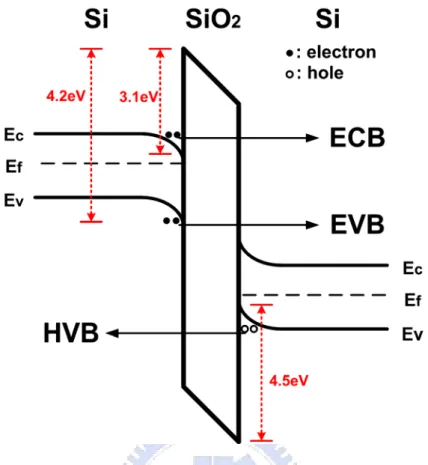
microelectronic applications. Since the structure consisted of metal, oxide, and semiconductor, the leakage mechanism inevitably existed. The leakage phenomenon had been investigated in the MOS structure early, and then three kinds of tunneling mechanisms [8]-[10] were observed to explain the leakage in the CMOS. There are ECB (electron tunneling from conduction band), EVB (electron tunneling from the valence band), and HVB (hole tunneling from valence band) in the leakage mechanism. Since the gate oxide was quite thick in the early CMOS processes, the gate leakage did not cause serious issue.
During 199x~200x, due to the demand of high driving current, high operating speed, and lower power consumption, the CMOS technology was scaled down toward shorter channel length, thinner gate-oxide thickness, and lower power-supply voltage. As a result, the gate leakage current can no longer be ignored, because it is larger than the order of nA). To account for this effect, the gate-direct-tunneling-current model had been proposed in BSIM4 model [11]-[13] and it was released on Mar. 24, 2000 [14]. The proposed model was given by
3 3 OX 2 2 OX b 3 b n g OX OX b b OX OX V 8 2m 1 (1 ) q J C(V , V , T , ) exp 8 h 3hq E , (2.2) and g OX b OX g OX OX b b bo b OX V V V 20 C(V , V , T , ) exp ( 1) (1 ) ( ) N T (2.3)
where VOX is effective gate voltage, TOX is the oxide thickness, EOX is VOX/TOX, α is
the fitting parameter depending on the tunneling process, bo is the Si/SiO2 barrier
height (3.1eV for electron and 4.5eV for hole), and b is the actual tunneling barrier
height (e,q., 3.1eV for ECB, 4.2eV for EVB, and 4.5eV for HVB). N represents the density of carriers in the inversion or accumulation layer of the injecting electrode. For ECB and EVB tunneling process in both the inversion and accumulation regimes, N is expressed by
ge th g FB OX inv t acc t OX inv t acc t V V V V N n v ln 1 exp( ) n v ln 1 exp T n v n v (2.4)
where ninv and nacc denote the swing parameters, Vth is the threshold voltage, VFB is
the flat-band voltage, vt is the thermal voltage, and Vge is the gate voltage minus the
gate-depletion voltage (Vg-Vpoly).
For EVB tunneling process, N can be described as
OX g OX EVB t OX EVB t V N n v ln 1 exp T n v (2.5)
where g is Eg/q and nEVB is the fitting parameter.
2.2 Gate Tunneling Mechanisms Described With Energy-Band
Diagram
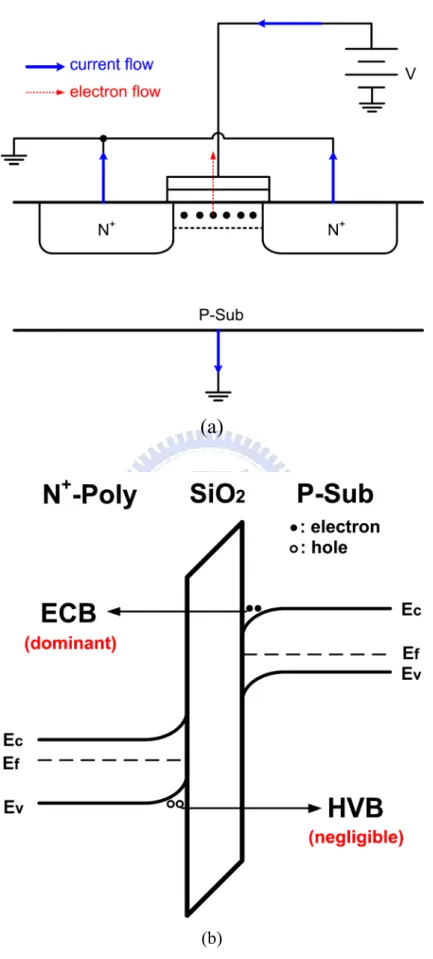
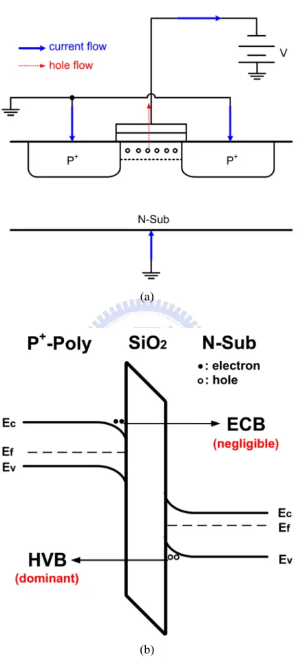
There are three kinds of tunneling mechanisms were observed to explain the leakage in CMOS technology and they are shown in Fig. 2.1. ECB is the electron tunneling from the conduction band across the oxide barrier. ECB basically needs 3.1eV before the electron has the probability to tunnel across the oxide barrier. EVB is the electron tunneling from the valence band across the oxide barrier. EVB basically needs 4.2eV before the electron has the probability to tunnel across the oxide barrier. HVB is the hole tunneling form the valence band across the oxide barrier. HVB basically needs 4.5eV before the hole has the probability to tunnel across the oxide barrier.
The main tunneling mechanism of NMOS is shown in Fig. 2.2. The N+-Poly gate
is connected to the high potential to create the inversion layer, so the electron energy band is reduced in the N+-Poly side. Corresponsively, the electron energy band is raised in the P-Sub side. Since the inversion layer is full of electron and is connected to N+ region, it has higher electron energy than that of P-Sub region. Consequently, the electron has higher probability to tunnel. Thus, ECB is the main tunneling mechanism of NMOS in inversion. On the other hand, the N+-Poly energy band has
larger hole energy. The HVB can be ignored because the hole is the minority carrier in the N+-Poly region.
The main tunneling mechanism in PMOS is shown in Fig. 2.3. The P+-Poly gate is connected to the low potential to create the inversion layer, so the P+-Poly electron energy band is raised. Corresponsively, the P-Sub electron energy band is reduced. Since the inversion layer is full of hole and is connected to P+ region, it has higher hole energy than that of the N-Sub region. Consequently, the hole has higher probability to tunnel. Therefore, HVB is the main tunneling mechanism of PMOS in inversion. On the other hand, the P+-Poly energy band has larger electron energy. The ECB can be ignored because the electron is minority carrier in the P+-Poly region.
2.3 Gate Direct Tunneling Current in BSIM4
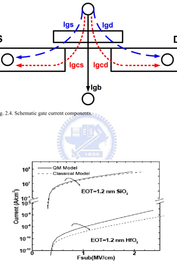
As the gate oxide thickness is scaled down to several nanometers or below, the gate leakage current becomes large due to direct tunneling of the carriers. The tunneling current happens between the gate terminal and silicon beneath the gate oxide. To reduce the tunneling current, different kinds of gate dielectrics have been studied to replace the traditional SiO2. To maintain good interface with the substrate,
multi-layer dielectric stacks have being proposed. The BSIM4 gate tunneling model has been demonstrated to work for multi-layer gate stacks as well. The gate direct tunneling components are shown in Fig. 2.4. The components include the tunneling current between the gate and substrate (Igb) and the current tunneling current between the gate and channel (Igc), which is partitioned between the source and drain terminals by Igc = Igcs + Igcd. The third component exists between the gate and source/drain diffusion regions (Igs and Igd).
2.3.1 Gate-to-Substrate Current (I
gb=I
gbacc+I
gbinv)
Igbacc, which is determined by ECB (electron tunneling from conduction band), is
significant in accumulation and is given by
gbacc eff eff oxRatio gb aux
oxacc oxacc
I W L A T V V
exp B TOXE(AIGBACC BIGBACC V ) 1 CIGBACC V
ToxRatio in (2.6) is expressed by NTOX oxRatio 2 TOXREF 1 T TOXE TOXE . (2.7) Vaux in (2.6) is given by gb fbzb aux t t V V
V NIGBACC v log[1 exp( )]
NIGBACC v
. (2.8)
Igbinv, which is determined by EVB (electron tunneling from valence band), is
significant in inversion and is given by
gbinv eff eff oxRatio gb aux
oxdepinv oxdepinv
I W L A T V V
exp B TOXE(AIGBINV BIGBINV V ) 1 CIGBINV V
. (2.9) ToxRatio in (2.9) is expressed by NTOX oxRatio 2 TOXREF 1 T TOXE TOXE . (2.10) Vaux in (2.9) is given by oxdepinv aux t t V EIGBINV
V NIGBINV v log 1 exp( )
NIGBINV v . (2.11)
2.3.2 Gate-to-Channel Current (I
gc0) and Gate-to-Source/Drain (I
gsand I
gd)
Igc0, which is determined by ECB (electron tunneling from conduction band) for
NMOS and HVB (hole tunneling from valence band) for PMOS at Vds=0, is
gc0 eff eff oxRatio gse aux
oxdepinv oxdepinv
I W L A T V V
exp B TOXE(AIGC BIGC V ) 1 CIGC V
. (2.12) ToxRatio in (2.12) is expressed by NTOX oxRatio 2 TOXREF 1 T TOXE TOXE . (2.13) Vaux in (2.12) is given by gse aux t t V VTH
V NIGC v log 1 exp( )
NIGC v . (2.14)
Igs represents the gate tunneling current between the gate and the source diffusion
region, while Igd represents the gate tunneling current between the gate and drain
diffusion region. Igs and Igd are determined by ECB for NMOS and HVB for PMOS,
respectively. Igs is expressed as
gs eff oxRatioEdge gs gs'
gs' gs'
I W DLCIG A T V V
exp B TOXE POXEDGE (AIGS BIGS V )(1 CIGS V )
. (2.15) ToxRationEdge is given by NTOX oxRatioEdge 2 TOXREF 1 T ( )
TOXE POXEDGE (TOXE POXEDGE)
. (2.16) Vgs’ is given by
2 4 gs' gs fbsd V V V 1.0e . (2.17) Vfbsd’ is given byB fbsd k T NGATE V log( ) VFBSDOEF q NSD . (2.18) Igd is expressed as gd eff oxRatioEdge gd gd ' gd ' gd' I W DLCIGD A T V V
exp B TOXE POXEDGE (AIGD BIGD V )(1 CIGD V )
. (2.19) Vgs’ is given by
2 4 gd ' gd fbsd V V V 1.0e . (2.20)2.3.3 Partition of I
gcConsidering the drain bias effect, Igc is split into two components, Igcs and Igcd,
namely, Igc=Igcs+Igcd. Igcs is given by
4 dseff
gcs gc0 2 2 4
dseff
PIGCD V exp( PIGCD) 1 1.0e
I I PIGCD V 2.0e . (2.21) PIGCD is expressed as dseff 2 gsteff gsteff V B TOXE PIGCD (1 ) V 2 V . (2.22) Igcd is given by 4 dseff gcd gc0 2 2 4 dseff
1 (PIGCD V 1) exp( PIGCD) 1.0e
I I PIGCD V 2.0e (2.23)
2.4 Gate Leakage Improvement with High-K Gate Dielectric
The drain current of MOS transistors is given by
2 ox GS th DS DS 1 W I C 2(V V )V V 2 L . (2.24)
In order to have high driving current, the oxide thickness is reduced to achieve larger Cox. The larger Cox not only increases the driving current but also increases the
operating speed. However, the interface will exist direct tunneling when the oxide thickness is scaled down to several nanometers or below. The situation becomes worse as the oxide thickness becomes thinner. In order to avoid the large gate leakage current, different kinds of gate dielectrics have been studied to replace the traditional SiO2. In other words, using other dielectrics can increase the oxide thickness without
decreasing the driving current. The capacitance in the dielectric layer is
0 d k C T . (2.25)
Using high-k dielectrics can increase the capacitance and maintain high driving current even if the thickness is thicker than that of SiO2. To maintain good interface
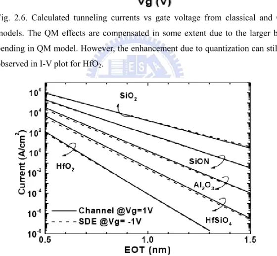
with substrate, multi-layer stacked dielectric layers had been proposed. Experiment results indicate that the leakage current was significantly be improved by using high-K dielectric [15] [16] and the gate leakage improvement form different kinds of gate dielectrics are shown in Fig. 2.5-Fig. 2.8.
Although the gate leakage current can be reduced by using high-k dielectric layers, high-k dielectric layers are available for all nanoscale CMOS processes.
(a)
(b)
Fig. 2.2. The tunneling mechanisms of NMOS in inversion (a) NMOS cross-sectional view in inversion (b) energy barrier figure.
(a)
(b)
Fig. 2.3. The tunneling mechanisms of PMOS in inversion: (a) PMOS cross-sectional view in inversion (b) Energy barrier figure.
Fig. 2.4. Schematic gate current components.
Fig. 2.5. Calculated dependence of tunneling current on substrate electric field for SiO2 and HfO2 by classical and quantum mechanical (QM) models. The quantization
Fig. 2.6. Calculated tunneling currents vs gate voltage from classical and QM models. The QM effects are compensated in some extent due to the larger band bending in QM model. However, the enhancement due to quantization can still be observed in I-V plot for HfO2.
Fig. 2.7. Simulated electron tunneling current of N-MOSFET vs EOT for various gate dielectrics. The substrate doping is 1018cm-3 and flat band voltage is thus -1.0V. For HfSiO4, K=13 and m=0.34m0 from an average of SiO2 and HfO2 values
are assumed. Al2O3 mole fraction is 30% for HfAlO and Si3N4 mole fraction 40
Fig. 2.8. Gate leakage as a function of Tinv for HfO2 for both Poly-Si and TiN gate dielectrodes. Also shown is SiON line for reference.
Chapter 3
Low-Leakage Power-Rail ESD Clamp Circuit
3.1 Leakage Issue in Traditional Power-Rail ESD Clamp Circuits
In traditional applications, the power-rail ESD clamp circuit was typically realized using the RC-based ESD-detection circuit and the main ESD clamping device. With the consideration for area efficiency, the capacitor was usually implemented with the MOS capacitor, because the MOS capacitor has the largest capacitance per unit area in generic CMOS processes. The conventional RC-based ESD-detection circuit shown in Fig. 3.1(a) is the most popular ESD-detection circuit in the power-rail ESD clamp circuit in submicron CMOS processes.
However, the gate leakage current issue becomes serious and can not be ignored in nanoscale CMOS processes. Because of the much thinner gate oxide in nanoscale CMOS processes, large gate leakage current has been observed when the MOS capacitor was utilized in the ESD-detection circuit. The leakage current of the MOS capacitor in the traditional ESD-detection circuit causes other leakage current paths, because the PMOS transistor (MP1, as shown in Fig. 3.1 (a)) in the ESD-detection
circuit can not be effectively turned off under normal circuit operating conditions, as shown in Fig. 3.1(b). Besides, the main ESD clamping device will be slightly turned on if the output voltage of the ESD-detection circuit is not at the required value. For example, the ESD clamping device realized by NMOS will leak current, because its gate voltage is not effectively biased to VSS. To avoid such a situation, some modified designs must be developed in nanoscale CMOS processes.
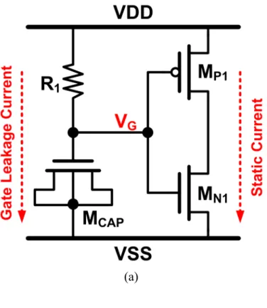
Some previous works had been reported to decrease the leakage current in the power-rail ESD clamp circuit [17]-[19]. These reported methods utilized circuit design techniques to reduce the leakage current. A power-rail ESD clamp circuit using stack structure and PMOS restorer to decrease circuit leakage current under normal circuit operating conditions had been proposed, as shown in Fig. 3.2 [17]. As shown in Fig. 3.3, another power-rail ESD clamp circuit using the PMOS and NMOS feedback to decrease the leakage current and improve the trigger ability is reported [18]. The PMOS MPFBK enhances the ability to turn off the ESD clamping device under normal circuit operating operations by further boost the drain voltage of MPINV1. The NMOS of MNFBK enhances the trigger ability under ESD transients
because the time interval in which the trigger current is provided is extended.
Another power-rail ESD clamp circuit using different paths to extend the delay time and reduce RC value to solve the fast power-on issue is shown in Fig. 3.4 [19]. Although the previous works can reduce the leakage current or reduce required RC value in the power-rail ESD clamp circuit, their ESD-detection circuits still utilize the traditional RC-based configuration. Since the power-supply voltage is across the MOS capacitor under normal circuit operating conditions, the gate leakage issue through the MOS capacitor still exists. In this thesis, a novel power-rail ESD clamp circuit is proposed to significantly reduce the leakage current within a compact layout area.
3.2 New Proposed Low-Leakage Power-Rail ESD Clamp Circuit
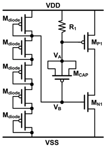
As discussed before, traditional power-rail ESD clamp circuits can not be used in nanoscale CMOS processes anymore because of the leakage current through the gate oxide. To solve this issue a new design is proposed in this thesis. The new proposed low-leakage ESD-detection circuit is shown in Fig. 3.5. The new proposed low-leakage ESD-detection circuit has simple structure and compact layout area so that it can be easily applied to the I/O cells.
The new proposed ESD-detection circuit can solve the leakage issue in the power-rail ESD clamp circuit by using only thin-oxide devices. The silicon-controlled-rectifier (SCR) can be used instead of the large NMOS device as the main ESD clamping device, because SCR had been proven to have the highest ESD robustness under the smallest device size [20]. In section 2.3, the equations indicate that leakage current through the MOS capacitor can be reduced by reducing the voltage across the MOS capacitor. In Fig. 3.5, the MOS capacitor is connected between terminal VA and VB. This is different from the traditional design. The reason
is to avoid the MOS capacitor which has a leakage path to ground. Diode-connected PMOS transistors are used to bias the node of VB to reduce the voltage across the
MOS capacitor. The static current through diode-connected PMOS transistors can be reduced by increasing their channel lengths. With enough diode-connected PMOS transistor stacked between VDD and VSS, the voltage across the MOS capacitor can be decreased to reduce the leakage current. PMOS capacitor is used in the new proposed ESD-detection circuit because the MOS capacitor is not connected to VSS
and it has less gate leakage current than NMOS capacitor. Under normal circuit operating conditions, the new proposed ESD-detection circuit will not generate a serious leakage current.
The RC-delay determines the time in which the trigger current is provided. The size of PMOS MP1 determines the amount of trigger current. Larger MP1 leas to larger
trigger current, which can turn on the ESD clamping device more quickly. However, larger MP1 introduces more leakage current under normal circuit operating conditions.
3.3 Simulations on Leakage Currents of NMOS and PMOS
Capacitors in Nanoscale CMOS Processes
As the gate oxide thickness is scaled down to several nanometers or below, the gate leakage issue is serious. In the BSIM4 model (Hspice Level 54), the gate-tunneling current model has been included. In this section, the simulated results on the gate leakage current in nanoscale CMOS processes are presented.
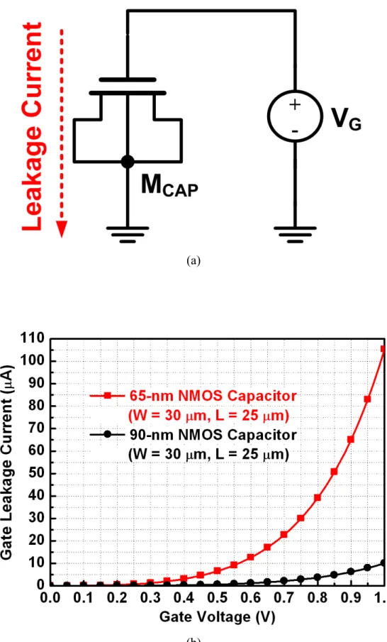
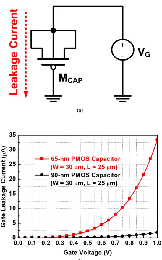
Fig. 3.6 (a) shows the simulation schematic of NMOS capacitor and Fig 3.6 (b) show the simulation results on the gate leakage currents of 65-nm and 90-nm thin-oxide NMOS capacitors under different gate voltages. Fig. 3.7 (a) shows the simulation schematic of PMOS capacitor and Fig 3.7 (b) show the simulation results on the gate leakage currents of 65-nm and 90-nm thin-oxide PMOS capacitors under different gate voltages. Fig. 3.8 and 3.9 show the simulated results on the gate leakage currents of 65-nm thin-oxide NMOS and PMOS capacitors at different temperatures and gate leakage current at VG = 1 under different temperatures are listed in Table 3.1.
The simulation schematic of MOS capacitor is the same as Fig 3.6(a) and Fig 3.7 (b). According to the simulation results, the gate leakage current is increased when higher voltage is across the MOS capacitor. Simulation gate leakage currents of 65-nm and 90-nm MOS capacitors at different gate voltages are listed in Table 3.2. At 25 °C, the leakage current is about 105 A in a 65-nm thin-oxide NMOS capacitor with the size of 30 m × 25 m. At 25 °C, the leakage current is about 33.4A in a 65-nm thin-oxide PMOS capacitor with the size of 30 m × 25 m. At 25 °C, the leakage current is about 10 A in a 90-nm thin-oxide NMOS capacitor with the size of 30 m × 25 m. At 25 °C, the leakage current is about 1.87 A in a 90-nm thin-oxide PMOS capacitor with the size of 30m×25m. As expected, the gate leakage currents are lower in the 90-nm CMOS process than those in the 65-nm CMOS process. With the
evolution of CMOS processes, the gate leakage issue becomes worse due to the thinner gate oxide. The simulation results have shown that the traditional ESD-detection circuit is no longer feasible. The modified design to reduce the leakage current in the power-rail ESD circuit is required.
3.4 Simulation on Traditional and New Proposed ESD-detection
Circuit in Nanoscale CMOS process
In this section, the simulated results on the traditional and new proposed low-leakage ESD-detection circuits in a 65-nm CMOS process are presented. Fig. 3.10 shows the simulated result on leakage current of the traditional ESD-detection circuit (as shown in Fig. 3.1) under normal circuit operating conditions. The device dimensions in the traditional ESD-detection circuits are listed in Table 3.3. Due to the large leakage current of the MOS capacitor, the voltage at the inverter input node can not be charged to VDD and it is only ~0.6 V. Consequently, the NMOS and PMOS in the inverter are partially turned on have static current. At 25 °C, the total leakage from VDD is as high as 675 A, which is too high to be tolerated. As the simulated result suggesting, the serious gate leakage current of the MOS capacitor make the traditional ESD-detection circuit not suitable in nanoscale CMOS processes.
The previous work using the PMOS restorer is simplified and is shown in Fig. 3.11. The simulated result on leakage current of the ESD-detection circuit with the PMOS restorer under normal circuit operating conditions is shown in Fig. 3.12. The device dimensions used in Fig. 3.12 are listed in Table 3.4. The PMOS restorer is useful to enhance the ability to turn off the inverter PMOS (MP1). However, the
leakage current through the MOS capacitor still exists, which is 89 A at 25 °C. The leakage current is still too large.
Fig. 3.13 shows the simulated result on the leakage current of the new proposed ESD-detection circuit (as shown in Fig. 3.5.) under normal circuit operating conditions. Since the diode-connected PMOS string provides the bias voltage for the gate terminal of the MOS capacitor, the voltage across the MOS capacitor is decreased as compared with the MOS transistor in the traditional ESD-detection circuit. Therefore, the leakage current can be significantly reduced. Because of the reduced leakage current and the higher gate voltage of the MOS capacitor, the voltage of terminal VA can be charged to high enough voltage close to VDD to fully turn off
the inverter PMOS (MP1) to reduce the leakage current. At 25 °C, the total leakage
from VDD is only 215 A. As compared with the traditional ESD-detection circuits, the proposed ESD-detection circuit has much lower leakage current. The device dimensions used in the proposed ESD-detection circuit are listed in Table 3.5. Since RC-delay and the PMOS MP1 is initially turned-on, the new proposed ESD-detection
can provide trigger current to trigger on the ESD clamping device during ESD stresses. In the simulation of trigger current, a 100-Ω resistor is connected between the trigger node and ground to emulate the substrate resistance of substrate-triggered SCR. The simulated trigger current provided by the new proposed low-leakage
ESD-detection circuit under ESD-like transients is shown in Fig. 3.14. With the trigger current of ~40 mA, the ESD clamping device can be quickly turned on to provide ESD current path between VDD and VSS.
Table 3.1
MOS capacitor simulated gate leakage current at VG = 1 V under different
temperatures
Table 3.2
Leakage current of NMOS and PMOS capacitor in different CMOS processes.
Table 3.3
Table 3.4
Device dimensions of traditional ESD-detection with restorer.
Table 3.5
(a)
(b)
Fig. 3.1. Gate leakage issue in the traditional ESD-detection circuit: (a) Traditional ESD-detection circuit (b) Circuit logic under MOS capacitor gate leakage issue.
Fig. 3.2. Proposed power-rail ESD clamp circuit in reference [15].
Fig. 3.4. Proposed power-rail ESD clamp circuit in reference [17].
(a)
(b)
Fig. 3.6. 65nm and 90nm NMOS capacitor gate leakage current simulations: (a) NMOS capacitor (b) Gate leakage current of PMOS capacitor in different CMOS processes.
(a)
(b)
Fig. 3.7. 65nm and 90nm PMOS capacitor gate leakage current simulations: (a) PMOS capacitor (b) Gate leakage current of PMOS capacitor in different CMOS processes.
Fig. 3.8. 65nm NMOS capacitor gate leakage current simulations at different temperatures.
Fig. 3.9. 65nm PMOS capacitor gate leakage current simulations at different temperatures.
Fig. 3.10. Traditional ESD-detection circuit simulation result of leakage current under normal circuit operating conditions.
Fig. 3.12. Traditional ESD-detection circuit with restorer simulated result of leakage current under normal circuit operating conditions.
Fig. 3.13. New proposed low-leakage ESD-detection circuit simulated result of leakage current under normal circuit operating conditions.
Fig. 3.14. New proposed low-leakage ESD-detection circuit simulated result under ESD-like transient.
Chapter 4
Experiment Results
In this thesis, the test devices and circuits were fabricated in 65-nm and 90-nm CMOS processes to verify the new proposed low-leakage power-rail ESD clamp circuit in different nanoscale CMOS processes. Fig 4.1(a) and (b) shows the layout top view and the die photo of the test chip in a 65-nm CMOS process. Fig 4.2(a) and (b) shows the layout top view and the die photo of the test chip in a 90-nm CMOS process. Besides the proposed power-rail ESD clamp circuit, the two traditional power-rail ESD clamp circuits with the RC-based ESD-detection circuit and the PMOS restorer have also been fabricated for comparison. The two traditional ESD-detection circuits and the proposed ESD-detection circuit have been fabricated in the test chip. To investigate the leakage current of the MOS capacitor and the SCR device, the stand-alone MOS capacitors and SCR device have also been fabricated. In the three power-rail ESD clamp circuits, SCR is used as the main ESD clamping device. Because of SCR had been proven to have the highest ESD robustness under the smallest device size [20]. The experimental results contain three parts. The first part is the device characteristics. The second part is the leakage current of each power-rail ESD clamp circuit. The third part is the characteristics of each power-rail ESD clamp circuit under ESD stresses.
4.1. Devices Characteristics
In this section, the measured leakage currents of the fabricated MOS capacitor and SCR devices under different conditions are presented. The setup to measure the leakage current of the NMOS capacitor is the same as Fig. 3.6(a). Fig 4.3 shows the measured gate leakage current of the 65-nm thin-oxide NMOS capacitor at different temperatures. With the dimensions of 30 μm × 25 μm, the measured leakage current is 72 A under 1-V supply voltage at 25 °C. When the temperature is increased to 125 °C, the leakage current is increased to 85 A under the power-supply voltage of 1 V. The gate leakage current increases when the temperature is increased or the voltage across the NMOS is increased.
The setup to measure the leakage current of the PMOS capacitor is the same as Fig. 3.7(a). Fig 4.4 shows the measured gate leakage current of the 65-nm thin-oxide PMOS capacitor at different temperatures. With the dimensions of 30 μm × 25 μm, the measured leakage current is 19 A under 1-V supply voltage at 25 °C. When the temperature is increased to 125 °C, the leakage current is 22 A under the power-supply voltage of 1 V. The measured gate leakage current at VG = 1 under
different temperatures are listed in Table 4.1. Similarly, the gate leakage current increases when the temperature is increased or the voltage across the NMOS is increased.
The layout top view and cross-sectional view of the SCR are shown in Fig. 4.5(a) and (b), respectively. In the 65-nm CMOS process, the width of SCR is 60 μm. Fig 4.6(a) shows the measured leakage current of the SCR in a 65-nm CMOS process at different temperatures. During the measurement of leakage current, the anode of SCR is biased at 1 V with the cathode grounded. Fig 4.6(b) shows the DC I-V curves of the SCR. The holding voltage (~2 V) of SCR is larger than the supply voltage of 1 V, so it will not cause latchup trouble for 1-V IC applications.
In the 90-nm test chip, the the width of SCR is 60 μm. Fig 4.7(a) shows the measured leakage current of SCR in a 90-nm CMOS process under 1-V bias at different temperatures. Fig 4.7(b) shows the DC I-V curves of the SCR. Similarly, the holding voltage (~ 2 V) of SCR is larger than the supply voltage of 1.2 V, so it will not cause latchup trouble for 1.2-V IC applications, either. Since the leakage current of SCR is quite small and it is expected to sustain high ESD robustness under a small device size, SCR is used as the main ESD clamping device instead of the large NMOS transistor.
4.2.
Leakage Current of the Traditional and New Proposed
Power-Rail ESD Clamp Circuits
There are three kinds of power-rail ESD clamp circuits included in the test chips. Fig. 4.8 shows the traditional ESD clamp circuit. Fig. 4.9 shows the traditional power-rail ESD clamp circuit with the PMOS restorer. Fig. 4.10 shows the new proposed low-leakage ESD clamp circuit. The device dimensions in the ESD-detection circuits of these three power-rail ESD clamp circuits are listed in Table
3.3 to 3.5.
In the 65-nm CMOS process test chip, the leakage currents of the three power-rail ESD clamp circuits under different VDD voltages at 25 °C and 125 °C are compared in Fig. 4.11 and 4.12, respectively. Their leakage currents under 1-V VDD voltage are listed in Table 4.2. Compared with the leakage current of the stand-alone MOS capacitor, much higher leakage current is observed in the traditional design, which demonstrates that the leaky MOS capacitor causes other leakage current paths in the power-rail ESD clamp circuit. Although the leakage current is reduced by adding the restorer, it is still as high as 88 A under 1-V VDD and 25 °C. Under 1-V power-supply voltage, the new proposed power-rail ESD clamp circuit has the lowest leakage current, which is only 228 nA (3.14 A) at 25 °C (125 °C). The measured leakage currents among the three power-rail ESD clamp circuits at different temperatures are compared in Fig. 4.13 with 1-V power-supply voltage. The leakage current of the new proposed power-rail ESD clamp circuit is two orders lower than those of the two traditional power-rail ESD clamp circuits.
In the 90-nm CMOS process test chip, device dimensions are the same those used in the 65-nm test chip (as listed in Table 3.3 to 3.5). The measured leakage currents of the three power-rail ESD clamp circuits under different power-supply voltages at 25 °C and 125 °C are compared in Fig. 4.14 and 4.15, respectively. Their leakage currents under 1-V power-supply voltage are listed in Table 4.3. The new proposed design also has the lowest leakage current in the 90-nm CMOS process, which is only 87 nA (394 nA) at 25 °C (125 °C). The leakage currents among the three power-rail ESD clamp circuits at different temperatures are compared in Fig. 4.16 with 1-V power-supply voltage.
4.3 ESD Robustness of Traditional and New Proposed Power-Rail
ESD Clamp Circuits
In test chip fabricated in a 65-nm CMOS process, when a 5-V ESD-like voltage pulse with 2-ns rise time and 100-ns pulse width is applied to the VDD node of three power-rail ESD clamp circuits, the VDD voltage is rapidly clamped to around 2 V within 5 ns, as shown in Fig. 4.17. The measured turn-on efficiency have demonstrated that the internal circuits can be well protected by the new proposed power-rail ESD clamp circuit. The human-body-model (HBM) and machine-model
(MM) ESD robustness among these three power-rail ESD clamp circuits have been characterized and listed in Table 4.4. The new proposed design has the ESD level of over 8 kV in HBM and 750 V in MM, respectively. Besides much lower leakage current, the proposed power-rail ESD clamp circuit can achieve comparable ESD robustness as compared with the traditional power-rail ESD clamp circuits.
The turn-on efficiency has also been investigated for the test chip fabricated in a 90-nm CMOS process. When a 5-V ESD-like voltage pulse with 2-ns rise time and 100-ns pulse width is applied to the VDD node of three power-rail ESD clamp circuits, the VDD voltage is rapidly clamped to ~ 2.5 V within 5 ns, as shown in Fig. 4.18. Thus, the internal circuits can be also well protected by the new proposed power-rail ESD clamp circuit in a 90-nm CMOS process. With a holding of ~2.5 V, the SCR did not cause latchup trouble for 1-V IC applications. The HBM and MM ESD robustness among these three power-rail ESD clamp circuits fabricated in a 90-nm CMOS process are listed in Table 4.5. The new proposed design has the same ESD levels as those of the traditional power-rail ESD clamp circuits, which are over 8 kV in HBM and 500V in MM.
Table 4.1
MOS capacitor measured gate leakage current at VG = 1 V under different
temperatures
Table 4.2
Measured leakage currents of power-rail ESD clamp circuits in a 65-nm CMOS process
Table 4.3
Measured leakage currents of power-rail ESD Clamp circuits in a 90-nm CMOS process
Table 4.4
HBM and MM ESD robustness of power-rail ESD clamp circuits in a 65-nm CMOS process
Table 4.5
HBM and MM ESD robustness of power-rail ESD clamp circuits in a 90-nm CMOS process
(a)
(b)
Fig. 4.1 65-nm CMOS process test chip: (a) Layout top view of the test chip (b) Die photo of the test chip.
(a)
Fig. 4.2. 90-nm CMOS process test chip: (a) Layout top view of the test chip (b) Die photo of the test chip.
Fig. 4.3. Measured gate leakage current of the 65-nm NMOS capacitor at different temperatures.
Fig. 4.4. Measured gate leakage current of the 65-nm PMOS capacitor at different temperatures.
(a)
(b)
Fig. 4.5. Substrate-triggered SCR: (a) Layout top view and (b) Cross-sectional view of the substrate-triggered SCR.
(a)
(b)
Fig. 4.6. SCR characteristics in a 65-nm CMOS process: (a) SCR leakage current at different temperatures. (b) SCR DC I-V curves at different temperatures.
(a)
(b)
Fig. 4.7. SCR characteristics in a 90-nm CMOS process: (a) SCR leakage current at different temperatures. (b) SCR DC I-V curves at different temperatures.
Fig. 4.8. Traditional power-rail ESD clamp circuit. SCR is used as the ESD clamping device.
Fig. 4.9. Traditional power-rail ESD clamp circuit with the PMOS restorer. SCR is used as the ESD clamping device.
Fig. 4.10. New proposed power-rail ESD clamp circuit with SCR as the ESD clamping device.
Fig. 4.11. Comparison of the leakage currents among the traditional and the new proposed power-rail ESD clamp circuits in a 65-nm CMOS process with different VDD biases at room temperature of 25 °C.
Fig. 4.12. Comparison of the leakage currents among the traditional and the new proposed power-rail ESD clamp circuits in a 65-nm CMOS process with different VDD biases at high temperature of 125 °C.
Fig. 4.13. Comparison of the leakage currents at 1-V VDD among the traditional and the new proposed power-rail ESD clamp circuits in a 65-nm CMOS process at different temperatures.
Fig. 4.14. Comparison of the leakage currents among the traditional and the new proposed power-rail ESD clamp circuits in a 90-nm CMOS process with different VDD biases at room temperature of 25 °C.
Fig. 4.15. Comparison of the leakage currents among the traditional and the new proposed power-rail ESD clamp circuits in a 90-nm CMOS process with different VDD biases at high temperature of 125 °C.
Fig. 4.16. Comparison of the leakage currents at 1-V VDD among the traditional and the new proposed power-rail ESD clamp circuits in a 90-nm CMOS process at different temperatures.
Fig. 4.17. Comparison of the turn-on efficiency among the three power-rail ESD clamp circuits in a 65-nm CMOS process under the applied 5-V voltage pulse with a rise time of 2ns and a pulse width of 100ns.
Fig. 4.18. Comparison of the turn-on efficiency among the three power-rail ESD clamp circuits in a 90-nm CMOS process under the applied 5-V voltage pulse with a rise time of 2ns and a pulse width of 100ns.
Chapter 5
Discussions
The proposed ESD-detection circuit (shown in Fig. 3.5) uses diode-connected PMOS string to reduce the voltage across the MOS capacitor. With the proposed design, the leakage current through the MOS capacitor is reduced and the turned-off ability of the trigger PMOS (MP1) is enhanced under normal circuit operating
conditions. Thus, the proposed design does not suffer incorrect function and generates large leakage current. Besides, the diode-connected PMOS string is a good voltage divider. Even if there is a large variation in temperature, it still provides a regular voltage value, as shown in Fig. 6.1. The difference between VB at 25 °C and 125 °C is
only 8 mV. With the regular voltage of VB, the circuit function is not affected at high
temperature under normal circuit operating conditions. Since MP1 is at the
subthreshold region, slight increase of gate voltage causes significant subthreshold leakage current. The leakage current of the proposed ESD-detection circuit can be divided into three parts, the first part is through the diode-connected PMOS string; the second part is through the MOS capacitor, and the third part is through the trigger PMOS (MP1) and NMOS (MN1). The third part dominates the overall leakage current
under normal circuit operating conditions due to the subthreshold leakage current of large trigger PMOS (MP1) transistor.
In the test chip in a 90-nm CMOS process, the leakage currents of these three power-rail ESD clamp circuits become close when the temperature is increased. The test chip was fabricated in a low-leakage 90-nm CMOS process, so the thick-oxide MOS capacitor does not have obvious gate-leakage current, as described in section 3.1. The leakage currents of different power-rail ESD clamp circuits are dominated by the subthreshold leakage current of MOS transistors. The proposed design enhances the turned-off ability of the trigger PMOS (MP1), so the subthreshold current is
smaller than that in the traditional designs under low temperatures. These three power-rail ESD clamp circuits use the same size of trigger PMOS (MP1) and NMOS
(MN1), and the increase of subthreshold leakage current correlated closely with
temperature. Since the subthreshold leakage current of MOS transistor dominate the overall leakage current, the leakage currents of these three power-rail ESD clamp
circuits became close when temperature is increased.
In the test chip in a 65-nm CMOS process, the thin-oxide MOS capacitor has large gate-leakage current, so the traditional ESD-detection circuit can not work correctly and it generates large leakage current, as the measured results shown in section 4.x. Although adding the PMOS restorer can enhance the turn-off ability of the trigger PMOS (MP1) and reduce the leakage current, the leakage current through
the MOS capacitor is still too large. The overall leakage current in the proposed design is dominated by the subthreshold leakage current of MOS transistors, which is increased significantly as the temperature is increased, as shown in Fig. 6.2. Since the trigger MOS transistors in the traditional designs are already turned on under normal circuit operating conditions, the increase of leakage current is slighter than that of the proposed design as the temperature is increased.
Fig. 5.1. Voltage of VB under different temperatures.
Chapter 6
Conclusions and Future Works
6.1. Conclusions
There are several previous works addressing the influences of gate-tunneling current on nanoscale CMOS ICs. For the ICs implemented in nanoscale CMOS processes, the gate leakage issue needs to be taken into consideration due to the thin gate oxides. In this thesis, a new low-leakage power-rail ESD clamp circuit designed with the consideration of gate-leakage issue has been proposed and verified in 90-nm and 65-nm CMOS processes. In the proposed power-rail ESD clamp circuit, the leakage current is significantly reduced even though only thin-oxide devices are used.
Measured results have shown that the traditional designs have suffered such a serious leakage current. The leakage current under normal circuit operating conditions has been demonstrated to be significantly reduced in the proposed low-leakage power-rail ESD clamp circuit. Realized with only thin-oxide devices, the proposed power-rail ESD clamp circuit has much lower leakage current as compared with the traditional designs. Moreover, the ESD robustness is not deteriorated and the circuit area is not increased. In this thesis, the ESD clamping device in all power-rail ESD clamp circuits is the substrate-triggered SCR. Since the holding voltage of SCR is higher than the power-supply voltage, it can be used as the ESD clamping device without causing latchup issue.
6.2. Future Works
Although low leakage current and high ESD robustness have been achieved in the proposed power-rail ESD clamp circuit, there are still some drawbacks in the new proposed low-leakage power-rail ESD clamp circuit. Since the gate voltage of the MOS capacitor is biased by the diode-connected PMOS transistors, the ESD voltage is easily coupled to the gate terminal of the MOS capacitor during ESD stresses. Due to the capacitive coupling effect caused by the diode-connected PMOS transistors, the actual delay time provided by the RC timer is decreased than the expected value. As a result, the trigger ability during ESD stresses is degraded. Besides, using the
diode-connected PMOS transistors between VDD and VSS causes some static current flowing through them under normal circuit operating conditions. This static current is undesired and needs to be eliminated. In order to solve the problems in the proposed power-rail ESD clamp circuit, some techniques need to be developed in the near future.
![Fig. 3.3. Proposed power-rail ESD clamp circuit in reference [16].](https://thumb-ap.123doks.com/thumbv2/9libinfo/8409342.179750/41.892.135.796.589.946/fig-proposed-power-rail-esd-clamp-circuit-reference.webp)