國 立 交 通 大 學
電子工程學系 電子研究所
博 士 論 文
高介電係數閘極介電層在金氧半電晶體中
之電特性及其可靠度研究
A Study of Electrical Characteristics and Reliability
in CMOSFETs with High-κ Gate Dielectrics
研 究 生 : 陳世璋
指導教授 : 羅正忠 博士
簡昭欣 博士
高介電係數閘極介電層在金氧半電晶體中
之電特性及其可靠度研究
A Study of Electrical Characteristics and Reliability
in CMOSFETs with High-κ Gate Dielectrics
研 究 生:陳世璋
Student:Shih-Chang Chen
指導教授:羅正忠 博士
Advisor:Dr. Jen-Chung Lou
簡昭欣 博士
Dr. Chao-Hsin Chien
國 立 交 通 大 學
電子工程學系 電子研究所
博 士 論 文
A Dissertation
Submitted to Department of Electronics Engineering and
Institute of Electronics
College of Electrical and Computer Engineering
National Chiao Tung University
in Partial Fulfillment of the Requirements
for the Degree of
Doctor of Philosophy
In
Electronics Engineering
January, 2009
高介電係數閘極介電層在金氧半電晶體中
之電特性及其可靠度研究
研究生:陳世璋
指導教授:羅正忠 博士
簡昭欣 博士
國立交通大學
電子工程學系
電子研究所
摘要
隨著互補式金氧半電晶體(CMOSFETs)元件尺寸跟隨著摩爾定律(Moore’s Law)持續微縮,傳統的二氧化矽(SiO2)閘極介電層(Gate Dielectrics)將遭遇極大的直接穿
遂漏電流(Direct Tunneling Leakage Current)導致元件特性失效及可靠度衰退。而高 介電係數介電質(High-κ Dielectrics)具有較高的介電係數值,在保有較小的等效氧 化層厚度(Effective Oxide Thickness, EOT)情況下,可有效地降低因氧化層微縮至過 薄所帶來的巨大直接穿遂漏電流,並且同時保有良好的元件特性。因此高介電係 數介電層成為了取代二氧化矽作為下一新世代閘極介電層最有潛力的候選。然而 使用高介電係數介電層也將導致伴隨而來的幾個嚴重問題,包括了材料上的熱穩 定性(Thermal Stability)、費米能階鎖定效應(Fermi-Level Pinning Effect)、通道內載 子移動率的衰減(Mobility Degradation)、以及電荷被高介電係數介電層內之缺陷捕 捉/散逸之現象(Charge Trapping/De-trapping)……等等。由於介電質的熱穩定性、費 米能階鎖定效應、以及通道內載子移動率的衰減已分別可以藉由使用其它元素的 摻雜、金屬閘極的應用、以及利用應力效應來改善其影響,而電荷在高介電係數
本論文主要是探討高介電係數介電質的電特性及其可靠度研究,針對高介電係 數介電質所遭遇的問題,我們不僅在製程上尋求可以改善的適當方法,也有系統 地透過許多量測上的分析來瞭解電荷捕捉/散逸效應的相關物理機制。本論文一開 始的首章,我們將說明半導體製程上為何需要應用高介電係數介電層,以及在長 年相關研究之中所發現的幾個主要關鍵問題,並講解整個論文的組織架構。 在第二章中,我們利用製程技術針對高介電係數介電層的幾個關鍵問題來加以 改善元件特性。包括:(a)在與矽基板之界面特性研究中—我們成功地利用臭氧水 成長超薄氧化層(Ozone Oxide)來作為高介電係數介電質以及矽基板之間的中間介 電層(Interfacial Layer, IL),以有效地改善界面特性、抵抗大量的直接穿遂漏電流、 減少電荷捕捉/散逸效應,並且提升元件可靠度。(b) 在針對高介電係數介電層內 眾多的本體缺陷(Bulk Traps)—我們利用氟離子植入法(Fluorine Incorporation)有效 地修補高介電係數介電質的界面缺陷和本體內缺陷,降低電荷捕捉/散逸效應,並 提升元件之電特性及其可靠度。(c)在應用高介電係數介電質之後所造成的載子移 動率衰減—我們利用舒張性應力(Tensile Strain)在搭配高介電係數閘極介電層的 n 型金氧半電晶體(nMOSFETs)上進行元件特性的改善。我們有效地提升了 n 型金氧 半電晶體通道內的電子遷移率,並分析出應力效應的使用對元件電特性及其可靠 度之影響。此外,我們也從實驗中的結果發現電荷的捕捉效應無論是在 n 型通道 或P 型通道的高介電係數閘極介電層元件,都大大地主導其元件的可靠度特性。 在第三章中,我們仔細地研究高介電係數閘極介電層元件中之電荷捕捉效應 (Charge Trapping Effect)的物理機制及其對元件可靠度所帶來之影響。我們對 n 型 金氧半電晶體(nMOSFETs),在正電壓及嚴苛溫度條件下,研究元件可靠度之不穩 定性變化 (Positive Bias Temperature Instability, PBTI)。我們分析出在高介電係數介 電層中,電子被其本體缺陷的捕捉效應有著速度上及數量上的差別。在我們的量 測上,我們定義反應比較快的第一群組(0 ~ 1.78 sec)中所發生的捕捉效應為「快速
我們稱做「慢速捕捉」(Slow Trapping)。我們發現在 100 秒以內的 DC 量測中,快 速捕捉在數量上具有非常顯著的捕捉電荷量,並且對元件可靠度有著主導性的影 響。此外,我們也發現在Fowler Nordheim 穿遂現象的發生前後,電子由直接穿遂 過基底氧化層,進入高介電係數介電層而被其內的淺缺陷捕捉,轉變成電子先穿 遂到高介電係數介電層的導電帶,再被高介電係數介電層內的缺陷所捕捉。並且 整個電荷捕捉現象將完全由快速捕捉效應所主導。而經由實驗結果的分析以及相 關文獻的比對,我們也發現在高介電係數介電層HfO2中所反映出的這些快速捕捉
效應,主要是由HfO2中的Vo2+, Vo-, Vo2-等等的氧空乏缺陷(Oxygen Vacancies) 以
及晶體邊界缺陷 (grain boundary defects)所主導。
在第四章中,我們利用與第三章相同的元件及分析方式,有系統地分析研究回 復 電 壓(Recovery Voltage) 對 高 介 電 係 數 介 電 層 內 的 電 荷 的 散 逸 效 應 (Charge De-trapping Effect)所造成的影響。而電荷的散逸效應和捕捉效應同樣有著速度上及 數量上的差別,反應比較快的散逸效應我們定義為「快速散逸」,而相對較慢的 我們稱做「慢速散逸」。如同於電荷捕捉中的快速捕捉現象,快速散逸效應也在 整個電荷回復行為中具有著相當大的主導性。此外,我們發現整個電荷散逸效應 的物理機制,主要是由高介電係數介電層中被捕捉住的載子所可允許穿遂回矽基 板的能階所決定。 在第五章中,針對一般 DC 量測無法精準萃取到的快速暫態電荷捕捉/散逸效 應,我們也導入具有極短量測時間並可解析數奈秒(ns)下電荷行為之優勢的脈衝式 量測(Pulse IV Measurement),來正確完整的分析在高介電係數介電層中的電荷捕捉 /散逸效應。對幾個重要的物理參數,諸如:逼迫電壓,逼迫時間,回復電壓,以 及較嚴峻的操作溫度。我們分別有系統的進行完整的相關研究,並探討其背後的 物理意義。電荷的捕捉/散逸效應也經由溫度的相關性確定為電荷的穿遂效應所主 導。此外,我們也利用脈衝式量測模擬了高介電係數介電層元件在AC 電壓形式操
的電特性及可靠度仍有顯著的影響。 在第六章中,我們仔細地分析高介電係數閘極介電層元件在動態的連續操作電 壓下,電荷捕捉/散逸效應對其電特性及可靠度之影響。我們發現在回復電壓不足 的情況下,被捕捉在高介電係數介電層本體內部的電荷將會持續留存,並會累積 在下一次電荷捕捉效應之中。而透過一個足夠回復電壓的條件來分析,我們可以 知道整個電荷捕捉/散逸效應是具有回復性。進一步也證實在小電壓逼迫的條件 下,並無造成高介電係數介電層中任何額外的缺陷產生,只是重複電荷捕捉/散逸 的行為。因此,我們在動態電性逼迫之不穩定性測試中所看到元件的劣化,是由 於在高介電係數介電層本體中未能散逸而出的電荷,在重複的電荷捕捉/散逸效應 下造成了留存電荷的累積,而非在小電壓電性逼迫中產生新的缺陷。如此,我們 也映證了電荷的捕捉/散逸現象將對元件的連續操作造成顯著的影響。 在 第 七 章 中 , 我 們 對 具 有 高 介 電 係 數 閘 極 介 電 層 的 p 型金氧半電晶體 (pMOSFETs),在負電壓及嚴苛溫度條件下,研究元件可靠度之不穩定性變化 (Negative Bias Temperature Instability, NBTI)。在 NBTI 的研究中,我們除了分析電
洞在高介電係數介電層中的被捕捉特性,也藉由一個奇異的NBTI 現象(Anomalous
NBTI Behavior),額外發現電子在 NBTI 的可靠度衰退中也扮演一個不可忽視的角
色。因此,當我們在利用NBTI 可靠度考量元件的生命週期之時,我們必須慎重地 同時考量電子和電洞在 p 型高介電係數閘極電晶體中的捕捉現象,並以此修正整 個元件生命週期的預測。 在第八章中,我們總結了所有的研究成果,於高介電係數介電層的可靠度研究 中,我們在考量了電荷的快速暫態行為所帶來的影響,建立了一個具有合理解釋 的物理模型,並可有效地說明在高介電係數介電層中之電荷捕捉/散逸效應的物理 機制。最後,我們也根據這些年來研究高介電係數介電層的經驗,針對高介電係
A Study of Electrical Characteristics and Reliability in
CMOSFETs with High-
κ Gate Dielectrics
Student: Shih-Chang Chen Advisor: Dr. Jen-Chung Lou
Dr. Chao-Hsin Chien
Department of Electronics Engineering
& Institute of Electronics
National Chiao Tung University
Abstract
As the CMOS technology continues to scale down following the Moore’s Law, the shrinkage of gate dielectric thickness will suffer the intolerable direct-tunneling gate leakage-current which leads to degrade the device performance and reliability. High permittivity dielectrics (High-κ Dielectrics) have been proposed to be the potential candidates to solve the critical issues since their thicker films can be utilized to effectively reduce the great direct tunneling leakage current while it maintains EOT (Effective Oxide Thickness) value and the device performances. However, several critical problems such as thermal stability, Fermi-level pinning effect, channel mobility degradation, and charge trapping/de-trapping effects have been accompanied with the applications of high-κ gate dielectrics. The thermal stability, Fermi-level pinning effect, channel mobility degradation have been improved through the multi-element
the charge trapping/de-trapping effects are still the major difficulties which are waiting for the effective solutions in the progress of the high-κ gate dielectrics.
In the dissertation, we would mainly discuss the electrical characteristics and device reliability of high-κ gate dielectrics. For the derivative issues of high-κ gate dielectrics applications, we not only effectively enhance the device performance through appropriate fabrication technologies, but also systematically investigate the physical mechanisms of charge trapping/de-trapping effects through a variety of electrical characterizations. At the beginning, in the chapter 1, we will explain the necessary of high-κ gate dielectrics applied on semiconductor progress, and further point out several critical issues discovered during related investigations in recent years. Besides, we finally describe the organization of this dissertation.
In the early stages of this dissertation, we study the enhancements of device performance through the fabrication technologies. In the chapter 2, the ozone oxidation has been successful as an interfacial layer (IL) to apparently improve the interface between high-κ gate dielectrics and Si-substrate with fine interface properties, low direct tunneling leakage current, and less charge trapping effect. The fluorine incorporation has been confirmed to effectively reduce the interface states, high-κ bulk traps, and further suppress the charge trapping/de-trapping effects. Moreover, the device performance and related reliability are also successfully enhanced by fluorine incorporation. The tensile strain effect has been demonstrated to successfully enhance the device performance for nMOSFETs with high-κ gate stack. We have effectively enhanced the n-channel electron mobility and further investigated the influences of strain effect on device characterizations and related reliability. Besides, the charge trapping effect has been verified to dominate the reliability degradation in both
In the chapter 3, we have carefully studied the physical mechanism of charge trapping effect in high-κ gate dielectrics and its impacts on device reliability. In the reliability investigations of positive bias temperature instability (PBTI) on the nMOSFETs, we observed that the charge trapping phenomenon at high-κ bulk traps has the different characteristics with respect to responding time constant and quantity. In our measurements, we have defined the charge trapping occurred on the first stage (0 ~ 1.78 sec) as the “First Trapping”, and the second stage (1.78 ~ 100 sec) as the “Slow Trapping”. We have discovered that the fast trapping has the apparently significant impacts on device reliability with a great quantity of trapped charges during a 100 sec electrical stress in DC measurements. Moreover, we also found the distinct charge trapping behaviors before and after the occurrence of Fowler Nordheim tunneling (FN-tunneling). Before FN-tunneling, the injected charges form Si-substrate will tunnel through the IL and further be trapped at those shallow traps in the high-κ bulk. After FN-tunneling, the injected charges form Si-substrate still tunnel through the IL but drop on the conduction band of high-κ gate dielectrics. Afterward, these charges are captured from the conduction band of high-κ gate dielectrics by those shallow traps in high-κ bulk. From the experimental analysis and related literatures, we also have discovered that the oxygen vacancies (Vo2+, Vo-, Vo2-) and grain boundary defects are the main shallow traps which are responsible for the fast trapping in HfO2.
In the chapter 4, we have systematically investigated the influences of recovery voltage on charge de-trapping effect in high-κ gate dielectrics with the same devices and similar analytic methodologies in chapter 3. The charge de-trapping effect also shows the different responding time constant and quantity as well as charge trapping effect. The charge de-trapping with short time respondence is defined as “fast
(Recovery Time = 1.78 ~ 100 sec) is defined as “slow de-trapping” As the finding of the fast trapping in charge trapping phenomenon, the fast de-trapping is also significantly predominant in whole recovery behavior. Furthermore, we discover the physical mechanism of charge de-trapping effect is mainly determined by the trapped charges in high-κ bulk which can tunnel through the available energy levels back to Si-substrate.
In the chapter 5, a pulse IV measurement which can capture the real electrical characteristics within only several nano seconds (ns) is introduced to accurately realize the charge trapping/de-trapping effects in high-κ gate dielectrics since the fast transient charge trapping/de-trapping behaviors can not be actually presented in conventional DC measurements. We have systematically investigated the impacts of some significantly physical parameters such as stress voltage, stress time, recovery voltage, and crucial operation temperature on the complete phenomena and detailed mechanisms of charge trapping/de-trapping effects. Lower activation energy extracted form the temperature dependence demonstrates that the charge tunneling is the predominance for both charge trapping/de-trapping dynamics. Besides, the electrical characteristics of high-κ gate stack also have been analyzed under the AC stress conditions. We demonstrate that the charge trapping/de-trapping effects have apparent influences on device performance and related reliability under the AC operation.
In the chapter 6, we have carefully discussed the dynamic-PBTI degradation in nMOSFETs with high-κ gate stack in order to understand the impacts of charge trapping/de-trapping effects on the continuing device operation. We observe that the trapped charges which are not recoverable under the insufficient recovery voltage will be residual in high-κ bulk and further contribute to the significant PBTI degradation in next charge trapping sequence. The charge trapping/de-trapping phenomena are verified
smaller stress condition because the full recovery can be achieved with an appropriate recovery voltage. Therefore, we have realize the connection of residual charges with dynamic PBTI degradation, and further confirmed the apparent influences of charge trapping/de-trapping phenomena on the continuing device operation.
In the chapter 7, we discover a anomalous negative bias temperature instability (Anomalous NBTI) behavior in pMOSFETs with high-κ gate stack. This specific phenomenon is verified to be the contribution of electron trapping in high-κ bulk through a variety of electrical measurements including the threshold voltage shift, NBTI degradation, and charge pumping results. For the most important implication of anomalous NBTI discovery, the linear lifetime extraction is not able to accurately predict the lifetime at normal operation with high-κ gate stack once we consider both electron trapping and hole trapping in high-κ bulk traps.
In the chapter 8, we summarize all of the experimental results in the series of high-κ investigations. We build a reasonable physical model with the considerations of fast transient behaviors to appropriately explain the charge trapping/de-trapping effects in high-κ gate dielectrics. Finally, we also give some suggestions which are considered to be helpful to the realization and promotion of high-κ gate dielectrics applied on the CMOS technology.
謝誌
當博士畢業發表順利通過之際,內心所蘊含的百感交集已非點滴筆墨能足以 形容。是以,完成了一個當初為自己立下的里程碑,得到了不是結束一切的感覺, 反倒是有種替自己的人生打開了另一扇嶄新大門一般。帶著自己辛勤耕耘的收 穫,有著充滿了堅定的自信,很高興自己在完成博士學位的時候,能夠驕傲並榮 耀地懷帶著這樣的心情。 我的博士論文能夠順利完成,首先要感謝的是我最敬重的兩位指導教授—羅 正忠博士,以及簡昭欣博士。感謝兩位師長多年來在研究上給予悉心的指導以及 諄諄的教誨,其認真嚴謹的治學態度使我瞭解到了研究的真正精神,也讓我有機 會在研究的過程中,學習透過獨立思考使自己從青澀之中逐漸蛻變成長。而在日 常生活之中,他們也不時以其自身的經驗來與我分享待人處事的圓融與智慧。所 以,兩位師長不論在研究上和生活上都是我一生學習的典範。 再來我要特別感謝交大電子所的前期學長,現任於台積電的—吳偉豪博士。 感謝他在我博士研究過程中無私地分享許多寶貴的經驗,並交流諸多專業上的討 論與協助,使我得以深刻地體會身為一個博士所該具有的氣度與深度。更感謝偉 豪時時與我分享生活上的點滴智慧,在我身處研究過程低點之際,不斷真誠地鼓 舞我,引導我堅定意志突破難關。博士學位能順利完成,真的非常感謝偉豪的支 持及陪伴。 然後我也要感謝同為交大電子所的前期學長—陳永裕博士以及盧文泰博士。 感謝他們在我博士研究前期給予我許多實驗及量測技術上的指導及協助,使我得 以順利完成許多關鍵性的研究。此外,我要感謝台積電處長—Anthony S. Oates 博 士,謝謝他給與我機會能夠進入台積電開拓視野,這使我在研究討論以及解決問 題的思維上有了更進一步的成長,也讓我得以體驗許多工作上難得的學習與歷開拓許多。感謝Agilent Technology—林晉康先生,以及 Keithley Instruments—江培 仲先生。謝謝他們在硬體資源及量測技術上的大力協助,使我得以心無旁騖地專 心在研究中的關鍵量測上,讓我的研究成果能從一片片的矽晶片進而轉化成具有 參考性的物理意義。感謝交大半導體中心、國家奈米元件實驗室、以及交大電子 計測實驗室,感謝它們提供豐富的實驗及量測資源,讓我得以順利地進行研究上 的實作與分析。 感謝交大電子系所的—彭作煌先生,謝謝他與我分享許多待人接物的寶貴智 慧,並帶領我翻山越嶺接觸大自然,讓我在身處繁重的研究事務之中,亦能獲得 一個健康的平衡。感謝交大人才培訓中心的同仁—文鈴、欣梅、秋雲,謝謝妳們 在我課程資源上以及研究過程中的熱心協助,於生活之中也一起共享許多快樂的 點滴。 感謝研究所時期的同窗好友—軍宏、鳴汶、泰瑞、哲緯、峻丞,謝謝你們在 我研究所時期一路不斷地互相打氣陪伴。無論是在路邊攤小炒歡飲的痛快,亦或 是一起品嚐咖啡、茶、葡萄酒的感性,還有同在羽球場上的暢汗淋漓,所有的快 意與歡笑都是這一路上最棒的繽紛色彩!感謝在研究過程之中一同努力奮鬥的伙 伴們—韶華、彥銘、交力諭以及其它的同學、學弟妹,謝謝你們一起在研究上的 辛勞與共,點滴酸甜盡收藏於心。 感謝大學摯友—世青、鳴旭、佑松、翰陽、文敏、仁杰、育正,謝謝你們一 起陪伴我走過許多快樂及辛苦的時刻,真正的情誼是經得起時間的考驗,我見證 到了這些珍貴,沒有什麼可以比得上你們真摯的情意!當然我可沒忘了一直都默 契十足的Friends Four—宗緯(怡甄)、宗憲、欣倚,謝謝你(妳)們一起和我分享生活 中珍貴的點點滴滴—從有人戀愛的快樂、失戀的痛苦、到有人結婚的欣喜、生子 的滿足,我們總是彼此在失意時最安慰的依靠,在快樂時最棒的分享。我們也總 有著天馬行空令人發噱的突發奇想,有著最冷的笑話,還有著最不計形象的開懷
此外,在這邊我要特別感謝幾位在我生命中格外重要的摯友—友正、大偉(麗 惠)、彬舫(佳瑾)、德慶、以及建羽,謝謝你(妳)們在我這個旅程上不論如何的高低 起伏,始終如一的支持鼓勵著我,讓我得以堅定地完成這個重要的里程碑。說謝 謝已不足以言喻內心的一切感動,就讓我將這份真摯可貴的情誼收藏在我們每一 次欣喜見面時的擊掌與擁抱吧! 感謝欣怡,每一口熱茶的芬芳是溫暖;每一份料理的美味是窩心。妳的分享 與陪伴是我生命中美好的喜悅,於平凡之中我們一起擁有許多珍貴的滿足與感 動。是生活,是愛;是優雅,是美。由衷感謝有妳的美好,我生命中的美麗。當 我們擁抱彼此,就是最無與倫比的快樂與幸福! 最後,我要由衷地感謝我的家人—我的父親、母親、還有我最親愛的小妹。 謝謝你(妳)們這麼多年來一直堅定地支持著我,讓我無後顧之憂完成我的博士學 位。親愛的家人,你們都是我的最重要的力量,是我在生命中永遠會一直守護的 愛,也希望我一直是你們最棒的驕傲與榮耀! 感謝諸多珍貴的人事物,讓我得以在生命之中焠煉成長,進而順利地完成了 這個里程碑。僅以此博士論文,獻給所有親愛我以及我深愛的人。 世璋 九十八年 一月
Contents
Abstract ( Chinese ) ... i
Abstract ( English )... v
Acknowledgement ... x
Contents... xiii
Table Captions ... xviii
Figure Captions ... xix
Chapter 1 Introduction
1.1 Motivation of Using High-κ Gate Dielectrics... 11.2 Critical Issues of High- k Gate Dielectrics ... 2
1.3 Dissertation Organization... 6
References ... 8
Chapter 2
The Enhancements of Device Performance for High-κ
Gate Dielectrics with Fabrication Technologies
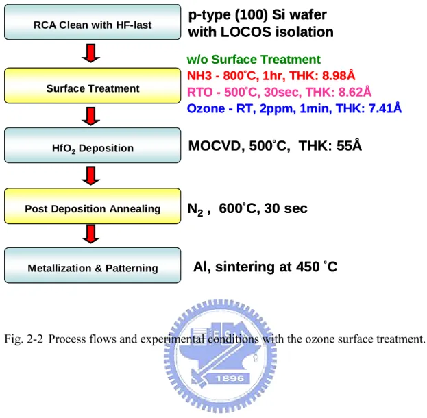
2.1 General Background ... 242.2 Improvements of Ozone Surface Treatment on the Electrical Characteristics and Reliability in HfO2 Gate Stacks... 24
2.2.1 Motivation ...24
2.2.2 Experimental Procedures...25
2.2.3 Results and Discussions...26
2.2.4 Summary ...28
2.3 The Effect of Fluorine Incorporation on pMOSFETs with HfO2/SiON Gate Stack ... 29
2.3.1 Motivation ...29
2.3.2 Experimental Procedures...30
2.3.3 Results and Discussions...31
2.3.3.1 Electrical Characteristics……….. 31
2.3.3.2 NBTI Investigations………... 32
2.3.4 Summary ...33
2.4 The Enhancements of Device Performance Using SiN Capping Layer on nMOSFETs with HfO2/SiON Gate Stack ... 34
2.4.1 Motivation ...34
2.4.2 Experimental Procedures...35
2.4.3 Results and Discussions...36
2.4.3.1 Electrical Characteristics……….. 36
2.4.3.2 PBTI Degradation and Traps Properties………. 37
2.4.4 Summary ...40
References ... 41
Chapter 3 Charge Trapping Behavior in High-κ Gate Dielectrics
3.1 Introduction ... 863.2 Experimental Procedures ... 87
3.3 Results and Discussions... 87
High-κ Gate Dielectrics ...89
3.4 Summary ... 93
References ... 95
Chapter 4 Charge De-trapping Behavior in High-κ Gate Dielectrics
4.1 Introduction ... 1174.2 Experimental Procedures ... 118
4.3 Results and Discussions... 119
4.3.1 Modeling of Charge De-trapping Behavior ... 119
4.3.2 The Influences of Stress Voltage on Charge De-trapping Behaviors in High-κ Gate Dielectrics...120
4.3.3 The Influences of Recovery Voltage on Charge De-trapping Behaviors in High-κ Gate Dielectrics...122
4.4 Summary ... 124
References ... 126
Chapter 5 Fast Transient Charge Trapping/De-trapping in High-κ
Gate Dielectrics
5.1 Introduction ... 1475.2 Experimental Procedures ... 148
5.3 Results and Discussions... 149
5.3.1 The Impacts of Fast Transient Charge Trapping/De-trapping in High-κ Gate Dielectrics and The Necessary of Pulse IV Measurements ...149
Dielectrics ...153
5.4 Summary ... 154
References ... 156
Chapter 6 Dynamic Positive Bias Temperature Instability Behavior
in nMOSFETs with HfO
2/SiO
2Gate Stack
6.1 Introduction ... 1856.2 Experimental Procedures ... 186
6.3 Results and Discussions... 187
6.3.1 Dynamic PBTI in DC Measurements ...187
6.3.2 Dynamic PBTI in Pulse Measurements ...188
6.4 Summary ... 190
References ... 192
Chapter 7 Anomalous Negative Bias Temperature Instability
Behavior in pMOSFETs with HfO
2/SiON Gate Stack
7.1 Introduction ... 2067.2 Experimental Procedures ... 207
7.3 Results and Discussions... 208
7.3.1 Anomalous NBTI Behaviors...208
7.3.2 Charge Pumping Methodology ...210
7.3.3 AC Characteristics ... 211
References ... 213
Chapter 8 Conclusions and Future Works
8.1 Summary of Findings and Contributions... 2318.2 Suggestions for Future Works... 234
Vita………237
Table Captions
Chapter 1 Introduction
Table 1-1 EOT scaling in the International Technology Roadmap for Semiconductor,
2007 edition………..………..……17
Chapter 3 Charge Trapping Behavior in High-κ Gate Dielectrics
Table 3-1 Fitting parameters in modeling of charge trapping in nMOSFETs with
Poly-Si/HfO2/SiON gate………...………..…..101
Table 3-2 Modeling fitting of charge trapping before and after FN-tunneling……..114
Chapter 4 Charge De-trapping Behavior in High-κ Gate Dielectrics
Table 4-1 Modeling fitting of charge de-trapping under all stress voltages………..139Figure Captions
Chapter 1 Introduction
Fig. 1-1 HRTEM pictures of the HfO2 with various high temperature annealing (a)
as-deposited state, 400 °C, (b) 800 °C annealing, (c) 900 °C annealing, (d) 1000 °C annealing, respectively…………...………...……..……18
Fig. 1-2 The Fermi-level pinning effect in high-κ gate dielectrics revealed in C-V characteristics (a) SiON (b) HfAlOx (c) HfSiOx………..……….……19
Fig. 1-3 Significant mobility degradation in the devices with poly-Si/high-κ gate dielectrics. The mobility can be improved with mid-gap metal gate electrode by screening the remote phonons scattering…..………20
Fig. 1-4 Interface dipole is considered as the primary origin of significant mobility degradation………...………...……..……21
Fig. 1-5 The strain engineering for High-k FETs (a) nMOSFETs (b) pMOSFETs………..……..……22
Fig. 1-6 The charge trapping/de-trapping phenomena in (a) Dynamic-PBTI, nMOSFETs (b) Dynamic-NBTI, pMOSFETs. ………...………..……23
Fig. 2-1 Key issues of high-κ gate dielectrics applied on CMOS technology………47 Fig. 2-2 Process flows and experimental conditions with the ozone surface
treatment………48
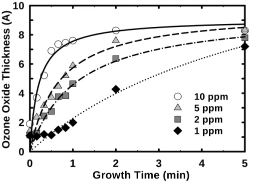
Fig. 2-3 Growth curves of ozone-mediated oxides plotted as a function of the concentration of ozone in water………49
Fig. 2-4 Comparison of the etching rates at HF:H2O = 1:500 of the ozone-mediated
oxide to that of the chemical oxide formed by RCA cleaning without HF-last………...………50
Fig. 2-5 HRTEM image of the ozone-treated HfO2 after PDA at 600 °C………...…51
Fig. 2-6 (a) Ozone-treated HfO2 w/o PDA (b) Ozone-treated HfO2 with PDA.
Ozone-treated HfO2 with an appropriate PDA exhibit the improved interface,
and the less hysteresis even after a severe electrical stress………...…52
Fig. 2-7 Leakage current density of HfO2 gate stacks with respect to the various
surface treatment processes………...………53
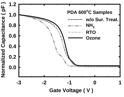
Fig. 2-8 C-V characteristics of HfO2 stacked gate dielectrics with respect to various
surface treatment processes………...………54
Fig. 2-9 Hysteresis curves obtained with respect to the various surface treatment processes………...……….…55
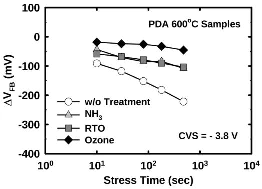
Fig. 2-11 Charge trapping effects plotted with respect to the various surface treatment processes………...……….……57
Fig. 2-12 Investigations of reliability obtained in TDDB measurements with respect to the various surface treatment processes……….…58
Fig. 2-13 Process flow of fluorine incorporation………..……59
Fig. 2-14 SIMS profile of fluorine incorporation into Hf-based high-κ gate dielectrics…..………..………..……….…60
Fig. 2-15 Effect of fluorine incorporation was shown on C-V characteristics. A positive C-V shift was according to the diffusion of fluorine atom into
HfO2..………..……….….…….……61
Fig. 2-16 The Id-Vg characteristics showed the influences of fluorine incorporation.
The mechanism of positive Vt shift was similar to the C-V behavior due to
fluorine diffusion into HfO2. The enhanced Gm revealed the improvement at
interface of gate dielectric/Si-substrate because of F-Si bonding by fluorine incorporation……….……….……62
Fig. 2-17 The Id-Vd characteristics showed the enhancement of Fluorine incorporation
on device driving current…………..……….……63
Fig. 2-18 The dependence of channel length on (a) threshold voltage, Vt (b) maximum
demonstrated by charge pumping current………...………...65
Fig. 2-20 The interface degradation in various fluorine dose conditions was investigated after electrical stress……….………….……66
Fig. 2-21 Two-frequency charge pumping method revealed the characteristics of interface state and high-κ bulk traps………...….……67 Fig. 2-22 The influence of temperature effect on interface degradation was studied
through the NBTI process………...……….……68
Fig. 2-23 The NBTI degradation was investigated with respect to Fluorine dose conditions. The fluorine-incorporated samples showed a robust ability for reliability characteristics even at 125oC…..………….……….……69
Fig. 2-24 The behavior of total trap generation during NBTI degradation.…..………70
Fig. 2-25 The whole NBTI degradation was dominated by high-κ bulk degradation rather than the interface degradation…..………..……….……71
Fig. 2-26 Carrier mobility was extracted by Split-CV method. The enhanced mobility may be according to the reduction of remote phonon scattering because of fluorine incorporation repaired high-k bulk traps…..….………..…72
Fig. 2-27 Mechanism of strain effect influences on the enhancements of channel mobility…..………..……….……73
Fig. 2-29 (a) C-V characteristics were identical with various CESLs strain conditions. (b) Extracted EOT form C-V characteristics were between 2.2~2.4 nm.….75
Fig. 2-30 The enhancements of CESLs strain effects exhibited in (a) Id-Vg
characteristics (b) Gm-Vg characteristics…..……….……76
Fig. 2-31 The CESLs strain effect were demonstrated in the enhanced driving current…..……….……….……77
Fig. 2-32 The channel length dependences on Gm.MAX. The enhancements of strain
effect were apparently observed in short channel length…..………….……78
Fig. 2-33 Interface properties at SiON/Si-substrate were investigated through charge pumping method. A reduces of donor-like traps and interface states were found because a hydrogen passivation was conducted during SiN deposition by PECVD…..………..………….……79
Fig. 2-34 The PBTI degradation was investigated with respect to CESLs strain conditions. The experimental results were fine fitting with charge trapping model……….…..……….…….……80
Fig. 2-35 The dependences of stress voltage were also investigated in PBTI degradation…..……….……….……81
Fig. 2-36 Frenkel-Poole emission fitting was modeled for samples (a) w/o SiN capping. (b) 300nm SiN capping. The trap energy level with respect to conduction band of HfO2 was extracted as 0.92eV for w/o SiN capping and 0.93eV for
Fig. 2-37 Fowler-Nordheim tunneling fitting was modeled for samples w/o SiN capping and with 300nm SiN capping. The nearly identical slopes of FN-tunneling fitting indicated that CESLs strain effect did not change the trap energy levels and charge trapping behaviors in HfO2…..………..83
Fig. 2-38 Flicker noise results were investigated in samples w/o SiN and with 300nm SiN. The elevated γ value extracted from flicker noise signal indicated the increase of trap density after PBTI degradation…..………..84
Fig. 2-39 The effective trap density was transformed from flicker noise signal. The experimental results implied that samples with SiN capping had a severe charge trapping in high-κ bulk, and it led to more significant PBTI degradation…..……….……….……85
Chapter 3 Charge Trapping Behavior in High-κ Gate Dielectrics
Fig. 3-1 Impacts of charge trapping on (a) Threshold voltage instability and (b)
Transconductance, Gm…..……….……99
Fig. 3-2 The PBTI degradation under various stress voltages as a function of stress time…..……….………...100
Fig. 3-3 Modeling of charge trapping in nMOSFETs with Poly-Si/HfO2/SiON gate
stack. (a) Maximum of trapping charges, ΔVMAX (b) Trapping time constant,
stress voltage in high-κ gate dielectrics. The associated trap distribution is revealed by fitting parameter, γ…..………..………...…103 Fig. 3-5 A newly experimental results related to the traps generation under various
stress voltages in high-κ gate dielectrics. The associated trap distribution is revealed by fitting parameter, γ…..………..…..………….…104 Fig. 3-6 A definition of fast trapping (t = 0 ~ 1.78 sec) and slow trapping (t = 1.78 ~
100 sec) in our studies for the PBTI measurement with the conventional DC method…..……….………..……105
Fig. 3-7 Analysis of fast trapping, slow trapping, and total trapping under various stress voltages (a) Based SiO2 = 0.8 nm (b) Based SiO2 = 1.4 nm………..106
Fig. 3-8 Fast/total trapping ratio during whole PBTI degradation under various stress voltages (a) Based SiO2 = 0.8 nm (b) Based SiO2 = 1.4 nm. [A fast/total
trapping ratio is defined as (fast trapping)/(total trapping) × 100 % in our studies] …..……….……….…107
Fig. 3-9 Comparisons of all charge trapping behaviors. (a) Fast trapping and slow trapping (b) Fast/total trapping ratio…..……….……...108
Fig. 3-10 The predominant conduction mechanism in the regime of gate voltage….109
Fig. 3-11 Frenkel-Poole emission (F-P) Fitting in the regime of stress voltage (a) Stress Vg = 0.6 ~ 1.0V (b) Stress Vg = 1.0 ~ 1.6V (c) Stress Vg = 1.6 ~
Fig. 3-12 Fowler Nordheim tunneling (FN) Fitting in the regime of stress voltage (a) Stress Vg = 1.6 ~ 2.0V (b) Stress Vg = 2.0 ~ 2.6V…..………...…111
Fig. 3-13 Band diagram of charge trapping under various stress Vg conditions. (a)
Stress Vg = 1.2V (b) Stress Vg = 1.5V (c) Stress Vg = 1.8V…..…………..112
Fig. 3-14 Modeling of charge trapping at various stress time as a function of stress voltage. (a) Before FN-tunneling, stress Vg = 1.2 ~ 1.6V (b) After
FN-tunneling, stress Vg = 1.6 ~ 2.0V…..……….………113
Fig. 3-15 Distinct charge trapping behaviors in various time demarcation (short-time stress, up to 2 ms ) (a) Stress Vg = 1.2V (b) Stress Vg = 1.6…..…………..115
Fig. 3-16 Distinct charge trapping behaviors in various demarcation of stress time (long-time stress, up to 104 sec) (a) Threshold voltage shift in PBTI degradation (b) Fast trapping and slow trapping behaviors versus stress time…..……….………...116
Chapter 4 Charge De-trapping Behavior in High-κ Gate Dielectrics
Fig. 4-1 Linear relation between normalized saturation drain current degradation andthreshold voltage shift (ΔVt) under various stress voltages…..……...…131
Fig. 4-2 Successful modeling fitting of charge de-trapping in HfO2/SiON gate stack
Fig. 4-4 A definition of fast de-trapping (t = 0 ~ 1.78 sec) and slow de-trapping (t = 1.78 ~ 100 sec) in our studies for the PBTI measurement with the conventional DC method…..……….…..134
Fig. 4-5 Analysis of fast de-trapping, slow de-trapping, and total de-trapping under various stress voltages (a) Based SiO2 = 0.8 nm (b) Based SiO2 = 1.4
nm………135
Fig. 4-6 Charge de-trapping behaviors in both based SiO2 = 0.8 nm and 1.4 nm under
various stress voltages (a) Recovered Vt shift (related to recovered charges)
(b) Non-recovered Vt shift (related to non-recovered charges) …..………136
Fig. 4-7 Charge de-trapping behaviors in both based SiO2 = 0.8 nm and 1.4 nm under various stress voltages (a) Recovery (%) (b) Fast/total de-trapping ratio. A fast/total de-trapping ratio is defined as (fast de-trapping)/(total de-trapping) × 100 % in our studies] …..…………...………...……….…..137
Fig. 4-8 Analysis of fast de-trapping, slow de-trapping, and total de-trapping under various stress voltages (a) Based SiO2 = 0.8 nm (b) Based SiO2 = 1.4
nm…..………..138
Fig. 4-9 Analysis of fast de-trapping, slow de-trapping, and total de-trapping under various recovery voltages (a) Based SiO2 = 0.8 nm (b) Based SiO2 = 1.4
nm…..………...……….…..140
charges) …..………..…….…..141
Fig. 4-11 Recovery (%) in both based SiO2 = 0.8 nm and 1.4 nm under various
recovery voltages. [Recovery (%) is defined as (total de-trapping)/(total trapping) × 100 % in our studies] …..………...…...….…..142
Fig. 4-12 (a) Fast/total de-trapping ratio under various recovery voltages. (b) Fast/total trapping ratio under various stress voltages illustrated in Fig. 3-9(a). [Fast/total de-trapping ratio is defined as (fast de-trapping)/(total trapping) × 100 % in our studies] …..………..……..143
Fig. 4-13 Band diagram of charge de-trapping under various recovery Vr conditions. (a)
Recovery Vr = 0V (b) Recovery Vr = -0.5V (c) Recovery Vr =
-1.6V…..……….……….144
Fig. 4-14 A schematic illustration of available de-trapping shallow traps under
recovery condition of Vr = 0V…..……….…..145
Fig. 4-15 The comparisons of charge de-trapping between based SiO2 = 0.8 nm and
1.4 nm under various recovery voltages. [Charge de-trapping ratio is defined as (Charge de-trapping in IL = 1.4 nm)/(Charge de-trapping in IL = 0.8 nm) in our studies] …..……….………..146
Chapter 5 Fast Transient Charge Trapping/De-trapping in high-κ
Gate Dielectrics
Fig. 5-1 The charge trapping investigations analyzed in the nMOSFETs with SiO2
gate dielectrics through the comparisons of DC measurement and pulse measurement (a) Driving current characteristics (b) Id-Vg and Gm-Vg
characteristics. A trapping-free result revealed in the matching of DC and pulse curves…..……….………..160
Fig. 5-2 The charge trapping investigations analyzed in the nMOSFETs with high-κ gate dielectrics through the comparisons of DC measurement and pulse measurement (a) Driving current characteristics (b) Id-Vg and Gm-Vg
characteristics. An apparent charge trapping effect revealed in the separation of DC and pulse curves…..………..161
Fig. 5-3 The transient pulse-IV output waveform investigated under various applied gate voltages. The charge trapping becomes more significant with elevated stress voltages…..………..………..162
Fig. 5-4 The Id-Vg characteristics were represented by DC and pulse measurements.
The pulse measurements do a real-time monitor avoid the fast transient charge trapping effect…..……….…….………..163
Fig. 5-5 Charge de-trapping during the PBTI degradation with the DC and pulse measurements. The pulse measurements do a real-time monitor avoid the fast transient charge de-trapping effect…..………..164
Fig. 5-6 PBTI degradation observed through the pulse measurements and the DC measurements over several decades…..………..165
Fig. 5-7 Modeling fitting of charge trapping in HfO2/SiO2 gate stack under various
stress voltages. (a) Pulse measurement (b) DC measurement…...………..166
Fig. 5-8 Modeling fitting of charge trapping in HfO2/SiO2 gate stack with both pulse
and DC measurements under various stress voltages. Fitting parameter (a) Trapping time constant, τ0 (b) Related trapping distribution, γ…..…….…167
Fig. 5-9 The dependence of stress voltage on charge trapping in high-κ gate dielectrics as a function of Power Law behavior…..………….…………..168
Fig. 5-10 The impacts of stress voltage on recovered charge and non-recovered charge in high-κ gate dielectrics…..……….………..169 Fig. 5-11 The impacts of stress voltage on the recovery (%) under various recovery
voltages…..……….………...………..170
Fig. 5-12 The dependence of stress time on charge trapping in high-κ gate dielectrics as a function of Logarithmic behavior…..……….…………..171
Fig. 5-13 The impacts of stress time on (a) Recovered charge and (b) Non-Recovered charge in high-κ gate dielectrics…..………..…………..172 Fig. 5-14 The charge de-trapping behaviors revealed on the recovery (%) under various
stress time conditions…..………..…….………..173
Fig. 5-15 The impacts of recovery voltage on recovered charge and non-recovered charge in high-κ gate dielectrics…..………..…..174
Fig. 5-16 The charge de-trapping behaviors revealed on the recovery (%) under various recovery voltage conditions…..……….………..175
Fig. 5-17 The temperature dependence on charge trapping/de-trapping in high-κ gate dielectrics under various stress conditions (a) Charge trapping (b) Charge de-trapping…..……….………..…..176
Fig. 5-18 The impacts of temperature on the recovery (%) under various recovery voltages…..………...………….………..177
Fig. 5-19 The schematic input waveforms of DC mode and AC mode in the pulse measurements…..……….………...178
Fig. 5-20 The comparisons between DC and AC behaviors in the charge trapping/de-trapping under various stress voltages. (a) Trapped charges after stress (b) Non-Recovered charges after recovery…..………..179
Fig. 5-21 The impacts of DC and AC modes on recovery (%) under various stress voltages…..……….…………...………..180
Fig. 5-22 The charge trapping behavior expressed by the AC/DC ratio as a function of linear relation…..………..……….………..…181
Fig. 5-23 A schematic illustration of AC input waveform and related AC frequency…..……….………..………182
Fig. 5-25 The impacts of AC frequency on charge de-trapping behaviors represented by recovery (%). A de-trapping behavior was limited close to f = 1M Hz…..……….………..…184
Chapter 6 Dynamic Positive Bias Temperature Instability Behavior in
nMOSFETs with HfO
2/SiO
2Gate Stack
Fig. 6-1 The dynamic positive bias temperature instability (DPBTI) under various stress voltages (a) Threshold voltage shift during DPBTI degradation (b) Ratio of (fast trapping)/(total trapping) during DPBTI degradation…..…..195
Fig. 6-2 The dynamic positive bias temperature instability (DPBTI) under various recovery voltages (a) Threshold voltage shift during DPBTI degradation (b) Ratio of (fast de-trapping)/(total de-trapping) during DPBTI degradation…… ………...196 Fig. 6-3 The fast transient charge de-trapping during DPBTI degradation under
various recovery voltages…..……….………..197
Fig. 6-4 The temperature dependence on fast transient charge de-trapping during DPBTI degradation under various recovery voltages…..……….198
Fig. 6-5 The residual Vt shift (non-recovered Vt shift) as a function of stress time
during DPBTI degradation under various recovery voltages…..………...199
Fig. 6-7 The impacts of temperature on the residual Vt shift during DPBTI
degradation. The result of Vr = 0 is the comparison with Vr = -2.0…..…...201
Fig. 6-8 The impacts of temperature on the recovery (%) during DPBTI degradation under various recovery voltages…..……….202
Fig. 6-9 The schematic band diagrams related to the influences of the elevated temperature on the fast transient charge trapping/de-trapping during the DPBTI degradation. The trap-assisted conduction mechanisms become more active at higher temperature…..………...203
Fig. 6-10 The impacts of stress voltage (Vg) on the charge trapping/de-trapping
behaviors during DPBTI degradation under various recovery voltages. (a) Recovered Vt shift (b) Residual Vt shift…..……….……204
Fig. 6-11 The impacts of stress voltage on the recovery (%) during DPBTI degradation under various recovery voltages…..……….………205
Chapter 7 Anomalous Negative Bias Temperature Instability
Behavior in pMOSFETs with HfO2/SiON Gate Stack
Fig. 7-1 Sequences of negative bias temperature instability (NBTI) …..…………..216
Fig. 7-2 (a) The NBTI degradation under various stress conditions at 25 oC. (b) Anomalous NBTI degradation showed in Fig.7-1(a) …..………217
Fig. 7-4 Impact of temperature on threshold voltage shift during NBTI degradation…..……….………219
Fig. 7-5 Impact of temperature on interface degradation during NBTI process…..……….………...220
Fig. 7-6 Impact of temperature on the generation of bulk traps in HfO2 at (a) stress |
Vg | < | -3.1V | (b) stress | Vg | > | -3.1V |…..………...221
Fig. 7-7 Threshold voltage shift versus number of injection charge under various
stress conditions at 25oC…..……….………..…..222
Fig. 7-8 Charge pumping results related to anomalous NBTI conditions…..…..…..223
Fig. 7-9 Similar phenomena showed on Id-Vg results in HfSiON/SiO2 gate stack. (a)
Electron trapping (b) Transition (c) Hole Trapping…..………...224
Fig. 7-10 Similar phenomena showed on charge pumping current results in another experiments. (a) Electron trapping (b) Transition (c) Hole Trapping…..……….………...225
Fig. 7-11 Band diagram under various stress conditions with respect to distinct polarity of net trapped charge…..……….……….226
Fig. 7-12 Bulk traps in HfO2 under various stress conditions…..………227
Fig. 7-14 Impacts of (a) AC frequency (b) duty cycle on interface degradation,
(ΔNit) …..……….……….229
Chapter 1
Introduction
1.1 Motivation of Using High-
κ Gate Dielectrics
As the CMOS technology continues to scale down following the Moore’s Law, the shrinkage of gate dielectric thickness is approaching a physical limitation of conventional SiO2-based ultrathin oxide [1]. The aggressive scaling of CMOS
technology leads the ultrathin gate oxide to suffer the intolerable direct tunneling gate leakage current which results in the devices to face the serious concerns such as gate integrity, stand-by power consumption, and associated reliability issues [2-5]. As the rapid reduction of equivalent oxide thickness (EOT), the appropriate EOT requirements with the considerations of the tough challenges are outlined by the International Technology Roadmap for Semiconductors (ITRS) in Table 1-1 [6].
In recent years, numbers of alternative gate dielectric materials have been extensively investigated on the aggressive attempts to replace the conventional ultrathin gate oxide. High dielectric permittivity gate dielectrics (high-κ gate dielectrics) have been proposed to be the potential candidates to solve the critical issues since their thicker films can be utilized to reduce the large direct tunneling leakage current while maintaining EOT value and the device performances [7-9]. Presently, many associated researches about high-κ gate dielectrics have been widely investigated to explore their detailed properties. The experimental results have demonstrated the compatibility of high-κ gate dielectrics in CMOS technology, and some findings have successfully
applications [10-12]. The selections of high-κ gate dielectrics are usually consistent with the requirements of sufficient κ-value, wide bandgap, thermal stability, and process compatibility [13-15]. At the beginning of high-κ researches, many high-κ gate dielectrics including Ta2O5, TiO2, Si3N4, Al2O3, and HfO2 are considerations in the
related researches [16-23]. However, Ta2O5, TiO2, Al2O3, are gradual far away the major
current in high-κ investigations with the comprehensive considerations of poor thermal stability (Ta2O5, TiO2) and insufficient κ-value (Si3N4, Al2O3). Nowadays, Hf-based
family such as HfO2, HfON (nitride), HfSiO (silicate), HfAlON (multi-elements
incorporation) become the most promising solutions due to the moderate dielectric constant (20~25), large energy bandgap (5.7~6.2 eV), sufficient barrier height to Si for both electrons and holes (1.5~1.9eV), and excellent thermal stability of amorphous phase and interface properties (~1000 )℃ [19-22, 24-26].
1.2 Critical Issues of High-
κ Gate Dielectrics
Nowadays, high-κ gate dielectrics become the promising solutions to replace the conventional ultrathin oxide in order to keep the steps of developing advanced CMOS technology. However, the high-κ gate dielectrics have several critical problems needed to overcome in progress. In the early researches, the thermal stability of high-κ materials is a quite urgent issue in the device integration. The high-κ gate dielectrics easily react with the Si-substrate to result in the formation of based oxide (or silicate) on the Si surface. These extra interfacial layers between high-κ and Si-substrate usually have the poor film quality and the increasing EOT requirements to restrain the CMOS technology development. Moreover, the amorphous crystallization is the preferable phase to prevent from the significant direct-tunneling gate-leakage-current. However,
low crystallization temperature. For HfO2, slight crystallization is already observed
when temperature is around 400 ~ 500 ℃ [27]. Nevertheless, the high-κ gate dielectrics are inevitable to suffer the crucial temperature which might be up to 950 ℃ in a complete CMOS process (such as the post rapid thermal annealing to enhance the quality of gate dielectrics ; high temperature activation to drive the implanted dopants.) [28-29]. Fig. 1-1(a)-(d) showed the HRTEM pictures of the HfO2 with various high
temperature annealing (a) as-deposited state, 400 °C, (b) 800 °C annealing, (c) 900 °C annealing, (d) 1000 °C annealing, respectively [27]. Although HfO2 is more close to
amorphous phase in the as-deposited state, there is still partially crystallization observed in HfO2 itself. Moreover, higher temperature drives up the crystallization of HfO2 itself
and increase the interfacial layer (eq. based oxide); those imply the poor thermal stability of high-κ gate dielectrics. In order to overcome the significant issues of thermal stability, numbers of related process have been modified with less thermal budget (ex a rapid thermal process is preferred replacing the conventional furnace process.) to avoid the interaction between high-κ and Si-substrate. In addition, the formation of multi-element high-κ compounds is also adopted to solve this critical problem because of elevated crystallization temperature. The Hf-based high-κ gate dielectrics have been demonstrated to depict better capability of crystallization temperature even above 1000 ℃ [30-33].
Except the concerns of thermal stability, plenty of the pre-existing bulk traps have been verified to exist in Hf-based high-κ gate dielectrics, thus led to significant impacts on device performance and reliability. The Fermi-level pinning effect is one of the critical issues. The origin of Fermi-level pinning effect is resulted from the existence of electrical dipole with respect to the inter reaction and electron exchange between the
reports [36, 39], a formation of an oxygen vacancy would result in the generation of two electrons. If the oxygen vacancy is near the interface, the generated electrons can transfer across the interface to the poly-Si gate electrode and an interface dipole produced in the oxide. The dipole would lead to the large threshold shift and causes some difficulties in logic designs. This existence of Fermi-level pinning effect has persecuted the developments of the advanced gate stack to achieve the appropriately low threshold voltage, which can meet the future progress of CMOS technology. Fig. 1-2(a)-(c) showed the Fermi-level pinning effect in high-κ gate dielectrics revealed in C-V characteristics (a) SiON (b) HfAlOx (c) HfSiOx [39]. Today, a method of replacing
the poly-Si electrode by metal gate is considered as the practical solution for this problem [40]. The related investigations have been verified to effectively reduce the Fermi-level pinning effect and accomplish the proper requirements of low threshold voltage. Furthermore, the other researches also have found that insertion of an ultra-thin cap layers in between the poly-Si and the high-κ gate dielectrics can also improve the Fermi-level pinning effect by means of eliminating the inter electron exchange and oxygen vacancies in between gate electrodes and high-κ gate dielectrics [41].
The channel mobility degradation becomes another significant problem when the high-κ gate dielectrics have been applied on the CMOS technology [42-43]. Fig. 1-3 represented the apparent mobility degradation with the high-κ gate stack. This phenomenon is governed by various scattering mechanisms at the bulk silicon and at the gate dielectric/Si interface with respect to the variety of Coulomb, phonon, and surface roughness (at high electric field) scattering as well known [44-45]. In high-κ gate dielectrics, the most critical concern is the most significant phonon scattering referred to the great quantity of high-κ bulk traps. Plenty of high-κ investigations demonstrated the
degradation [46-47]. These phonons will interact with the channel electrons and produce the apparent mobility degradation. Especially, the soft optical phonons would become actively at the elevated temperature because of the plenty of ionic bonds in high-k gate dielectrics themselves [48-49]. Besides, the interface dipole existed between high-κ gate dielectrics and based oxide (or called as interfacial layer, IL) is also demonstrated as the major reason which is responsible for the channel mobility degradation shown in Fig. 1-4 [50]. Therefore, eliminating the high-κ bulk traps is essential for solving this perplexing problem. However, this specific and urgent problem is hard to remove due to the intrinsic properties of quantities of natural bulk traps in high-κ gate dielectrics. For the consideration, strain effect is thought as one of the most potential solutions to enhance the degraded mobility under the seriously unfavorable bulk traps. The physical mechanism can be explained as the related band splitting induced by the strain force. It leads the carriers with lower effective mass and higher mobility, and further enhances the channel mobility [51]. Many related researches have exhibited the brilliant results to verify the feasibility of strain effects including the globe strain and the local strain [45, 52]. The associated achievements of mobility enhancements conducted by strain effect are also revealed in Fig. 1-5(a) and Fig. 1-5(b) [53].
Overall, the most troublesome issue is considered as the significant charge trapping/de-trapping effects in the high-k gate dielectrics [54-55]. In the conventional SiO2 gate dielectrics, the NBTI degradation is a serious concern while the PBTI
degradation is as less consideration [56]. However, both of hole trapping and electron trapping in high-κ are equally significant, and their impacts on device characteristics can not be neglected anymore according to plenty of intrinsic bulk defects. On one hand, the charge trapping usually occurs when devices are under the electrical stress due to the
hand, the charge de-trapping normally happens when devices are under the recovery force according to the relaxation of the trapped charges from the traps centers in high-κ gate dielectrics [59-60]. Both the charge trapping/de-trapping effects would result in the serious threshold voltage shift to degrade the device performance and associated reliability. Fig. 1-6(a) and Fig. 1-6(b) exhibited the charge trapping/de-trapping phenomena in the both nMOSFETs and pMOSFETs through the dynamic-PBTI and dynamic-NBTI degradations, respectively [61]. In our studies, the investigations of charge trapping/de-trapping in high-κ dielectrics are our major aims to understand the related physical mechanisms and further expect to develop the high-κ gate dielectrics on CMOS technology.
1.3 Dissertation Organization
As the passage above indicated, the aims of this dissertation will contain two parts of related high-κ researches including: (a) The investigations of device enhancements on the critical high-κ issues through the fabrication technologies are coordinated in the chapter 2, and (b) The studies of charge trapping/de-trapping behaviors in the aspects of device reliabilities through electrical characterizations. They are discussed in the chapter 3, 4, 5, 6, 7, respectively. The organization of this dissertation is briefly described as below. The chapter 2 studies the enhancements of device performance for the critical issues accompanied with the application of high-k gate dielectrics through the fabrication technologies. The ozone oxidation, fluorine incorporation, and tensile strain effect were utilized to improve the interfacial properties between high-κ gate dielectrics and Si-substrate, high-k bulk properties, and n-channel electron mobility, respectively. The chapter 3 studies the charge trapping behavior in the high-κ gate
charge trapping behavior leads the PBTI degradation in nMOSFETs with high-κ gate dielectrics. A universal physics model for the charge trapping in high-κ gate dielectrics is established through the investigations on stress voltage, stress time, and analysis of fast/slow charge trapping behaviors. Moreover, the new findings of charge trapping at the critical voltage which the FN-tunneling starts are also carefully discussed. The chapter 4 studies the charge de-trapping behavior in the high-κ gate dielectrics under various recovery conditions. As similar to the chapter 3, a mathematical modeling demonstrates the charge relaxation from the bulk trap centers to primarily dominate the charge de-trapping behavior in high-κ gate dielectrics. A universal physics model is also established through the investigations on stress voltage, recovery voltage, and analysis of fast/slow charge de-trapping behaviors. The chapter 5 discusses the necessary and the applications of pulse measurements with the further considerations of fast transient charge trapping/de-trapping behaviors. The transient charge trapping/de-trapping effects are systematically investigated through the stages of stress voltage, stress time, and recovery voltage. Lower activation energy extracted form the temperature dependence demonstrated the charge tunneling is the predominance for both charge trapping/de-trapping dynamics. Besides, the AC stress is also verified to have the apparent impacts on the charge trapping/de-trapping. The chapter 6 further explores the influences of charge trapping/de-trapping on the continuing device operation. The residual charges are demonstrated to significantly affect the dynamic-PBTI degradation in both DC and pulse measurements. The chapter 7 searches for the origin of anomalous NBTI behavior. A NBTI lifetime prediction is clarified to be necessary in the considerations of both hole trapping and electron trapping in pMOSFETs. The chapter 8 summarizes the related findings and recommends the further suggestions to the future
References
[1] E. P. Gusev, S. Zafar, and A. Ajmera, “Ultrathin High-κ Gate Stacks for Advanced CMOS Devices,” IEEE Symp. IEDM Tech. Dig., pp. 451- 454, 2001. [2] T. Skotnicki, “Analysis of The Silicon Technology Roadmap – How Far Can
CMOS Go ?,” Comptes Rendus de l’Académie des Sciences - Series IV - Physics, Vol. 1, No. 7, pp. 885-909, 2000.
[3] B. H. Lee, R. Choi, and J. C. Lee, “Characteristics of TaN Gate MOSFET with Ultrathin Hafnium Oxide (8Å-12Å),” IEEE Symp. IEDM Tech. Dig., pp. 39-42, 2000.
[4] H. R. Huff, A. Agarwal, and M. D. Jackson, “Integration of High-κ Gate Stack Systems into Planar CMOS Process Flows,” IEEE Symp. IWGI, pp. 2- 11, 2001. [5] N Sung, T Austin, JS Hu, and M Jane, “Leakage Current : Moore’s Law Meets
Static Power,” Computer Magazine, December, pp. 68-75, 2003.
[6] “International technology roadmap for semiconductor: process integration, devices, and structures,” ITRS 2007 edition.
[7] L. Manchanda, W. H. Lee, and G. R. Weber, “Gate Quality Doped High-κ Films for CMOS beyond 100 nm : 3-10 nm Al2O3 with Low Leakage and Low Interface
States,” IEEE Symp. IEDM Tech. Dig., pp. 605-608, 1998.
[8] B. H. Lee, L. Kang, and J. C. Lee, “Ultrathin Hafnium Oxide with Low Leakage and Excellent Reliability for Alternative Gate Dielectric Application,” IEEE Symp.
[9] W. J. Qi, B. H. Lee, and J. C. Lee, “Ultrathin Zirconium Silicate Film with Good Thermal Stability for Alternative Gate Dielectric Application,” Appl. Phys. Lett., Vol. 77, No. 11, pp. 1704-1706, 2000.
[10] B. H. Lee, L. Kang, and J. C. Lee, “Thermal Stability and Electrical Characteristics of Ultrathin Hafnium Oxide Gate Dielectric Reoxidized with Rapid Thermal Annealing,” Appl. Phys. Lett., Vol. 76, No. 14, pp. 1926-1928, 2000.
[11] S. J. Lee, H. F. Luan, and D. L. Kwong, “High Quality Ultra Thin CVD HfO2
Gate Stack with Poly-Si Gate Electrode,” IEEE Symp. IEDM Tech. Dig., pp. 31-34, 2000.
[12] L. Manchanda, M. D. Morris, and S. Aravamudhan, “Multi-Component High-κ Gate Dielectrics for The Silicon Industry,” Microelectronic Engineering, Vol. 59, No. 1-4, pp. 351-359, 2001.
[13] G. D. Wilk, R. M. Wallace, and J. M. Anthony, “High-κ gate dielectrics: current status and materials properties considerations,” J. Appl. Phys., Vol. 89, No. 10, pp. 5243-5275, 2001.
[14] S. Miyazaki, “Photoemission Study of Energy-Band Alignments and Gap-State Density Distributions for High-κ Gate Dielectrics,” J. Vac. Sci. Technol. B, Vol. 19, No. 6, pp. 2212-2216, 2001.
[15] Gerald Lucovsky, “Transition from Thermally Grown Gate Dielectrics to Deposited Gate Dielectrics for Advanced Silicon Devices: A Classification Scheme Based on Bond Ionicity,” J. Vac. Sci. Technol. A, Vol. 19, No. 4, pp.
[16] S. A. Campbell, D. C. Gilmer, and J. Yan, “MOSFET Transistors Fabricated with High Permitivity TiO2 Dielectrics,” IEEE Trans. Electron Devices, Vol. 44, No. 1,
pp. 104-109, 1997.
[17] A. Chatterjee, R. A. Chapman, and I. C. Chen, “CMOS Metal Replacement Gate Transistors using Tantalum Pentoxide Gate Insulator,” IEEE Symp. IEDM Tech.
Dig., pp. 777-780, 1998.
[18] Y. Jeon, B. H. Lee, and J. C. Lee, “Effect of Barrier Layer on the Electrical and Reliability Characteristics of High-κ Gate Dielectric Films, optimized for 65nm node low power CMOS applications,” IEEE Symp. IEDM Tech. Dig., pp. 797-800, 1998.
[19] G. D. Wilk and R. M. Wallace, "Electrical Properties of Hafnium Silicate Gate Dielectrics Deposited Directly on Silicon," Appl. Phys. Lett., Vol. 74, pp. 2854-2856, 1999.
[20] G. D. Wilk and R. M. Wallace, "Stable Zirconium Silicate Gate Dielectrics Deposited Directly on Silicon," Appl. Phys. Lett., Vol. 76, pp.112-114, 2000. [21] M. Copel, M. Gribelyuk, and E. Gusev, "Structure and Stability of Ultrathin
Zirconium Oxide Layers on Si (001)," Appl. Phys. Lett., Vol. 76, No. 4, pp.436-438, 2000.
[22] J. S. Suehle, E. M. Vogel, and J. B. Bernstein, “Challenges of High-k Gate Dielectrics for Future MOS Devices,” Symp. Plasma- and Process-Induced
[23] E. Atanassova, and A. Paskaleva, “Challenges of Ta2O5 as High-κ Dielectric for
Nanoscale DRAMs,” Microelectronics Reliability, Vol. 47, No. 6, pp. 913-923, 2007.
[24] R. M. Wallace, and G. D. Wilk, “High-κ Dielectric Materials for Microelectronics,” Critical Reviews in Solid State and Materials Sciences, Vol. 28, pp. 231-285, 2003.
[25] B. H. Lee, J. Oha, and H. Huffa, “Gate Stack Technology for Nanoscale Devices,”
Materials Today, Vol. 9, No. 6, pp. 32-40, 2006.
[26] J. Robertson, “High Dielectric Constant Oxides,” Eur. Phys. J. Appl. Phys., Vol. 28, pp. 265-291, 2004.
[27] M. Cho, J. Park, H. B. Park, and C. S. Hwang, “Thermal stability of atomic-layer-deposited HfO2 thin films on the SiNx-passivated Si substrate,” Appl.
Phys. Lett., Vol. 81, No. 19, 2002.
[28] E. P. Gusev, E. Cartier, and C. D’Emic, “Ultrathin High-κ Metal Oxides on Silicon: Processing, Characterization and Integration Issues,” Microelectronic
Engineering, Vol. 59, No. 1-4, pp. 341-349, 2001.
[29] S. J. Lee, H. F. Luan, and D. L. Kwong, “High Quality Ultra Thin CVD HfO2
Gate Stack with Poly-Si Gate Electrode,” IEEE Symp. IEDM Tech. Dig., pp. 31-34, 2000.
[30] P.S. Lysaght, P.J. Chen, and H.R. Huff, “Experimental Observations of The Thermal Stability of High-k Gate Dielectric Materials on Silicon,” Journal of
![Table 1-1 EOT scaling in the International Technology Roadmap for Semiconductor, 2007 edition [7]](https://thumb-ap.123doks.com/thumbv2/9libinfo/8760559.208084/54.892.134.773.124.502/table-eot-scaling-international-technology-roadmap-semiconductor-edition.webp)
![Fig. 1-2 The Fermi-level pinning effect in high-κ gate dielectrics revealed in C-V characteristics (a) SiON (b) HfAlO x (c) HfSiO x [39]](https://thumb-ap.123doks.com/thumbv2/9libinfo/8760559.208084/56.892.156.725.121.410/fermi-pinning-effect-dielectrics-revealed-characteristics-hfalo-hfsio.webp)
![Fig. 1-4 Interface dipole is considered as the primary origin of significant mobility degradation [50]](https://thumb-ap.123doks.com/thumbv2/9libinfo/8760559.208084/58.892.215.701.166.456/interface-dipole-considered-primary-origin-significant-mobility-degradation.webp)

![Fig. 2-14 SIMS profile of fluorine incorporation into Hf-based high-κ gate dielectrics [21]](https://thumb-ap.123doks.com/thumbv2/9libinfo/8760559.208084/97.892.153.742.132.718/fig-sims-profile-fluorine-incorporation-based-high-dielectrics.webp)

