Field emission characteristics of chromium carbide capped carbon nanotips
C.H. Hsu
⁎
, C.F. Chen, H.C. Lo
Department of Materials Science and Engineering, National Chiao Tung University, 1001 Ta Hsueh Road, Hsinchu 300, Taiwan Available online 11 September 2006
Abstract
In this study, field emission characteristics of two carbon based nanomaterials, carbon nanotips and chromium carbide capped carbon nanotips, were discussed. Both of these materials were synthesized by bias-assisted microwave plasma chemical vapor deposition with hydrogen and methane as reactants. Ultra-sharpness of the carbon nanotips and the composite structure of chromium carbide capped carbon nanotips have shown unique structural and electrical properties. I–V measurements were carried out to investigate the field emission characteristics. The chromium carbide capped carbon nanotips showed superior field emission stability compared to carbon nanotips under constant current emission. © 2006 Elsevier B.V. All rights reserved.
Keywords: Carbon nanotips; Field emission; Microwave plasma chemical vapor deposition
1. Introduction
Development of cold emitters has been considered to be an important issue for field emission device (FED) applications. An ideal emitter should meet the requirements of low threshold field with high emission current and a long lifetime. Due to the various bonding states of carbon, diverse crystal structures have been synthesized[1–3]. These nanostructures of carbon have showed interesting characteristic. Among these carbon materi-als, the carbon nanotube, known for its superior field emission ability with high current density, has been studied for many years [4–6]. However, for commercial applications of field emission displays, there are still challenges to overcome for carbon nanotubes including uniformity and durability.
Recently, we have synthesized new carbon structures including carbon nanotips and chromium carbide capped carbon nanotips, that exhibit even better field emission performance
[7,8]. Growth mechanisms for these structures were also discussed [9]. The carbon nanotip we have fabricated has a solid tip structure of graphite. By deposition of a chromium film before the growth, a tip structure with embedded chromium carbide nanoparticles on the top could be formed. In this article, field emission characteristics of the two kinds of nanotips are presented and how the chromium carbide may affect the field emission behavior is discussed.
2. Experiments
Samples started with mirror-polished n-type, (100) oriented Si wafers with resistivity of 4.5–5.5 Ω/cm. For chromium carbide capped carbon nanotips, a Cr film with thickness of 20 nm deposited by physical vapor deposition was used as a catalyst. The substrates (Cr coated and bare silicon) then underwent bias-assisted microwave plasma chemical vapor deposition to grow the nanotips. The microwave power was maintained at 400 W with an external negative DC voltage supplied to the substrate. The bias system was isolated to the chamber and the polarity was defined as the voltage applied to the substrate. A two-step process was carried out for the synthesis of chromium carbide capped carbon nanotips. The substrates were pretreated under hydrogen plasma for 10 min in order to clean the surface and to activate the deposited catalyst film. The total pressure in the chamber was kept at 2000 Pa and the hydrogen flow rate was 200 sccm. After the pretreatment, a methane and hydrogen mixture was admitted to the quartz chamber to begin the growth process. The substrate temperature during pretreatment was about 650 °C and the temperature during growth process was about 700 °C, measured with an IR thermometer. The experimental parameters are shown inTable 1. After deposition, synthesized nanotips were observed using a scanning electron microscope (SEM) with an accelerator voltage of 25 kV to observe the surface morphology. Field emission measurements were carried out utilizing high voltage system under pressure of 1 × 10− 4Pa. Indium tin oxide coated
Thin Solid Films 515 (2006) 1025–1027
www.elsevier.com/locate/tsf
⁎ Corresponding author.
E-mail address:[email protected](C.H. Hsu).
0040-6090/$ - see front matter © 2006 Elsevier B.V. All rights reserved. doi:10.1016/j.tsf.2006.07.072
glass was used as an anode and sodalime glass was equipped as a separator between the sample and the anode.
3. Results and discussion
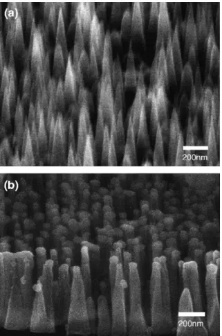
Fig. 1(a) and (b) show the surface morphology of the carbon nanotips and chromium carbide capped carbon nanotips by SEM observation, respectively. The growth parameters were chosen to grow the two kinds of nanotips to about 0.5 μm in length, to ensure the similar conditions for field emission me-asurements. The tip end of the carbon nanotips consists of several graphene layers which were less than 0.1 nm [3]. The chromium carbide capped carbon nanotips ends with crystalline nanoparticles which was about 40 nm and the diameter of the graphite right beyond the chromium carbide was a few nano-meters smaller than the chromium carbide. The chromium film was used as catalyst and was carburized into chromium carbide which was gradually lifted-off during growth. The diameter of
the two kinds of nanotips gradually increased toward the substrate via vapor–solid growth and may reach to about a hundred nanometers. The graphene layers of the nanotips body
Table 1
Brief list of the growth parameters for the materials Substrate H2/CH4 (SCCM) Bias (V) Growth time (min) Carbon nanotips Bare silicon 10/10 −100 30 Chromium carbide capped
carbon nanotips
Cr (20 nm) coated silicon
20/10 −150 15
Fig. 1. SEM images of (a) carbon nanotips and (b) chromium carbide capped carbon nanotips showing the surface morphology.
Fig. 2. The emission current density as a function of the electric field for (a) carbon nanotips and (b) chromium carbide capped carbon nanotips. The insets show the Fowler–Nordheim plot for each material.
Fig. 3. Plot of electric field with emission time for carbon nanotips and chromium carbide capped carbon nanotips. The current was set to a constant value of 1 mA. 1026 C.H. Hsu et al. / Thin Solid Films 515 (2006) 1025–1027
were perpendicular to the silicon substrate for both nanotips and were important to electron conduction.
The composition of the chromium carbide was most likely to be Cr7C3, which was identified from X-ray diffraction technique and diffraction patterns by transmission electron microscopy (TEM) [8]. However, weak peaks in the X-ray spectrum and visible diffuse rings could also be found in further analysis. According to the database, it suggested that the chromium carbide nanostructure may consist of Cr3C2, Cr23C6 or CrC, incorporated with large number of defects.
The relationship between the field emission current density and the electric field of the as-grown materials was shown in
Fig. 2. Due to the ultra-sharpness of the bare carbon nanotips, a low turn-on field (defined as the field required to emit a current density of 10 μA/cm2) of 1.4 V/μm can be reached. With chromium carbide, the tip structure exhibited a much higher turn-on field of 3.5 V/μm. Basically, the results differed from the surface appearances for which the field enhancement factor was greatly affected by the geometrical distribution. The sharp and less dense carbon nanotips also exhibited a comparatively reduced screening effect [10,11] due to a larger tip-to-tip spacing. The insets ofFig. 2(a) and (b) show respectively the Fowler–Nordheim (FN) relations. The linearity of the plot at the initial applied voltages before turn-on suggested the behavior of FN tunneling of the electron emission process.
Fig. 3shows the applied field as a function of emission time under constant current density which was set to 1 mA. Total emission time was 36,000 s, which was 10 h. The degree of stability of field emission was obviously quite different. The mean electric field for chromium carbide capped carbon nanotips was 8.02 V/μm with fluctuation less than 5% can be achieved. On the contrary, although the carbon nanotips showed a superior turn-on and thresholds field on the beginning of the test, the situation became chaotic after about 10,000 s. The oscillation was mainly due to the physical damage of the tip, which was confirmed by post observation of SEM. Instead, the chromium carbide capped carbon nanotips showed a smoother surface after the test without distinguishable major change. This phenomenon suggests that chromium carbide, known for its excellent oxidation resistance and hardness, effectively shields the carbon nanotips from destruction, which may be due to ion bombardment, heating and oxidation. Here we had assumed that the field emission current arise from the chromium carbide nanoparticles since the ends of the nanotips suffer a larger electric field and field enhancement, in contrast to the graphite body.
On the other hand, the extremely sharp end of the carbon nanotips would cause a great amount of current density to arise over the tip and generate a lot of heat due to ohmic heating. The uniformity of the capped carbon nanotips also benefited to the lifetime experiment while the disorderliness of the uncapped nanotips causes an unequal distribution of current and, as a result, sequential breakdown.
Chromium carbide has been synthesized and used for long periods of time, as hard coatings for tribological use. Therefore, the electric properties have not been totally explored. Reports
have shown that Cr3C2with conductivity of 68 × 106Ω− 1cm− 1 was used as conductive ceramics[12]and Cr7C3, which was the main structure of the chromium carbide nanoparticles in this study, may exhibit metallic behavior proposed from the chemical bonding structure[13]. In fact, defects in the chromium carbide may also provide a low energy conduction path[14]. In this case, the situation may be more complex since we were dealing with more than one material. The difference in work function between the carbides or between carbide and graphite could form ohmic and Schottky junctions which may limit the current. Even though the existence of the chromium carbide may not be favorable for electron conduction, the steady emission has shown importance for practical applications.
4. Conclusion
Field emission characteristics of carbon nanotips and chromium carbide capped carbon nanotips were investigated through I–V measurements and discussed. The electrical measurements showed a turn-on field of the bare carbon nanotips (1.4 V/μm) lower than the chromium carbide capped carbon nanotips (3.5 V/μm) for the as-grown samples. However, the bare carbon nanotips show very unstable field emission behavior while chromium carbide capped carbon nanotips reveal stable emission with current fluctuations less than 5%. The chromium carbide acts as a shield for the graphite and resists destruction due to heating, oxidation or ion-bombardment and contributed to steady emission.
Acknowledgement
This work was supported by the National Science Council of the Republic of China (NSC942216E009014).
References
[1] M. Ge, K. Sattler, Chem. Phys. Lett. 220 (1994) 192.
[2] J. Jang, S.J. Chung, H.S. Kim, S.H. Lim, C.H. Lee, Appl. Phys. Lett. 79 (2001) 1682.
[3] C.L. Tsai, C.F. Chen, L.K. Wu, Appl. Phys. Lett. 81 (2002) 721. [4] Shoushan Fan, Michael G. Chapline, Nathan R. Franklin, Thomas W.
Tombler, Alan M. Cassell, Hongjie Dai, Science 22 (1999) 512. [5] W.A. deHeer, A. Chatelain, D. Ugarte, Science 270 (1995) 1179. [6] W. Zhu, C. Bower, O. Zhou, G. Kochanski, S. Jin, Appl. Phys. Lett. 75
(1999) 873.
[7] C.L. Tsai, C.F. Chen, C.L. Lin, Appl. Phys. Lett. 80 (2002) 1821. [8] C.L. Tsai, J.H. Hsu, C.F. Chen, Appl. Phys. Lett. 82 (2003) 4337. [9] C.H. Hsu, S.C. Shi, C.F. Chen, Thin Solid Films 469–470 (2004) 131. [10] Jung Sang Suh, Kwang Seok Jeong, Jin Seung Lee, Intek Han, Appl. Phys.
Lett. 80 (2002) 2392.
[11] L. Nilsson, O. Groening, C. Emmenegger, O. Kuettel, E. Schaller, L. Schlapbach, H. Kind, J.M. Bonard, K. Kern, Appl. Phys. Lett. 76 (2000) 2071.
[12] C.T. Fu, J.M. Wu, A.K. Li, J. Mater. Sci. 29 (1994) 2671.
[13] D. Music, U. Kreissig, R. Mertens, J.M. Schneider, Phys. Lett., A 326 (2004) 473.
[14] Y. Show, F. Matsuoka, M. Hayashi, H. Ito, M. Iwase, T. Izumi, J. Appl. Phys. 84 (1998) 6351.
1027 C.H. Hsu et al. / Thin Solid Films 515 (2006) 1025–1027