CMOS
Low-Noise
Amplifier for
6-1
lGHz
MB-OFDM
UWB
Wireless Radio
System
Zhe-Yang
Huang',
Che-Cheng Huang2Dept.of Communication Engineering, National Chiao Tung University, Hsin-Chu, Taiwan
2Instrument
Technology Research Center, NARL, Hsin-Chu, TaiwanAbstract - This paper presents a low-power low-noise M ixer
amplifier (LNA) with switching bands for MB-OFDM Group-C /
andGroup-Dultra-wideband wireless radiosystem.TheLNA is designed and implemented in TSMC 0.18um RF CMOS process.
Simulation results show that power gain of12.4dB,inputand PLL DSP
output matching lower then -8.5dB and -14.5dB, and a r
-minimum N1F of 4.0dB can be achieved, while the power I
consumptionis 11.2 mWthrough1.8V powersupply. A D
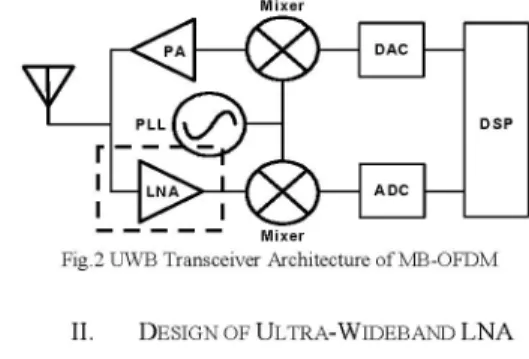
I. INTRODUCTION Fig.2UWBTransceiver Architecture of MB-OFDM
The Ultra Wide-Band (UWB) is a new technology for
wireless personal area networks (WPAN) which contains II. DESIGN OF ULTRA-WIDEBAND LNA manyadvantages ofhigh data transmission rate, low cost, and
low power consumption that is better than narrowband A. Wideband
Amplifier
Designwireless system.InFebruary, 2002,UWB system is approved A sketch of the wideband
amplifier
which containsinput
by
the Federal Communications Commission(FCC)
[1]*
matchmg network,main amplifier
and output buffer and that Although the UWB standard (IEEE 802. 15.3a) has not been is shown asFigure
3. Thespecification
of ultra-wideband defined which there are two specifications, DS-UWB and system is definedas3.1GHz-10.6GHz,
thereforeaverywideMB-OFDM,
and this papermainly design
for MB-OFDMbandwidth
input matching
network is necessaryin
the UWBtJWB system in the band of 6.0GHz-IlGHz for future LNA In this wideband
amplifier,
the mainamplifier
isapplications. The band definition of MB-OFDM is illustrated including the low-noise amplifier and switching, capacitors, in
Fig.
1 which extended from 3168MHzto10296MHz,
and and theswitching capacitors
aredesign
forswitching
groupsthe bandwidth of MB-OFDM is
containing Group-A,
for MB-OFDM UWBwireless radio
system. For Group-C andGroup-D.; and theproposedLNAisdesignfor measurementconsideration,
theoutputimpedance
isalways
Group-C and Group-D. The Group-B is not considered indesigned
for 50 ohms i the output buffer. Thedesign
current UWB system which causedbythe U-NII band and g
WLAN (IEEE 802.11a). considerationsreturnloss, power gain, and noise figure (NF), linearityoflow-noise amplifier are mainly in input
(P1dB,
IIP3) and power consumption, but thereare some trade-offGROUPA GROUP B GROUP C GROUPD
between theseimportantcharacteristics.
iBand Band Band Band Ban.d Ban.d Ban.d Band Band Band Band Ban.d Ban.d #1
#2 #3 #4 #5 #6 #7 #8 #9 #10 #11 #12 #13
4
_
~~~~~~~~~~~~~~~~0
RF IN
I
I
RF OUT
3432 3960 4488 5016 5808 6336 6864 7392 7920 8448 8976 9504 10032 |Matchingf LN
MHzll xnu MHzll Ng-L MHz MHzll xnu MHzll MHzll xnu MHz MHz MHz NetworkLNATttXI
Fig. IBand Definition of MB-OFDM
2) T~~~~~CslCs2 Cs3 Buffer ()
In RF wireless receiver, LNA is one of themost critical
building blocks caused by the noise figure is dominated inI't w W3 stage of the receiver that is illustrated inFig. 2. For LNA
design, there are many trade-off between different - - -
-specifications. For example, the power gain affects noise Fig.3WidebandAmplifier
figure, the die areaaffect cost, and the power consumption
affects thebatterylife. B. Proposed Low-Noise
Amplifier
IntheFigure 4, the proposed low-noise amplifier comprises the input matching network which is implemented by the
588
1-4244-0797-4/07/$20.00
( 2007 IEEEChebyshev Filter
[3]
where are Li, Ci, L2, C2, Lg, Ls and Cgsi; RsLl
Cl
Zins
Ls Cgsi the main amplifier is containing Mi, M2, LLI, Csl, Cs2, Cs3,SWi, SW2and SW3; the output buffer is the M3; and Lsp is '1
the series peakinginductor,the Cdcl, Cdc2 are DC blocking 5
capacitors. The voltage gain of cascade amplifier is Av which j Vs L2 T RL is described in (1), where gmi is the transconductance of Mi, Zin
LLI is the loading of the cascode amplifier Ccaps is the total __
capacitor which including the switching capacitor and Fig.6 Input Matching Network in Small Signal Models
parasitic capacitors. And Zin is expressed in equation (3), B(s) is the equivalent impedance of Li, L2, Ci and C2; Zin is an impedance of a
6th
VDD orderband-pass filter which is too complicated to express inF,g VDD theequation; and the equation (3) is the basic form.
VDD
_El
I
I
T; |LL1SF,
-Zns
=9~~~~~in
sL
SCC+S
+ mlLs
sg + +TLs
(2)
gsl
gsl gsI T1
M3 RF_OUT Csl s2Cs3
Cd
Zin
=
(sLI
+
)
(sL2
)
(sLg +
+
w,LS)
Lspcd~1
s RF_INLI
CITC2
_S _S_1W =B(s)II(sL + 1 +Ls)
Lg~~ ~ ~ ~
]g SgsiI OS ()DI~.7~i
1MI -L2
(3) D. SeriesPeaking
VBiasFig.4ProposedLow-NoiseAmplifier
vWhen
designing
awideband
amplifier,
the mostcritical
problem is the bandwidth limited by large capacitance whichA = -s9 1(1) affects the
high frequency
response.Thus,
thehigh frequency
1+
g,1Ls
+s(LLICcas
+ L LCcp
) response is difficult to reach higher frequency. Therefore,series
peaking
is a goodsolution
to solve theimportant
C. Wideband InputMatching Network problem that is adding inductance Lsp alongthe RF path.The wideband
input matching
networkarecontaining
LiFigure
7 illustrates thefrequency
response with seriesCI, L2, C2, Lg,LsandCgsIwhichis shown in
Figure
5;andpeakig
inductor, the inductor raise thehigh frequency
isinput impedance
fromthe source terminal. The modified response. In the other way, seriespeaking
is also could beequivalent
circuit with smallsignal
models is shown in the viewed in timeconstantissue. And the timeconstantwithout Fig. 6. The equivalent input impedance Zins is expressed in Eq.series peaking
is shown in (4); adding the inductor Lsp, and 2whereRL
=cLs.
RLisalways design
for 50 ohms;Lg
thenewtimeconstantisderivedas(5).
TheCeq
ismodifiedas(2),Cgs
I designtocancel each other in imageimpedance.
a newcapacitor, and the capacitance is alsosmaller; forthisand
Cgsl1
are design to cancel each other in imageimpedance. reason, the time constant is becoming reduced.Zins 20- I I I RFIN LI C1 TV ml v V
('V~~~~~~~~~~~~~~~~~~~~~~~~~~~~~~~
_ _ ~~~~~~~~~~~~~~~-*-Q.QQnH L- --O--.59nH . -. -_ n .OnFig.5 Input Matching Network -- 1.36nH
SG 6G 7G SG 9G lOG 11G 12G
Frequency
Fig.7Inductance of SeriesPeaking
1
eRC
rq
Cgs2
(4)
2--Band#12,13
--- -- -- 11
Band#8, 9
where Ceq = (Cgs2 1lCeaps) ' -4- ._\ . -v Band#6, 7
req 4-1+( m m 2 )r 2 ] o o ---T---,----
I---n---I--n---I---2=RC
=req.*Ceq
(5) -12- -- ------>~~~---64- ---~~
where
C = 2spcaps-10-
2 .z'2
=RC
(C00 rWcaps ° 2.OG 4.0G 6.QG 8.oGS 10.OG 12.OG
Frequency
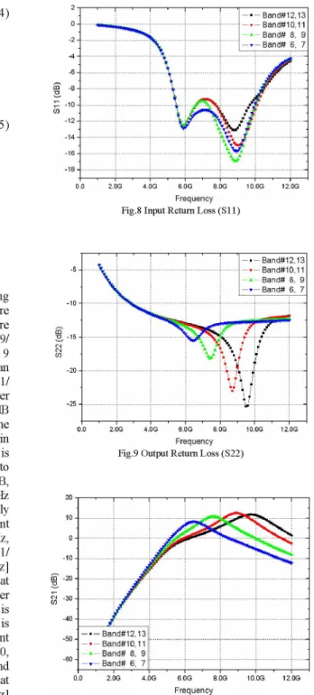
Fig.8 Input Return LOSS(Si11)
req = [1 +
(g,12
+ gmb2
)'o2 ]iOl
+
rO2
III. SIMULATION RESULTS -.-Band#12,13
\ ~~~~~~~~BandX8, 9
The simulation results of the proposed
UJWB
LNA using 13 .^ ---Band# 6,7 Agilent ADS2005A simulator are given in Figure 8 to Figure12. In Figure 8 that can be seen the input return loss (511) are _
lower than -12.7dB/-9.5dB/-1 1.3dB/-8.5dB (Band #6,
7/1#8,
9/ r~5 4 #10, 11/ #12, 13) between 6.0GHz to 10.6GHz. In Figure 9 -;that can be seen that the output return loss (S22) are lower than 203 7 -14.5dB/-14.8dB/-15.8dB/-15.6dB (Band #6, 7/#8, 9/#10, 11/
#12, 13)between 6.GHzto 10.6GHz, respectively. The power gain whose peak value are 8.3dB, 10.8dB, 12.4dBandl11.7dB ; ; ; ; .
at 6.5GHz, 7.5GHz, 8.9GHz and 9.7GHz which covers the
0o20G
4.0G 60G 80G 100G 12.0GGroup-C and Group-D ofthe MB-OFDM, and that is shown in Frequency
Figure 10. In Fig. 11, it can be seen that the noise figure is Fig.9Output Return Loss (S22) below 4.9dB, 4.3dB, 4.1dB and 4.5dB between 6.0GHz to
10.6GHz and the minimum noise figure are 4.8dB, 4.1dB,
4.0dB and 4.0dB at 6.6GHz, 7.5GHz, 8.8GHz and 9.5GHz 20 -'---r--'---r
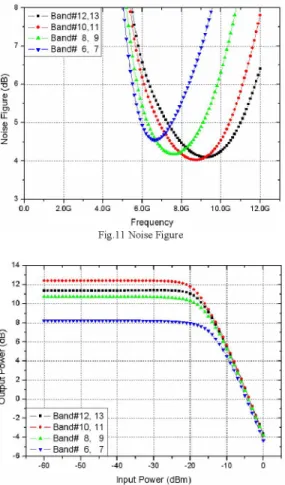
I--(Band #6, 7/ #8, 9/ #10, 11/ #12, 13) through 1.8V supply 0voltage. In Fig. 12, the input-referred 1dB compression point (IPldB) is -15dBm, -17dBm, -18dBm and -17dBm at 6.5GHz, o
7.5GHz, 9.0GHz and 10.0GHz (Band #6, 7/ #8, 9/ #10, 11/ 10 ---g---16---#12, 13). Third-Order Input Intercept Point (IIP3)
[528MHz]-t
at6336MHz and6864MHzis-4dBm
(Band
7);[10M
#6, Hz] at---20---
--I--- ----I---I---6864MHz and 6874MHz is -3dBm (Band #6, 7); Third-Order 30 ;
Ceq~~~~~~~~~~~~~~~~~~~~~~~~~~~~~~~~~~~~~~~~l
Input Intercept Point [528MHz] at 6864MHz and 7392MHz
is--2dBm (Band #8, 9);[10MHz] at 7392MHz and 7402MHz is ~ 3
-ldBm (Band #8, 9); Third-Order Input Intercept Point 5Q
-Band#1O,
11 [528MHz] at 8448MHz and 8976MHz is +ldBm (Band #10, 60Band# 8,
9 11);[10MHz] at 8448MHz and 8458MHz is +ldBm (Band --ad#10, 11); Third-Order Input Intercept Point
[528MH-Iz]
at 00 2OG 4.0G 60G 8.0G 10.OG 120G6336MHz and 6864MHz is +ldBm (Band #12, 13),[10MHz] Frequency
at 6336MHz and 6346MHz is +ldBm (Band #12, 13); The
Fig.
1PowerGain(S21)
power consumption is 11.2mW through 1.8V supply voltagewhich neglects the power of output buffer. And the layout is illustrated inFigure 16.
8
-*-Band#12,13'
Band 1 6,7 #8,9 #10,11 #12,13 -E-Band#1O,11 FI 511I (dB) < -12.7 < -9.5 < -11.3 < -8.5 Band# 8, 9 Band# 6, 7 S22 (dB) <-14.5 <-14.8 <-15.8 <-15.6 S21(dB) 5.9-8.3 8.7-10.8 9.5-12.4 8.7-11.7 - S21 Max.(dB) 8.3 10.8 12.4 11.7 * X;5;m m . Working Bandwidth (GHz) 6.0-7.2 7.0-8.2 8.1-9.3 8.7-10.6 LLm \ -++ t. _ NF(dB) 4.8-4.9 4.1-4.3 4.0-4.1 4.0-4.5 IP1 dB(dBm) -15 -17 -18 -17 X i IIP3(dBm) [lOMHz] -3 -1 +1 +1 IIP3(dBm) [528MHz] -4 -2 +1 +1 PowerConsumption (mW) 11.2 11.2 11.2 11.20.0 2.OG 4.OG 6.OG 8.OG 1MG 12.OG Table.1Performance Conclusions
Frequency Fig.1I Noise Figure
14 ACKNOWLEDGMENT
12- *++++++ +...++ X@ ,. The authors would like tothank the chip implementation center(CIC)for technical support.
10-._
i..
O , , A ~~~~~~~~~~~~~REFERENCES
[1] FCC,"FinalRule of the FederalCommunications Commission, 47 CFR
^ . t
~~~~~~~~~~~~~~~~~~Part
15,Sec. 503", Federal Register, vol. 67,no. 95,May 2002.2 -*-Band4l21v,13 9 [2] _
-9BandS1O, 11 4Cellll)6
~4 Band# 8, 9. . _
e
TBand#
6, 7 . [3] Andrea Bevilacqua, and Ali M. Niknejad," An Ultrawideband CMOS -60 -50-40-30 -20 10 0~~~Low-Noise
Amplifier for 3.1-10.6-GHz Wireless Receivers "IEEEInputPower~dBm) JOURNAL OF SOLID-STATE CIRCUITS, Vol. 39, No.
Fig. 12 Input-Referred 1dB Compression Point (P1dB)12p25926De204
[4] Chang,C.-P.; Chuang, H.-R., '0.18 um 3-6 GHz CMOS broadband LNA for UWB radio", ElectronicsLetters, Volume 41, Issue 12, June 2005
IV. CONCLUSIONS Page(s):33-34.
A CMOSlow-nise aplifir is esignfor M-OFDM [5] Chang-Wan
Kim, Min-Suk
Kang, Phan Tuan Anh, Hoon-TaeKim,
andUltra-Wideband wireless radio system which using the Sang-Gug Lee, 'An Ultra-Wideband CMOS LowxNoise Amplifier for
switching capacitor technique to implement the multi-group 3-5-GHz UWB System", IEEE JOURNAL OF SOLID-STATE applications. The simulation results show that the proposed CIRCUITS, Vol. 40, No.2,pp.544-547,Feb. 2005.
UWB LNA gives 8.3dB/10.8dB/12.4dB/1 1.7dB (Band#6,7/ [6] Chih-Fan Liao; Shen-IuanLiu, "A broadband noise-canceling CMOS #8, 9/ #10, 11/ #12, 13) maximum power gain between LNA for 3.1-10.6-GHz UWB receiver, Custom Integrated Circuits 3.1GHz to 10.3GHz while consuming 11.2mW though 1.8V Conference, 2005. Proceedings of the IEEE 2005, 18-2t1 Sept. 2005
power supply. Page(s):161-164.
|Paper |CircuitTopology TTechnology |Sll(dB) | 22(dB) T521(dB) |BW(GHZ) |Gmax(dB) TNF(dB) TNFmin(dB) |Pdiss(mW)|
[4] 13-stagescomm.-sourceT0.l8umCMOSI <-12.2 <-10.1 T13.5-15.81 3.0-6.0 15.7 T4.7-6.7 T 4.7 59.4
[5] |2-stageshunt-peaked
t0.l8um
CMOS |<-9.5 |<-8.1 T15.3-18.0 |3.1-5.0 |18.03 T2.7-3.1 T 2.7 |25.9 |[6] 3-stages shunt-peaked 0.18um CMOS <-7 < -12 6.7-9.7 1.2-11.9 9.7 4.5-5.1 4.5 20.0
This Work Switching Capacitors 0.1l8umCMOS < -8.5 <-14.5 5.9-12.4 6.0-10.6 12.4 4.0-4.9 4.0 11.2 Table.2 PerformanceComparisons