642 IEEE PHOTONICS TECHNOLOGY LETTERS, VOL. 23, NO. 10, MAY 15, 2011
Light Output Enhancement of UV Light-Emitting
Diodes With Embedded Distributed Bragg Reflector
Bo-Siao Cheng, Ching-Hsueh Chiu, Ming-Hua Lo, Yun-Lin Wu, Hao-Chung Kuo, Tien-Chang Lu,
Yuh-Jen Cheng, Shing-Chung Wang, and Kuo-Jui Huang
Abstract—We demonstrate the output power enhancement of
ul-traviolet light-emitting diodes (UVLEDs) by epitaxial lateral over-growth (ELOG) on a distributed Bragg reflector (DBR) patterned substrate. The patterned DBR mesas are used as ELOG masks to improve material quality as well as reflectors to enhance the light output coupling. Compared with the conventional UVLEDs, the surface pit density of UVLEDs at regions right above embedded patterned DBR were reduced from to cm . The improved light extraction efficiency is verified by ray tracing simulation. The luminous intensity of this novel structure is en-hanced by 75% compared to that of reference UVLED structure at the wavelength 390 nm.
Index Terms—Distributed Bragg reflector (DBR), ultraviolet
light-emitting diodes (UVLEDs).
I. INTRODUCTION
G
ALLIUM nitride (GaN) based light emitting diode (LED) has attracted great interest due to its importance in lighting applications [1], [2]. GaN based LED has become the most efficient lighting device. The device is often heteroepi-taxially grown on a foreign substrate, for example sapphire due to the lack of GaN substrate. The as grown GaN epitaxial layer typically has fairly high threading dislocation density due to large lattice constant mismatch between GaN and sapphire. These defects are nonradiative recombination centers and are detrimental to optoelectronic device performance. Another problem for GaN LED is its large refractive index, which allows only a small light escaping angle. Significant part of emitted light is trapped by total internal reflection resulting in low light extraction efficiency. Researchers are actively investigating various approaches to reduce defect density and improve light extraction efficiency.A very well known method to reduce defect density is the epitaxial lateral overgrowth technique (ELOG) [10], [11]. Strips of SiO mask are deposited on GaN epi-surface, followed by Manuscript received August 21, 2010; revised February 01, 2011; accepted February 19, 2011. Date of publication February 28, 2011; date of current ver-sion April 27, 2011. This work was supported by the National Science Council of the Republic of China in Taiwan under Contract NSC 95-2221-E-009-282 and Contract NSC 95-2752-E-229-007-PAE.
B.-S. Cheng, C.-H. Chiu, M.-H. Lo, Y.-L. Wu, H.-C. Kuo, T.-C. Lu, and S.-C. Wang are with the Department of Photonics, National Chiao Tung Uni-versity, Hsinchu 30010, Taiwan.
Y.-J. Cheng is with the Research Center for Applied Sciences, Academia Sinica, Taipei 11529, Taiwan.
K.-J. Huang is with the R&D Division, Tyntek Corporation, Hsinchu 300, Taiwan.
Color versions of one or more of the figures in this letter are available online at http://ieeexplore.ieee.org.
Digital Object Identifier 10.1109/LPT.2011.2121057
epitaxial growth. The growth starts from window regions and grows vertically as well as laterally to cover the SiO strips until obtaining planar surface over whole wafer. The lateral growth bends the threading dislocation propagation direction and results in significantly lower defect density over the mask than in the window region. For light extraction efficiency improvement, various surface roughening processes have been demonstrated and shown significant improvement in light extraction efficiency [3]–[7]. Photonic crystal (PC) structure has also drawn great interests in light extraction efficiency en-hancement application [8], [9]. Here, we demonstrate an ELOG technique to simultaneously improve both material quality and light extraction efficiency. Patterned DBR mesas were fabri-cated on a GaN substrate and used as masks for epitaxial lateral overgrowth (ELOG) and photon reflector for enhancing light output coupling. The DBR reflector is intentionally designed to have high reflectivity at LED emission wavelength so that the emitted light toward GaN-sapphire interface is reflected back to the front surface. A ray-tracing simulation was discussed to investigate the mechanism of light output enhancement.
II. EXPERIMENT
The ultraviolet LED (UVLED) samples were grown on c-plane sapphire substrates by a low pressure metal organic chemical vapor deposition (MOCVD) system. The fabrication flowchart of UVLEDs with embedded patterned distributed Bragg reflector (DBR) was shown in Fig. 1. First, a 30-nm-thick low-temperature GaN nucleation layer was grown on sapphire substrate, followed by a 1- m-thick undoped GaN layer. Then, 9.5 pairs of HfO SiO multiple dielectric layers were deposited on the GaN substrate. The thickness of HfO and SiO layer was 53 nm and 69 nm, and the refractive index at 390 nm wavelength was 1.98 and 1.46, respectively. The multiple dielectric layers were patterned by a conventional lithography and liftoff technique to form circle-shape masks with the diameter of 5 m. A 3- m-thick Si-doped n-GaN layer was regrown from the region without masks and laterally overgrown masks till forming a flat surface, followed by the deposition of a InGaN/GaN multiple quantum well (MQW) active region with emission wavelength designed at 390 nm. On top of the active region is a 50-nm-thick Mg-doped p-AlGaN electron blocking layer and a 0.2- m-thick Mg-doped p-GaN cladding layer. Subsequently, m diode mesas are defined by chlorine-based reactive ion etching. An indium tin oxide (ITO) film (250 nm) was deposited on p-GaN layer as a transparent conductive layer. The Cr/Pt/Au (50 nm/50 nm/ 2500 nm) metal contacts were deposited for p- and n-contact 1041-1135/$26.00 © 2011 IEEE
CHENG et al.: LIGHT OUTPUT ENHANCEMENT OF UVLEDs WITH EMBEDDED DBR 643
Fig. 1. Fabrication flowchart of DBR embedded UVLEDs.
Fig. 2. Reflectivity spectrum of (a) HfO2 and SiO2 9.5-pairs DBR before MOCVD baking and (b) the DBR after MOCVD 1000 C backing.
pads. An UVLED without the embedded DBR and an UVLED with embedded SiO2 were also fabricated for comparison.
III. RESULTS ANDDISCUSSION
Fig. 2(a) shows the reflectivity spectrum of the 9.5-pair HfO SiO DBR, indicating that the maximum reflectivity was 98.4% at the wavelength of 390 nm. The reflectivity spectrum of the DBR after MOCVD 1000 C baking was shown in Fig. 2(b). It reveals the maximum reflectivity was degraded to 95.4% and the center wavelength was shifted to 356 nm. The reflectivity was 88.9% at the emission wavelength 390 nm. In DBR structure, we inferred that the refractive index of the HfO2 dielectric layer was decreased after MOCVD 1000 C baking. So that, the center wavelength of DBR reflectance spectrum was shifted with the refractive index decrease of the dielectric layer.
Fig. 3. (a) SEM images of HfO2 and SiO2 9.5-pairs DBR; (b) enlarged (a).
Fig. 4. CL images of (a) reference UVLEDs surface and (b) DBR embedded UVLEDs surface after epitaxial growth by MOCVD.
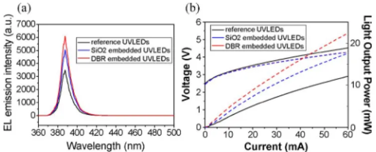
Fig. 5. (a) EL emission spectrum. (b) Measured – – characteristics of the fabricated UVLEDs.
Fig. 3(a) shows a scanning electron microscope (SEM) cross section micrograph of the 9.5-pair HfO SiO DBR before mesa patterning fabrication. Fig. 3(b) is an enlarge view of Fig. 3(a).
Figs. 4(a) and 4(b) show the cathodoluminescent (CL) im-ages of the surfaces of reference and DBR embedded UVLEDs. The dark spots are believed to be originated from the threading dislocation defects terminated at the surface. The defects are strong nonradiative recombination centers therefore showing low CL intensity. The deduced defect densities of the reference
and DBR embedded UVLEDs are and cm ,
respectively. The defect density of DBR embedded UVLED is significantly improved by 36% compared to that of reference UVLED sample.
Fig. 5(a) shows EL emission spectrum of the reference, SiO2 and DBR embedded UVLEDs. It is worthy of note Fig. 5(a) that the emitting spectrum of the SiO2 and DBR embedded UVLEDs share the same characteristics with the reference UVLED which implies that the fabricated embedded structure mainly works to enhance light output from the UVLED. All the emission wavelength of the reference, SiO2 and DBR em-bedded UVLEDs are 390 nm. Fig. 5(b) exhibits the light output power and operation voltage as a function of forward current ( – – curve) for the reference, SiO2 and DBR embedded
644 IEEE PHOTONICS TECHNOLOGY LETTERS, VOL. 23, NO. 10, MAY 15, 2011
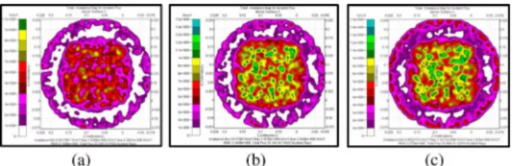
Fig. 6. Candela maps of (a) reference UVLEDs, (b) SiO2 embedded UVLEDs, and (c) DBR embedded UVLEDs.
UVLEDs. The output power of DBR embedded UVLED is significantly enhanced. The forward voltage is also slightly reduced. At the driving current of 20 mA, the output power of reference, SiO2 and DBR embedded UVLEDs are 5.06, 7.34 and 8.86 mW, respectively. The optical power of SiO2 and DBR embedded UVLED have very significant 45% and 75% improvement compared with reference UVLEDs, respectively. We attribute this enhancement to the improvement in material quality from ELOG growth and light output coupling from embedded DBR. At the same driving current, the forward voltages of reference, SiO2 and DBR embedded UVLEDs are 3.52, 3.44 and 3.45 V, respectively. The lower forward voltage can be attributed to the reduction in material defects, which are carrier scattering centers. The reduction in scattering sites results in lower forward voltage.
In order to investigate the factors contributing to light output enhancement in DBR embedded UVLED, ray-tracing models of UVLEDs with and without embedded DBR were used to investigate the light output coupling enhancement. The com-mercial ray-tracing software, which employs the Monte-Carlo algorithm, is used to obtain trajectory of ray-tracing, en-hancement efficiency, and spatial intensity distributions of radiometric and photometric data. The detector model was built in the shape of integrating sphere and used to record the emission flux of UVLED model. The candela maps show the intensity distribution of the detector model. Fig. 6(a), (b) and (c) show the candela maps of reference, SiO2 and DBR embedded UVLEDs. The simulation results indicate that the light ex-traction efficiency of SiO2 and DBR embedded UVLEDs are significantly enhanced by 48% and 61% compared with refer-ence UVLEDs, respectively. The central intensity of Fig. 6(c) was greater than that of Fig. 6(a). It shows that the downward light is reflected by embedded DBR mesas and consequently contributes to the power enhancement. This simulation indi-cates that the output power enhancement is mostly contributed by the underlying DBR mesa reflectors.
IV. CONCLUSION
In summary, the UVLED with embedded DBR were fabri-cated by ELOG technique. The luminous intensity of this novel structure is greatly enhanced by 75% compared to that of con-ventional UVLED structure. The improved light extraction ef-ficiency can be further supported by ray-tracing simulation re-sults. The simulation shows that the output power enhancement is mostly contributed by the light output coupling improvement from the embedded DBR reflectors while the improvement in material quality from ELOG only contributes a smaller fraction.
REFERENCES
[1] S. Nakamura, T. Mukai, and M. Senoh, “Candela-class high-brightness InGaN/AlGaN double-heterostructure blue-light-emitting diodes,” Appl. Phys. Lett., vol. 64, pp. 1687–1689, 1994.
[2] G. B. Stringfellow and M. G. Craford, . Boston, MA: Academic, 1997.
[3] J. K. Sheu, C. J. Pen, G. C. Chi, C. H. Kuo, L. W. Wu, C. Chen, H. Chang, and Y. K. Su, “White-light emission from InGaN–GaN multi-quantum-well light-emitting diodes with Si and Zn codoped active well layer,” IEEE Photon. Technol. Lett., vol. 14, no. 4, pp. 450–452, Apr. 2002.
[4] I. Schnitzer, E. Yablonovitch, C. Caneau, T. J. Gmitter, and A. Scherer, “30% external quantum efficiency from surface textured, thin-film light-emitting diodes,” Appl. Phys. Lett., vol. 63, no. 16, pp. 2174–2176, 1993.
[5] Y. J. Lee, H. C. Kuo, S. C. Wang, T. C. Hsu, M. H. Hsieh, M. J. Jou, and B. J. Lee, “Increasing the extraction efficiency of AlGaInP LEDs via n-side surface roughening,” IEEE Photon. Technol. Lett., vol. 17, no. 11, pp. 2289–2291, Nov. 2005.
[6] Y. J. Lee, H. C. Kuo, T. C. Lu, and S. C. Wang, “High light-extrac-tion GaN-based vertical LEDs with double diffuse surfaces,” IEEE J. Quantum Electron., vol. 42, no. 12, pp. 1196–1201, Dec. 2006. [7] Y. J. Lee, J. M. Hwang, T. C. Hsu, M. H. Hsieh, M. J. Jou, B. J. Lee,
T. C. Lu, H. C. Kuo, and S. C. Wang, “GaN-based LEDs with Al-de-posited V-shaped sapphire facet mirror,” IEEE Photon. Technol. Lett., vol. 18, no. 5, pp. 724–726, Mar. 1, 2006.
[8] J. J. Wierer, M. R. Krames, J. E. Epler, N. F. Gardner, M. G. Craford, J. R. Wendt, J. A. Simmons, and M. M. Sigalas, “InGaN/GaN quantum-well heterostructure light-emitting diodes employing photonic crystal structures,” Appl. Phys. Lett., vol. 84, pp. 3885–3887, 2004. [9] T. N. Oder, K. H. Kim, J. Y. Lin, and H. X. Jiang, “III-nitride blue and
ultraviolet photonic crystal light emitting diodes,” Appl. Phys. Lett., vol. 84, pp. 466–468, 2004.
[10] A. Kaschner, A. Hoffmann, C. Thomsen, F. Bertram, T. Riemann, J. Christen, K. Hiramatsu, T. Shibata, and N. Sawaki, “Optical mi-croscopy of electronic and structural properties of epitaxial laterally overgrown GaN,” Appl. Phys. Lett., vol. 74, p. 3320, 1999.
[11] J. Holst, A. Kaschner, A. Hoffmann, P. Fischer, F. Bertram, T. Riemann, J. Christen, K. Hiramatsu, T. Shibata, and N. Sawaki, “Time-resolved microphotoluminescence of epitaxial laterally over-grown GaN,” Appl. Phys. Lett., vol. 75, p. 3647, 1999.