國立交通大學
光電工程學系碩士班
碩士論文
主動式液晶透鏡應用於裸眼立體顯示器
Active-TFTs Liquid Crystal Lens for
Multifunctional 3D Displays
研究生:王柏皓
指導教授:謝漢萍 博士
黃乙白 博士
主動式液晶透鏡應用於裸眼立體顯示器
Active-TFTs Liquid Crystal Lens for Multifunctional 3D Displays
研究生:王柏皓 Student:Po-Hao Wang
指導教授:謝漢萍 Advisor:Han-Ping D. Shieh
黃乙白 Yi-Pai Huang
國立交通大學
光電工程學系碩士班
碩士論文
A ThesisSubmitted to Institute of Electro-Optical Engineering College of Electrical and Computer Engineering
National Chiao Tung University in partial Fulfillment of the Requirements
for the Degree of Master
in
Electro-Optical Engineering June 2012
Hsinchu, Taiwan, Republic of China
中華民國一百零一年六月
i
主動式液晶透鏡應用於裸眼立體顯示器
碩士研究生:王柏皓 指導教授:謝漢萍教授
黃乙白副教授
國立交通大學 光電工程學系碩士班
摘 要
為了得到更自然的立體影像,近年來已有許多專家及廠商投入立體顯示器的 發展。大多數立體顯示器使用固定式的光學元件,但此種顯示器僅能提供 3D 影 像,無法提供 2D 影像。因此,可切換 2D、3D 影像顯示器的發展便顯得重要。本論文提出的主動式液晶透鏡(Active-TFTs Liquid Crystal Lens)可應用 於 2D、3D 影像的切換,也可應用於 3D 旋轉式螢幕,又或者是區域性的 2D、3D 切換。此篇將藉由半導體特性形成的開關,以及高阻值材料層的液晶透鏡,來達 到區域性的 2D、3D 切換。透過閘極與源極輸入電壓,便可決定哪一個透鏡的中 央電極將被充電。關閉輸入電壓後,若與兩旁電極無壓差,則無透鏡效果,反之 亦然。主動層以及液晶層的電性將會影響充放電的時間,其中又以漏電流最影響 放電時間,進而影響液晶透鏡的持續時間。利用退火得到好的主動層電性,再利 用儲存電容延長放電時間,如此一來便能達到區域性的 2D、3D 切換,使得未來 立體顯示器功能上有更多發展的可能性。
ii
Active-TFTs Liquid Crystal Lens for
Multifunctional 3D Displays
Student: Po-Hao Wang Advisor: Dr. Han-Ping D. Shieh Dr. Yi-Pai Huang
Institute of Electro-Optical Engineering National Chiao Tung University
Abstract
Recently, many researchers invest in developing 3D display technology to produce much natural images from displays. Since most of display applications use the fixed optical components to display 3D images, the 2D images cannot be provided by the same displays. Thus, a 2D/3D switchable display is needed.
In this thesis, we designed an Active-TFTs Liquid Crystal Lens for multifunctional 3D display such as, 2D/3D switchable、3D rotatable、2D/3D localized. For the on/off switch characteristics of semiconductor and high resistance liquid crystal lens, the 2D/3D localized LC lens could be obtained. By applying individual voltage on gate and source electrodes, the decided drain electrodes will be charged. Once turning off the applying voltage, if there is no potential difference between two electrodes, there won’t have lens effect, and vice versa. The electrical properties of LC layer and active layer will affect the charging and holding state. The annealing process and storage capacitor can enhance the lens holding time. This makes the Active-TFTs LC lens become more potential for applying in 3D display such as 2D/3D localized.
iii
誌 謝
能順利完成本篇論文,首先要感謝指導教授謝漢萍教授以及黃乙白教授。感 謝老師帶領進入顯示器領域,並且在求學與研究過程中的指導與資源提供。在生 活上,更從兩位教授身上學習到以和為貴的處事方法以及幽默的對談,在此向兩 位教授致上最誠摯的謝意。 兩年在實驗室裡的日子裡,感謝一起做實驗的陳致維學長,學長教導了很多 事情與概念,在遇到研究瓶頸時能相互討論、帶著我向前邁進,對論文及實驗有 很大的幫助。此外,精益學長、國振學長、育誠學長、志明學長、博元學長的討 論與相處也讓我獲益匪淺;也特別感謝在專題生時期帶我一起做實驗的志堯學長, 做實驗難免聊天,學長分享的人生經驗與待人處事的態度,讓我思考、讓我成長、 讓我學習。此外也感謝實驗室的其他人,讓我知道時間的可貴,同樣兩年可以選 擇自我進步,也可以虛度光陰。 最後,還有許許多多為了保護隱私而無法透露的親友、師長、夥伴、朋友, 有大家的支持才有今日的我,在逃避時給予勇氣、在虛弱時給予鼓勵、在寂寞時 給予溫暖、在迷失時給予方向,你們是我內心動力的來源,也是我夢想的起源。 但願未來的每一天都有你們的陪伴,在登上世界舞台那刻,能看見我發光發熱, 把榮耀歸還於你們每一個人。謝謝。iv
Table of Contents
摘 要 ... i
Abstract ... ii
誌 謝 ...iii
Figure Captions ... vi
List of Tables ... ix
Chapter 1 ... 1
1.1 Preface ... 1 1.2 Principle of 3D image ... 2 1.3 3D display technologies ... 5 1.3.1 Stereoscopic displays ... 5 1.3.2 Auto-stereoscopic displays ... 61.3.3 Multiplexed 2D type displays ... 7
1.3.4 2D/3D switching methods ...10
1.4 Introduction to liquid crystal ...14
1.5 Liquid crystal lens (LC lens) ...17
1.6 LC lens with 2D/3D switching ...20
1.7 Motivation and objective ...21
1.8 Organization ...22
Chapter 2 ... 23
2.1 Introduction ...23 2.2 Fabrication processes ...23 2.3 Measurement system ...33 2.4 Summary ...34Chapter 3 ... 35
3.1 Introduction of HR-TFT LC lens ...35v
3.3 Operation odf HR-TFT LC lens ...40
3.4 Summary ...42
Chapter 4 ... 43
4.1 Introduction ...43
4.2 Measurement results ...43
4.2.1 Reconstruction of the HR-TFT LC lens ...44
4.2.2 Analysis of the electrical properties ...45
4.2.3 Operating voltage and response time ...48
4.3 Summary ...50
Chapter 5 ... 52
5.1 Conclusions ... 54
5.2 Future work ...55
5.3.1 Holding time enhancement ...56
5.2.2 Passive layer on a-IGZO film ...57
5.2.3 Summary ...57
vi
Figure Captions
Fig. 1- 1 History of display technology. ... 1
Fig. 1- 2 Horizontal disparity. ... 2
Fig. 1- 3 Picture illustrating depth cues. ... 3
Fig. 1- 4 Vergence angle. ... 3
Fig. 1- 5 Accommodation. ... 4
Fig. 1- 6 Depth cues ... 4
Fig. 1- 7 Classification of 3D display technology... 5
Fig. 1- 8 Shutter type 3D display. ... 6
Fig. 1- 9 Concept of the time and spatial multiplexed type ... 7
Fig. 1- 10 3D display based on sequentially switching backlight with focusing foil. .. 8
Fig. 1- 11 Spatial multiplexed displays: parallax barrier. ... 8
Fig. 1- 12 Spatial multiplexed displays: lenticular lens array ... 9
Fig. 1- 13 Slanted lenticular lens 3D display with multi-view by the Philips Company ...10
Fig. 1- 14 2D/3D switching display with active parallax barrier. ... 11
Fig. 1- 15 Polarization activated micro-lens ...12
vii
Fig. 1- 17 Electric-field-driven LC lens (ELC lens). ...13
Fig. 1- 18 Principle of the MeD-LC lens. ...14
Fig. 1- 19 Schematic diagram showing the orientation of rod-like molecules ...14
Fig. 1- 20 Geometry to calculate refractive index change with liquid crystal molecule orientation……….…15
Fig. 1- 21 Conventional lens. ...17
Fig. 1- 22 GRIN lens ...17
Fig. 1- 23 The geometry of the focused GRIN Lens………18
Fig. 1- 24 LC cylindrical lens ...19
Fig. 1- 25 (a) Lens off (b) Lens on. ...20
Fig. 1- 26 Sketch of high-resistance TFT liquid crystal lens ...22
Fig. 2- 1 Fabrication steps...24
Fig. 2- 2 Schematic picture of step1 and step 5. ...25
Fig. 2- 3 The mask pattern of gate substrate and bottom lock. ...26
Fig. 2- 4 Flow of fabricating ITO electrode ...27
Fig. 2- 5 The mask pattern of source/drain substrate and top lock. ...28
Fig. 2- 6 Flow of fabricating insulator and source/drain ITO electrode. ...29
Fig. 2- 7 The pattern after RIE and the lock. ...30
viii
Fig. 2- 9 Prototype of HR-TFT LC lens. ...32
Fig. 2- 10 Experimental setup. ...33
Fig. 3- 1 Structure of HR-TFT LC lens. ...37
Fig. 3- 2 The LC director profile and electric field distribution by simulation software 2D-MOS of (a) traditional LC lens (b) HR-TFT LC lens ...39
Fig. 3- 3 Simulation results of refraction index distribution of ideal LC lens, traditional LC lens, HR-TFT LC lens ...40
Fig. 3- 4 Operating process of HR-TFT LC lens ...41
Fig. 4- 1 HR-TFT LC lens prototype...43
Fig. 4- 2 HR-TFT LC lens fringing pattern. ...44
Fig. 4- 3 HR-TFT LC lens refractive index distribution. ...44
Fig. 4- 4 HR-TFT LC lens refractive index distribution. ...45
Fig. 4- 5 a-IGZO TFTs transfer characteristics (a) 400 ℃ annealing (b) 350 ℃ annealing ...46
Fig. 4- 6 a-IGZO TFT structure. ...47
Fig. 4- 7 HR-TFT LC lens (a) electric circuit (b) voltage output parameter. ...48
Fig. 4- 8 Operation of HR-TFT LC lens initial and charging and holding state. ...49
Fig. 5-1 2D/3D switchable LC lens (a) lens off (b) lens on………...…..53
Fig. 5-2 3D rotatable LC lens (a) driving top electrodes for horizontal 3D images (b) driving bottom electrodes for vertical 3D images………..…………..53
ix
Fig. 5-3 3D localized LC lens (a) gate on for side electrodes charging to middle
electrodes (b) gate off for holding localized LC lens………..……….54
Fig. 5- 4 HR-TFT LC lens with passive layer on a-IGZO layer………. 57
Fig. 5- 5 HR-TFT LC lens electrode design………...58
List of Tables
Table. 1- 1 2D/3D LC lens switching methods. ...21Table. 3- 1 Parameters of HR-TFT LC lens. ...37
Table. 5- 1 TFT path various electric potential. ...56
1
Chapter 1
Introduction
1.1 Preface
Displays show everywhere in our daily life, such as, living room televisions, and computer monitors. People would like to pursue more realistic display images through the development of new technology. For the display revolution, the display images have changed from monochromatic to colorful, and the display thickness of display has become thinner because LCD (Liquid Crystal Display) replacing CRT (Cathode Ray Tube). In addition, high quality display is still developing for vivid images,. Now, for the next generation display, 3D images are surely to be presented in order to create images as true as real world.
3D images are much more natural and vivid than 2D images, and traditional displays cannot provide that. Therefore, there are more and more 3D display technologies and they are expected to provide depth information when displaying.
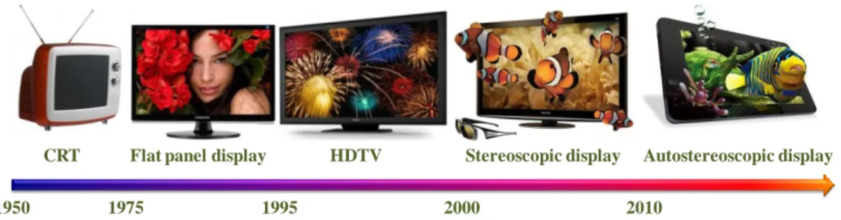
Fig. 1- 1 History of display technology
CRT Flat panel display HDTV Stereoscopic display Autostereoscopic display 1950 1975 1995 2000 2010
2
1.2 Principles of 3D image
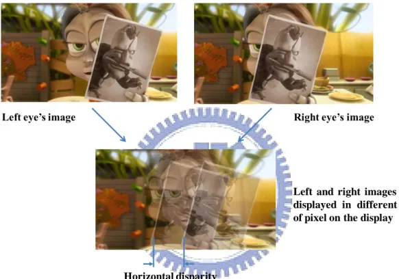
Binocular vision allows humans to get the depth information that results from our two forward-facing eyes, called stereopsis [1][2]. There is a slightly different viewpoint perceived by each eye, and our brain will calculate this disparity as the sensation of depth [Fig. 1-2].
Fig. 1- 2 Horizontal disparity
Horizontal disparity
Left eye’s image Right eye’s image
Left and right images are displayed in different set of pixel on the display
3
With monocular vision [3], people can also perceive the depth of the real world by experiences and time learning. For example, the depth sensation of a picture can be felt by shading, interposition, linear perspective and so on, as shown in Fig 1-3.
Fig. 1- 3 Picture illustrating depth cues
Moreover, oculomotor depth can be categorized into vergence and accommodation [4] due to feedback from our eyes’ muscles. The vergence is defined as the angle of the viewing target to our eyes [Fig. 1-4]. The accommodation is the crystalline lens focus on an object to get a clear image, as shown in Fig. 1-5. Both of these are generally regarded to help judging the depth information.
Fig. 1- 4 Vergence angle Interposition Texture Gradient Aerial distortion Shading Linear perspective
40 °
10 °
4
Fig. 1- 5 Accommodation
It is also necessary to imitate the binocular system allowing viewers’ left and right eye to each perceive its own image and form a 3D image in order to apply 3D images on flat panel displays.
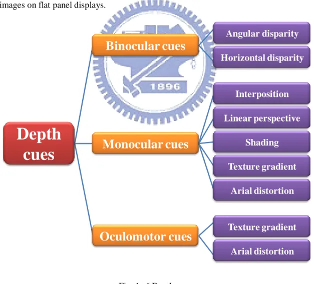
Fig. 1- 6 Depth cues
Binocular cues
Oculomotor cues
Monocular cues
Angular disparity Horizontal disparity Interposition Linear perspective Shading Texture gradient Arial distortion Texture gradient Arial distortionDepth
cues
5
1.3 3D display technologies
Nowadays, 3D display technology has been briefly classified in two parts. One is stereoscopic which needs extra devices; the other is auto-stereoscopic which is without extra devices, as shown in Fig. 1-7. The details of two types are described following.
Fig. 1- 7 Classification of 3D display technology
1.3.1 Stereoscopic displays
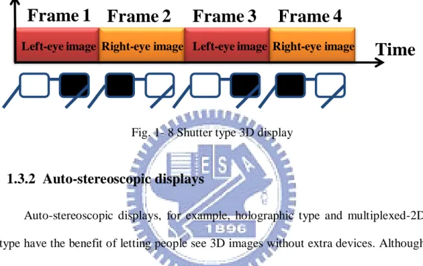
Stereoscopic display requires viewers to wear a device such as glasses, or a helmet to see the 3D image [5][6]. The main purpose is to ensure images are seen correctly by the left and right eye respectively. For example, the shutter type, the display shows a left eye image in the first frame and the left glass will be transparent at the same time, while the right glass is blocked; on the contrary, in the second frame, the display shows a right image and the right glass will be transparent [Fig. 1-8].
Stereoscopic (with glasses) Auto-stereoscopic (without glasses) Shutter Polarization Spatial-Multiplexed Time-Multiplexed
3D display
technology
Anaglyph HMD Holography Volumetric Multi-plane Multiplexed-2D6
The display is synchronized with the shutter glasses. One glass will be shuttered when the other is transparent. Therefore, our left and right eye receives different images and our brain then combines them into a 3D image. No matter what kind of stereoscopic display, the common issue is that the extra-devices are uncomfortable and inconvenient to wear.
Fig. 1- 8 Shutter type 3D display
1.3.2 Auto-stereoscopic displays
Auto-stereoscopic displays, for example, holographic type and multiplexed-2D type have the benefit of letting people see 3D images without extra devices. Although the holographic type can show a realistic 3D image, it is hard to fabricate on a large scale screen. Multiplexed-2D type has the advantage of its thin scale. Moreover, the multiplexed-2D type can easily be implemented with flat panel displays which are widely used today. As the result, many researches are interested in these aspects. Following, we also simply divide multiplexed-2D type into time-multiplexed and spatial-multiplexed for describing clearly.
Time
Right-eye imageFrame 1
Left-eye image Left-eye image Right-eye image
7
1.3.3 Multiplexed 2D type displays
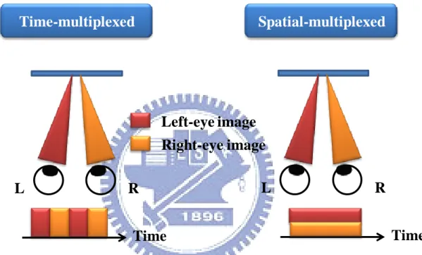
The general concept of time-multiplexed and spatial-multiplexed is projecting different images to both eyes individually, as shown in Fig. 1-9. The time-multiplexed type with high resolution per view needs high speed display elements to project to left and right eyes sequentially [7][8][9]. The spatially multiplexed type provides left and right images at the same time nevertheless the lower resolution per view is caused.
Fig. 1- 9 Concept of the time and spatial multiplexed type
These time-multiplexed systems has many kind of configurations been proposed. For example, one uses a micro-optic structure on the principle of total internal reflection (TIR) that makes the light go through the desired direction, as shown in Fig. 1-10 [10]. Thus the 3D image can be observed by switching the two light sources sequentially.
Time-multiplexed
Spatial-multiplexed
Time
R
L
Time
R
L
Left-eye image
Right-eye image
8
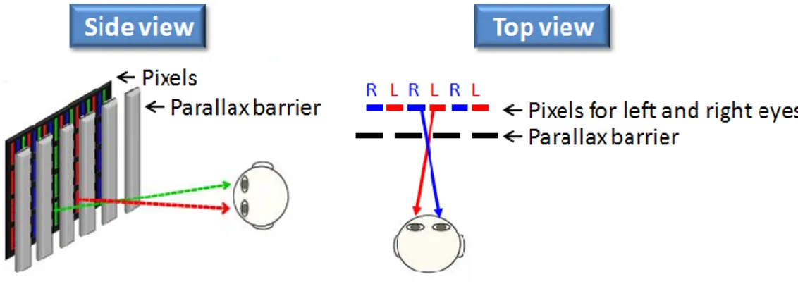
Fig. 1- 10 3D display based on sequentially switching backlight with focusing foil There also are some configurations for spatial-multiplexed type such as parallax barrier [11][12] and lenticular lens array [13][14], and have been widely used in 3D flat panel display. These optical components are used to project the images to left and right eye-viewing windows at the desired viewing position. Both of them are briefly introduced in the following section.
Parallax barrier
Parallax barrier blocks the light by using strips of black mask. Its optical design adjusts the viewing angles and position by optimizing barrier’s geometry, as shown in Fig 1-11. The parallax barrier is perhaps the simplest way to do this work, however, the main disadvantage is that opaque areas will reduce the brightness of display.
Fig. 1- 11 Spatial multiplexed displays: parallax barrier
θ
α
Lightguide
LCD
9
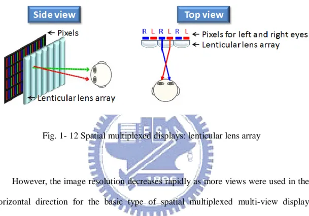
Lenticular lens array
Lenticular lens array are typically cylindrical lenses arranged vertically with respect to a display. The cylindrical lenses direct the light from a pixel to the design angle in front of the display, as shown in Fig 1-12. For the transparent lens, the brightness can still be kept.
Fig. 1- 12 Spatial multiplexed displays: lenticular lens array
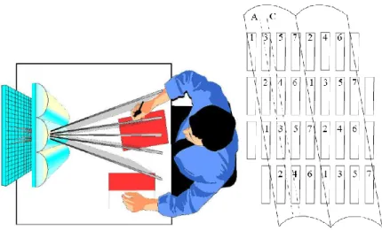
However, the image resolution decreases rapidly as more views were used in the horizontal direction for the basic type of spatial multiplexed multi-view display although it much easy to be implemented. Therefore, the company, Philips, proposed a slanted lenticular lens array [15][16] to share the resolution reduction between horizontal and vertical direction, as shown in Fig 1-13 to overcome this drawback,. Because the resolution has been decreased in this method, and there is no need to show 3D images all the time. Thus, the 2D/3D switchable display is sure to carry out.
10
Fig. 1- 13 Slanted lenticular lens 3D display with multi-view by the Philips Company
1.3.4 2D/3D switching methods
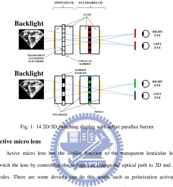
The 2D/3D switchable displays provide more functions and options to users. For example, users may watch an exciting video in 3D mode and read an interesting article switching to 2D mode. In these years, there are several techniques can switch the images between 2D and 3D, and briefly be divided into active parallax barriers [17], activated micro lens [18][19][20][21].
Active parallax barrier
The active parallax barrier is able to block the light as turn on voltage to form the barrier. Thus the 3D images can be obtained. N the other hand, , the parallax barrier become totally transparent and let all light pass through it to form 2D images when turning off the voltage. The same as mentioned before, the opaque areas still reduce the brightness of display in 3D mode.
11
Fig. 1- 14 2D/3D switching display with active parallax barrier
Active micro lens
Active micro lens has the similar function to the transparent lenticular lens. Switch the lens by controlling the voltage can change the optical path to 2D and 3D modes. There are some devices can do this work, such as polarization activated micro-lens [22], active LC lenticular lens [23], and electric-field driven LC lens (ELC lens), are illustrated following.
1. Polarization activated micro-lens:
The polarization switching cell can change the polarization state likes the conventional LCD panel. And then the polarized light passes through the LC type GRIN lens, as shown in Fig 1-15. At the homogeneous state, the polarized light passes through the LC with the same refractive index of the glass. On the other hand, the changed-polarized light passes through the LC with different refractive index of the glass when applying a voltage on polarization switching cell. Thus, the inhomogeneous state will cause the refraction and will converge the light.
RIGHT EYE LEFT EYE BACKLIGHT RIGHT EYE LEFT EYE BACKLIGHT SWITCH LCD STANDARD LCD GLASS PIXELS TRANSPARENT PATTERNED ELECTRODE POLARIZER BARRIER ENABLED PARALLAX BARRIER
Backlight
Backlight
12
Fig. 1- 15 Polarization activated micro-lens 2. Active LC lenticular lens:
The polarized light has been converged by the different refractive index between LC and the glasses. The liquid crystal will change its direction and cause the LC refractive index to be same with the glass as applying a voltage on the LC lens. However, the mismatching around the interface between concave structure and LC molecules is hard to achieve a complete lens off state.
Fig. 1- 16 Active LC lenticular lens
~
~
Pixels Polarization Switch LC type GRIN lens (a) (b)~
~
Pixels LC Concave lens (a) (b)13 3. Electric-field-driven LC lens (ELC lens):
The most attractive characteristic of ELC lens is its simple structure and easy fabrication. The ITO placed out of the top glass substrate would make the electric field distribution much smoother, but cause the high operating voltage. The bottom substrate was coated with ITO on the whole surface. As applying voltage on the top electrodes, the LC cell will become to a GRIN lens.
Fig. 1- 17 Electric-field-driven LC lens (ELC lens) 4. Multi-electrode driven liquid crystal lens (MeD-LC Lens)
The concept of MeD-LC lens is similar to ELC lens, as shown in Fig. 1-18. At the voltage off state, incident light passes through the MeD-LC lens cell without change of propagation direction. The electric field at the lens edge is stronger than at the lens center for applying certain voltage on different electrodes. Therefore, a non-uniform angle of LC director and the refractive index causes a phase difference and changes light direction.
~
~
Pixels LC
14
Fig. 1- 18 Principle of the MeD-LC lens
The principle of liquid crystal lens and driving method will introduce in the next sections.
1.4 Introduction to liquid crystal
Liquid crystal has an orientational order as the most important feature that makes anisotropic physical property such as an electric field, a magnetic field. For the rod-like molecules, the average directions of long molecule axes in nematic phase are along a common direction by the unit vector , as shown in Fig. 1-19.
Fig. 1- 19 Schematic diagram showing the orientation of rod-like molecules
~
~
Pixels LC (a) (b) 2D mode 3D mode n15
Because the permittivity in the direction parallel to is different that from the direction perpendicular to , the induced polarization depends on the orientation of the liquid crystal director with the respect to the applied field. The electric energy of liquid crystal per unit volume is approximately given by
(1-1) If the liquid crystal has a positive dielectric anisotropy ( ), the electric energy is minimized when liquid crystal director is parallel to the applied field ( ). Conversely, if the liquid crystal has a negative dielectric anisotropy ( ), then the liquid crystal director tends to perpendicular to the applied field to minimized the electric energy [24].
Thus, the LC orientation will be changed by the electric energy, and the refractive index can be controlled by the applied voltage.
Fig. 1- 20 Geometry to calculate refractive index change with liquid crystal molecule orientation
In uniaxial crystals the index ellipsoid can be shown in Fig 1-20. The first mode, called the ordinary wave, has a refractive index no regardless of . In accordance
X Z Xθ Zθ nθ ne no θ
16
with the ellipse shown in Fig 1-20, the second mode, called extraordinary wave, has a refractive index that varies from no when =0, to ne when =90. When the direction
of liquid crystal is not rotated, the light will be affected by the refractive index ne.
when the liquid crystal axis is rotate with an angle , the light will be affected by no
and ne.
This slice of the indicatrix can be expressed as Eq. 1-2.
(1-2) And
(1-3) Therefore, Eq.1-1 can be written as Eq.1-3.
(1-4) Equivalently, (1-5)
Thus, the equivalence equation of rotate angle can be derived as Eq.1-6.
(1-6) Since the nematic liquid crystal does not align uniformly across the cell in the thickness direction, a more useful form to solve the as Eq.1-7.
(1-7)
This formula indicates the relation between effective refractive index and angular orientation of the namatic liquid crystal.
17
1.5 Liquid crystal lens (LC lens)
The LC lens [25][26] has the same focus effect as the conventional optical lens. Fig 1-21 shows how the conventional lens focuses the light. As a plane wave incident light passes through a lens, the wave fronts converge to a focal point due to the optical path difference (OPD). The OPD can be defined as (where n is refractive index and d is the path length).
Fig. 1- 21 Conventional lens
A graded–index (GRIN) material [27] has a refractive index that varies continuously with position, n(r). The OPD can be defined as . The relation between refractive index and position has been shown in Fig. 1-22. The refractive index increases from the outer to the center.
Fig. 1- 22 GRIN lens
f
Focal length
z
r
18
As we assume that the focal point is larger than the incident position (f>r) and the refractive of the center is large than the edge ( n(0) > n(r) ). The light velocity is
inverse proportional to the refractive index as formula shows. Therefore, the wave fronts will slow down in the dense region and speed up in the rare region and causing the light to focus.
Fig. 1- 23 The geometry of the focused GRIN Lens
A ray traverses the lens on the optical axis passes along the optical path length (OPL) as . For a ray traverses at a height , overlooking the slight bending of ray path, . Since a planer wave front must be bent into spherical wave fronts, the OPLs from one to the other, along any route must be equal as followed,
(1-8) And (1-9) By substitution, (1-10)
n
2
n
1
n
(r)
r
d
R
F
19
Where is the refractive index difference between center and the edge ( ), if can be neglected, the focusing formula results in Eq.1-11.
(1-11) By substitution,
(1-12) Where can be written as a parabolic function with a constant ,
(1-13) According to the formula 1-13 derived above, the GRIN lens will focus at point f when the distribution of refractive index is closed to a parabolic function. The GRIN lens and conventional lens are both the fixed focal lens. Thus, the LC lens is proposed to be a tunable focus lens with variable focal length.
Focal length of a LC lens is defined in Eq. 1-11. The liquid crystal direction can be controlled by the applying voltage. When light passes through the LC layer, the continuous-changing refractive index causes the phase retardation to act as a lens.
Fig. 1- 24 LC cylindrical lens
Rubbing direction Electrode (ITO) LC layer Electrode Glass Glass d
20
(a) (b) Fig. 1- 25 (a) Lens off (b) Lens on
1.6 LC lens with 2D/3D switching
The catalogue of 2D/3D LC lens switching methods as mentioned before is shown in Table. 1-1. Generally speaking, these LC lens have some advantages and also have some disadvantages. Active LC lenticular lens and polarization active micro-lens have an issue of complex fabrication. ELC lens and MeD-LC lens have much simpler fabrication; however, the long switching time between 2D and 3D is about 4~10 sec depending on the LC cell gap.
Glass ITO LC layer Glass ITO V1 V0 V1>V0=0 volt E-field
21
Table. 1- 1 2D/3D LC lens switching methods
1.7 Motivation and objective
People have been surrounded by displays more and more often in these days. 3D displays are much more realistic and may replace 2D displays as the next mainstream in the market. However, 3D displays still need to overcome some issues. The parallex barrier has lower brightness than lenticular lens. Both of parallex barrier and lenticular lens will loss more resolution as showing more views. Consequently, active optical 2D/3D switching devices are surely needed.
According to Table 1-1, the electrode type LC lens is a better choice for its simple fabrication. The High Resistance TFT Liquid Crystal Lens (HR-TFT LC lens) was combining high-resistance layer with TFTs structure. The high-resistance layer coating between the ITO electrodes created the continuous electric field. The TFTs is an on/off switch. The resistance value is corresponding to the applying gate voltage.
~ ~
~
22
HR-TFT LC lens has high resistance layer characteristic when the gate turns off. And it will be the TFTs letting current pass through the coating layer as the gate turns on. Therefore, the HR-TFT LC lens has multifunction such as, 2D/3D switchable, 2D/3D rotatable, 2D/3D localized. In this thesis, the 2D/3D localized function was proposed.
Fig. 1- 26 Sketch of high-resistance TFT liquid crystal lens
1.8 Organization
This thesis is organized as following: the fabrication process of the HR-TFT LC lens will be introduced in detail in Chapter 2. In Chapter 3, the design and simulation result of the HR-TFT LC lens and discussion will be presented. Additionally, this chapter also shows the driving method of the HR-TFT LC lens. The experimental result and summary will be shown in Chapter 4. Finally, the conclusions and future work of this thesis will be discussed inChapter 5.
Glass LC layer Gate ITO a-IGZO ITO Glass SiO2 Source/Drain ITO
23
Chapter 2
Fabrication and Measurement System
2.1 Introduction
The fabrication of HR-TFT LC lens is described in this chapter. The thickness of substrate glass is 550 . Firstly, the glass substrate is cleaned by the standard process. Secondly, the semiconductor process including spin coating, lithography, sputtering, PECVD and leave-off is utilized in order to obtain the desired pattern. Thirdly, high-resistance layer is coated by the sputter and annealed by the furnace. Fourthly, the alignment layer is made by the spin coating and rubbing techniques. Fifthly, the top and bottom glass is assembled by ball spacers 30 to control the cell gap, and then filed in LC (E7). Finally, wires for various voltage driving will connect to each electrode.
2.2 Fabrication processes
This section describes the cell fabrication process including spin coating, lithography, wet etching, sputtering, annealing, rubbing, assembling. The detail process steps were listed below and as shown in Fig. 2-1.
24
Fig. 2- 1 Fabrication steps
Glass cleaning Patterned glass cleaning Patterned glass cleaning IGZO sputtering Lithography OM checking ITO wet etching
PECVD Lithography OM checking ITO sputtering PI coating Rubbing Assembling Soldering ITO patterning (Gate) Insulator (SiO2) & ITO patterning (Source/Drain) LC alignment layer & Assembling Annealing
25
I. Glass cleaning
For the transparent characteristic, glass has been widely used as the substrate for the display. In the fabrication, the glass of 0.55 mm thick is chosen and coated with ITO thin film already. The detailed sequence is as follow:
Step 1 : Place the glasses on the Teflon carrier, and put into a container with acetone as shown in Fig. 2-2. Ultrasonic vibrate for 20 minutes to remove the organic contamination on the glasses.
Step 2 : Rinse the glasses by DI water for 1 minute. Step 3 : Rubbing the glasses with detergent by hands. Step 4 : Rinse the glasses by DI water for 1 minute.
Step 5 : Place the glasses on the Teflon carrier, and put into a container with DI water as shown in Fig. 2-2. Ultrasonic vibrate for 40 minutes to remove the remained particle and detergent on the glass.
Step 6 : Use N2 purge to dry the glasses, and place glasses into a glass container with
a cover.
Step 7 : Put the glass container into an oven with 110℃ for 30 minutes.
26
II. ITO pattering and insulator
The gate ITO pattering detailed sequence is as follow and also can refer to Fig. 2-4. Step 1: Before the lithography process, glass substrate was cleaned by step I.
Step 2: Put the glasses on the metal holder and put into the HMDS oven to eliminate the surplus steam and improve the adhesion between organic photoresist and the ITO film.
Step 3: A positive photoresist was applied and coated on the ITO film.
Step 4: Soft bake for one and a half minutes, to eliminate most of the solvent of the photoresist and enhance the adhesion.
Step 5: Expose the glass with ultra-violet (UV) light source through shadow mask for 40 seconds. Consequently, the pattern on the mask was transformed to the positive photoresist after developing. The mask is shown in Fig. 2-3.
Step 6: Check the pattern by optical microscope (OM), to see if there is any broken line, and the hard bake for three minutes.
Step 7: Use wet etching technique and remove the photoresist, and the desired ITO pattern can be reserved.
Fig. 2- 3 The mask pattern of gate substrate and bottom lock
75um 12um
40um
27
Fig. 2- 4 Flow of fabricating gate ITO electrode (a) glass substrate with ITO film,
(b) spin-coating positive photoresist upon the glass substrate, (c) using lithography technique to obtain the latent image, (d) using leave-off technique to remove photoresist and reserve
the desired ITO pattern
ITO
Glass substrate
Photoresist
Photoresist
ITO
ITO (Gate)
(a)
(b)
(c)
(d)
28
The insulator and source/drain ITO pattering detailed is as follow and refer to Fig. 2-6.
Step 1: Use PECVD (Plasma-enhanced chemical vapor deposition) to produce 300nm thick SiO2 insulator.
Step 2: Put the glasses on the metal holder and put into the HMDS oven to eliminate the surplus steam and improve the adhesion between photoresist and ITO. Step 3: A positive photoresist was applied and coated on the insulator.
Step 4: Soft bake for one and a half minutes, to eliminate most of the solvent of the photoresist and enhance the adhesion.
Step 5: Expose the glass with ultra-violet (UV) light source through shadow mask for 40 seconds. Consequently, the pattern on the mask was transformed to the positive photoresist after developing. The mask is shown in Fig. 2-5.
Step 6: Check the pattern by optical microscope (OM), to see if there is any broken line, and the hard bake for three minutes.
Step 7: Sputter ITO upon the patterned photoresist.
Step 8: remove the photoresist, and the desired ITO pattern can be reserved.
Step 9: RIE (Reactive-ion etching) process is used to remove the insulator where cover on the gate ITO soldered area. The pattern is shown in Fig. 2-7.
Fig. 2- 5 The mask pattern of source/drain substrate and top lock
72.5um 14.5um 20um 30um 30um 30um 10um 10um 30um 20um 10um 10um
29
Fig. 2- 6 Flow of fabricating insulator and source/drain ITO electrode (a) SiO2 insulator on gate substrate,
(b) spin-coating positive photoresist upon the glass substrate, (c) using lithography technique to obtain the latent image, (d) sputtering ITO,
(e) using leave-off technique to remove photoresist and reserve the desired ITO pattern
ITO
SiO
2Photoresist
Photoresist
SiO
2ITO
ITO (Source/Drain)
SiO
2( Insulator)
(a)
(b)
(c)
(d)
(e)
30
Fig. 2- 7 The pattern after RIE and the lock
III. High-resistance layer and annealing
The high-resistance layer after sputtering a-IGZO can refer to Fig. 2-8. The high vacuum sputter system in NCTU with background pressure about 3×10⁻⁶ torr was placed in class 14K clean room. Vacuum system composes of rotary pump and cryo pump, which work for different pressure range. Power system consists of several DC and RF power modules with 6 sputtering guns and the purified gas sources of argon, nitrogen, and oxygen gas. The substrate planetary rotation system can bring uniformity by rotating the sample disk and holders.
Fig. 2- 8 High-resistance a-IGZO on the substrate
RIE
100um
100um
IGZO (Active layer) SiO2( Insulator)
31
The a-IGZO active layer with 80nm in thick was deposited upon the substrate we made sputtering with an In2GaZnO5 target at room temperature. The deposition was
done at DC power = 100W without any intentional substrate heating, working pressure =3mtorr and argon flow rate = 10sccm [28].
Finally, the device was annealed in nitrogen ambience at 350℃ for an hour by atmospheric anneal furnace to rearrange the a-IGZO lattice again. After annealing process, the electrical characteristics of the device are better than the device without annealing.
32
IV. LC alignment layer and assembling
Step 1: Cleaning the patterned glass with step I.
Step 3: Coating the solvent to make the PI adhesion more efficiently. Step 4: Coating the PI.
Step 5: Put the glasses into an oven with 220℃ for 60 minutes.
Step 6: Rubbing the glasses with parallel to the ITO pattern and make the rubbing direction mark.
Step 7: Paste two line spacers (30μm) on two sides of bottom glass and apply UV glue on the spacers.
Step 8: Make sure the top and bottom electrode overlap to each other. Then, put the bottom glass on the top glass and fixed with a tape.
Step 9: Press on both top and bottom glasses to make sure the cell gap identically. Step 10: Fill in the LC after curing.
Step 11: Seal the edge with UV glue and curing.
The ultrasonic solder was soldered on the electrode to enhance the adhesive of the solder and smeared with AB glue to avoid the wires coming off. Finally, the High-resistance TFT Liquid Crystal Lens (HR-TFT LC lens) will be measured.
Fig. 2- 9 Prototype of HR-TFT LC lens
75um
33
2.3 Measurement system
I. CCD system
After the fabrication process, the optical properties of the HR-TFT LC lens are measured by CCD. And the experiment setup is shown in Fig. 2-10. At first, the polarizer was set to be parallel to the rubbing direction of alignment layer. The LC direction was controlled by the voltage and the HR-TFT LC lens was able to act as a GRIN lens and focused at a certain point. By placing CCD at the focal point of the HR-TFT LC lens, the intensity image and beam size of the HR-TFT LC lens could be measured.
Fig. 2- 10 Experimental setup
II. Electrical characteristics
The device electrical properties and transfer characteristics for a-IGZO TFTs are measured by a semiconductor parameter analyzer (Keithley 4200) in the dark at room temperature. In the transfer characteristic (IGS-VDS), the VDS are conventionally swept
from -10 to 30V at the step VGS (step = 0.5V) to measure the corresponding IDS.
In our experiment, the HR-TFT LC lens is measured by these two methods, and the results will be given in Chapter 4.
Beam Expander CCD Polarizer Analyzer He-Ne Laser (633nm) LC lens Pinhole
Optical bread board
34
2.4 Summary
During the fabrication processes, there are many factors which would affect the quality of HR-TFT LC lens. The a-IGZO layer as our high-resistance layer will affect the electric field distribution and the LC lens performance. Therefore, we would like to obtain a desired electrical property and high resistance value for a quality LC lens. After the fabrication, we used the CCD to measure the optical properties and electric properties.
35
Chapter 3
Principle of High Resistance TFT Liquid
Crystal Lens (HR-TFT LC lens)
The structure design and simulation results of HR-TFT LC lens are described in this chapter. Firstly, the two main functions of the proposed HR-TFT LC lens: the high resistance layer for building a high quality LC lens, and the active TFT structure for locally switching are introduced. Secondly, the simulation and experimental results are clarified. Finally the operating process of HR-TFT LC lens is illustrated.
3.1 Introduction of HR-TFT LC lens
The electrode type LC lens for its simple fabrication is a better choice to develop. The HR-TFT LC lens has been proposed to obtain 2D/3D localized LC lens. The HR-TFT LC lens can be divided into two parts.
Y. P. Huang et al.[30], proposed a Multi-electrode Driven LC (MeD-LC) lens which placed the controlled electrodes out of the glass substrate to be a high-K material layer. Therefore, a smooth electric field distribution that also means a parabolic refractive index distribution of the LC lens can be obtained. However, the operating voltage of the MeD-LC lens is high (about 30Vrms). So, the best way to reduce the driving voltage is placing the controlled electrodes into the cell although the discrete electric field is occurred. Consequently, in this thesis the high resistance layer is used to replace the multi electrode structure of the LC lens to overcome the discontinuous electric field issue. The high resistance layer coated on the electrodes can be seemed as a group of fine electrodes that a high to low gradient voltage
36
distribution on the high resistance layer can be generated [Fig. 3-1]. In a brief summary, the proposed high-resistance liquid crystal lens (HR-LC lens) lens has two benefits: low driving voltage and simple driving circuit. It is believed that the HR-LC lens is more suitable for showing 3D images and easier for implementing in real product [31][32].
In this paper we used the transparent semiconductor material, IGZO, to be the high resistance layer. The IGZO material is wide used to be the active layer for TFT devices [33][34]. Therefore, in this paper we further extend the previous HR-LC lens and propose a novel LC device: a transparent IGZO-TFT is addressed on the LC Lens as shown in Fig. 3-1. Similar to the general TFT operating mechanism, the current can easily pass through the low resistance layer when the resistance value is as low as the conductor during gate-on state. It also means the ITO pattern electrodes and high resistance layer will approach a planar electrode at that time. And the side electrodes are played as the drain electrode to charge to the middle electrodes (source electrode). When gate voltage is off, the resistance layer changes back to a high resistance material. Thus, a small leakage current just can pass through it.
Based on the high-resistance layer and TFTs functions, the 2D/3D localized could be obtained by the HR-TFT LC lens. To our best knowledge, this is the first report that an active HR-TFT LC lens is proposed.
37
Fig. 3- 1 Structure of HR-TFT LC lens
Table. 3- 1 Parameters of HR-TFT LC lens
Glass
LC layer
Gate ITO
a-IGZO
ITO
Glass
SiO
2Source/Drain
ITO
R
ch
R
ch
Rubbing direction ITO (Gate ) SiO2(insulator) ITO (S/D) HR layer LC layer ITO Glass GlassHR-TFT LC lens
Value
Lens pitch
188.5 um
Electrode width
14.5 um
Slit width
72.5 um
Cell gap
30 um
LC material
E7(Δn=0.22)
Focal length
0.67 mm
38
3.2 Simulation and comparison to traditional LC lens
In this section the LC director profile and electric field distribution of traditional LC lens and our HR-TFT LC lens were calculated and compared by the commercial software 2D-MOS, as shown in Fig. 3-2. When applying a high operating voltage to the electrodes of the traditional LC lens, the electric field could not affect the LC under the non-slit area well [Fig. 3-2(a)]. Thus, its refractive index distribution was very different from the parabolic curve, i.e. a low quality LC lens; on the contrary, for the HR-TFT LC lens, the LC under the non-slit area could be affected because the resistance layer had a voltage distribution on it [Fig. 3-2(b)]. As the result, the refractive index distribution of proposed HR-TFT LC lens effectively provided a gradient electric field distribution which was closer to the ideal parabolic curve than the traditional one. The refractive index distribution of HR-TFT lens and traditional LC lens were obtained and shown in Fig. 3-3. In a brief summary, the high resistance layer could provide smoother electric field distribution within the cell, that the high quality LC lens could be obtained.
39 (a)
(b)
Fig. 3- 2 The LC director profile and electric field distribution by simulation software 2D-MOS of (a) traditional LC lens (b) HR-TFT LC lens
ITO
Glass
ITO
Glass
V
highV
lowV
highLC layer
ITO
Glass
V
highV
lowHigh-R
layer
LC layer
V
highITO
Glass
SiO
240 1.5 1.55 1.6 1.65 1.7 1.75 1.8 -0.1 -0.05 0 0.05 0.1 數列2 數列1 1.5 1.55 1.6 1.65 1.7 1.75 1.8 -0.1 -0.05 0 0.05 0.1 數列2 數列1 1.5 1.55 1.6 1.65 1.7 1.75 1.8 -0.1 -0.05 0 0.05 0.1 數列2 數列1
Ideal LC lens
Traditional LC lens
HR-TFT LC lens
(a) (b)Fig. 3- 3 Simulation results of refraction index distribution of ideal LC lens, traditional LC lens, HR-TFT LC lens
3.3 Operation of HR-TFT LC lens
The operating process of HR-TFT LC lens is described in this section. In the lens-off state, the all electrodes are kept in 0 volt for the 2D mode [Fig. 3-4(a)]. While the lens for the localized 3D mode, one voltage will be applied on source electrodes; meanwhile, another voltage will applied on gate electrodes to lower the resistance value and turn the TFTs on. Therefore, the drain electrodes are charged by the source electrodes [Fig. 3-4(b)]. From there, the gate voltage and the source voltage are switched to 0 volt and turn the TFTs off to hold on the lens on state. Therefore, the LC
n
r(mm)
1.8 1.71.6
1.5
-0.1
0
0.1
n
r(mm)
1.8 1.71.6
1.5
-0.1
0
0.1
41
lens is hold on the drain electrodes until the next charging state [Fig. 3-4(c)].
(a)
(b)
(c)
Fig. 3- 4 Operating process of HR-TFT LC lens (a) initial state (b) charging state (c) holding state
Drain ITO Glass LC layer Gate ITO a-IGZO ITO Glass SiO2 Source ITO Drain ITO ITO Glass LC layer a-IGZO Glass SiO2 Gate ITO Source ITO Drain ITO ITO Glass LC layer a-IGZO Glass SiO2 Gate ITO Source ITO
42
Fig. 3- 5 Lens array of HR-TFT LC lens
3.4 Summary
The proposed HR-TFT LC lens has benefits such as low driving voltage, simple driving circuit, and good focus ability. Furthermore, switching the gate electrode on or off, the high resistance layer can be modulated that an active switching HR-TFT LC lens is obtained. Accordingly, the first proposed HR-TFT LC lens can be used on for some advanced applications such as locally 2D/3D switching auto-stereoscopic displays.
The experimental results will be discussed in the next chapter.
Gate ITO Source ITO Drain ITO LC layer a-IGZO SiO2 Glass LC layer Gate ITO a-IGZO ITO Glass SiO2 Source ITO Drain ITO
43
Chapter 4
Measurement Results
4.1 Introduction
The objective of measurement is to investigate the lens performance, transmittance, electrical characteristics and holding time of HR-TFT LC lens. According to the simulation results in Chapter 3, the experiments in this chapter would confirm our concepts.
4.2 Measurement results
The prototype with two HR-TFT LC lenses was fabricated as shown in Fig. 4-1. The top substrate has 4 gate electrodes and 5 source/drain electrodes. These individual electrodes can be controlled by different operating voltages to form a lens shape. After fabrication, the HR-TFT LC lens was measured in four parts: equivalent LC lens shape, transmittance, electrical characteristics and holding time.
Fig. 4- 1 HR-TFT LC lens prototype
Top glass LC layer Gate ITO Drain ITO Source ITO Bottom glass
Top view
Side view
44
4.2.1 Reconstruction of the HR-TFT LC lens
From the experimental setup as mentioned in 2.3, the fringing pattern can be captured by CCD. The fringing pattern (Fig. 4-2) is utilized to observe the phase retardation of the LC lens. According to the fringing pattern, these bright and dark series lines can reconstruct Δ n profile and estimate the optical property. The refractive index distribution of proposed HR-TFT LC lens effectively provides a gradient electric field distribution. The resistance is about 3MΩ/□, as measured the data between source and drain electrodes. The result of refractive index distribution of HR-TFT LC lens is closed to the ideal parabolic curve as shown in Fig.4-3.
Fig. 4- 2 HR-TFT LC lens fringing pattern
45
4.2.2 Transmittance of the HR-TFT LC lens
The brightness is always a critical parameter for a display. Thus a high transparent HR-TFT LC lens placed in front the display is needed. We fabricated a multi-layer HR-TFT LC lens, and the measurement is shown in Fig. 4-4. Fig. 4-4 shows that the transmittance of the HR-TFT LC lens is above 90% in the visible wavelength. For the a-IGZO absorbs the ultraviolet, the transmittance decreases in the UV wavelength.
Fig. 4- 4 HR-TFT LC lens refractive index distribution
4.2.3 Analysis of the electrical properties
The transfer characteristic of a-IGZO TFTs for inverted-coplanar structure is shown in Fig. 4-5. Fig. 4-5(a) shows the a-IGZO TFTs annealing at 400℃ exhibit a Vth of 6.6 (V), a S value of 0.8179 (V/decade), a μ FE of 6.52 (cm2/Vs), and a Ion/Ioff
of 7E5; Similiarly, Fig. 4-5(b) shows the a-IGZO TFTs annealing at 350℃ exhibit a Vth of 5.0 (V), a S value of 0.7122 (V/decade), a μ FE of 9.03 (cm2/Vs), and a Ion/Ioff
of 1.2E6. All of the parameters are summarized in Tab. 4-1. The comparison between
70 75 80 85 90 95 100 105 300 400 500 600 700 800 T ra n sm it ta n ce (% ) Wavelength(nm) 70 75 80 85 90 95 100 105 300 400 500 600 700 800 T ran sm it tan ce (% ) Wavelength(nm) ITO ITO+SiO2_2800Å ITO+SiO2+ITO ITO+SiO2+ITO+IGZO(40nm) ITO+SiO2+ITO+IGZO(80nm)
46
these two annealing temperatures shows 350℃ has a better electrical properties, such as the lower Vth (i.e. the lower power consumption cost), larger current (i.e. the better
charge property), and higher mobility.
(a)
(b)
Fig. 4- 5 a-IGZO TFTs transfer characteristics (a) 400℃ annealing (b) 350℃ annealing
Table. 4- 1 Electrical parameters of a-IGZO TFTs
1.0E-12 1.0E-11 1.0E-10 1.0E-09 1.0E-08 1.0E-07 1.0E-06 1.0E-05 1.0E-04 -15 -10 -5 0 5 10 15 20 25 30 35 1E-4 1E-5 1E-6 1E-7 1E-8 1E-9 1E-10 1E-11 1E-12 -15 -10 -5 0 5 10 15 20 25 30 35
400
℃
V
DS=5.0
1.0E-12 1.0E-11 1.0E-10 1.0E-09 1.0E-08 1.0E-07 1.0E-06 1.0E-05 1.0E-04 -15 -10 -5 0 5 10 15 20 25 30 35 1E-4 1E-5 1E-6 1E-7 1E-8 1E-9 1E-10 1E-11 1E-12 -15 -10 -5 0 5 10 15 20 25 30 35350
℃
V
DS=5.0
Temperture
(℃)
V
th(V)
S value
(V/decade)
u
FE(cm
2/Vs)
I
on/I
off400
6.6
0.8179
6.52
7.0E5
350
5
0.7122
9.03
1.2E6
47
Fig. 4- 6 a-IGZO TFT structure
Moreover, the definitions of each parameter in the TFT part are following:
Vth (Threshold voltage): the value of VGS at which a sufficient number of mobile
electrons accumulate in the channel region to form a conducting channel.
S (Subthreshold swing): S, defined as the voltage required increasing the drain
current by a factor of 10, is given by
(Field effect mobility): the mobility is an important parameter of the
semiconductor since it describes how fast a particle can move due to an electric field. The is defined by the transconductance (gm) at a low drain voltage (VDS=0.1V).
Derived from the transfer characteristic in Eq. 4-1, when VD is much smaller than
VG – Vth or VG > Vth, the drain current can be approximated as Eq. 4-2.
(4-1) When VG – Vth or VG > Vth , (4-2) Transconductance is defined as (4-3) L=72.5um Insulator W=1.5cm
Vs
Vd
Vg
Semiconductor48 Thus, is obtained from Eq. 4-3:
(4-4)
Ion/Ioff (drain-current ratio): on-current (Ion) determines the rate of the charging and
the off-current (Ioff) is associated with the leakage of the voltage.
4.2.4 Holding time of HR-TFT LC lens
The equivalent electric circuit of the HR-TFT LC lens and the voltage output are shown in Fig. 4-7. CLC is about 3.98pF after calculating (
). For the electric potential saving on the drain electrodes, a 5uF storage capacitor is added parallel connection to the CLC [Fig. 4-7 (a)]. The
storage capacitor can reduce the electric potential various which is caused by the leakage current. Therefore, the electric potential can be effectively saved on the drain electrodes. The source voltage operates at ±5 voltages 60Hz, and the gate voltage operates at 0~30 voltages 120Hz pulse function.
(a) (b)
Fig. 4- 7 HR-TFT LC lens (a) electric circuit (b) voltage output signal
CLC Vg Vd Vs Cst -5 0 5 10 15 20 25 30 35 -10 -5 0 5 10 0 2.5 5 7.5 10 12.5 15 17.5 20 22.5 25 V g (V ) V d (V ) Time(ms) Vd Vg 0 2.5 5 7.5 10 12.5 15 17.5 20 22.5 25 10 5 0 -5 -10 35 25 30 10 0 5 20 15 Vs Vg Vs(V) Vg(V) Time(ms)
49
Fig. 4- 8 Operation of HR-TFT LC lens initial and charging and holding state The operating results are shown in Fig. 4-8. The electrodes are first set at zero volt in the initial state. Following the source electrodes apply 5 volts and the gate electrodes are still set at 0 volt as shown in Fig. 4-8(b). For this state, the drain electrodes cannot be charged by the drain electrodes because the TFT is turned off (i.e., channel off). For the charging state (i.e., channel on), the voltage is applied on the gate electrodes. During this state, the drain electrodes are charged by the source
Initial state
Charging
(Gate on)
Holding
Top view
Side view
(a)
(b)
(c)
(d)
50
electrodes as shown in Fig. 4-8(c). When the gate is turned off, the source electrodes turn back to zero volt. By this time, the charge in the drain electrodes can still be holed due to the TFT is turned off. Therefore, the leakage current between TFT and LC is an important point decided the holding time of electric potential.
From the previous work [35], the electrical properties of a-IGZO will be affected due to the UV absorption and the material ratio of a-IGZO. However, the light-induced in the TFT characteristic is reversible with the recovery time constant. There are two methods to solve this problem. First, the gate operating voltage of the HR-TFT LC lens could adjust to the exposed light power. Second, since the a-IGZO absorbs mainly in the UV wavelength, an anti-UV layer coating in front of the panel to prevent UV light will be a simple way.
4.3 Summary
The High-resistance Thin-film Transistor Liquid Crystal Lens (HR-TFT LC lens) with a-IGZO active layer on glass substrate had been fabricated and measured. Supplying specific operating voltages on each electrode, the HR-TFT LC lens performed a refractive index distribution which was closed to the ideal parabolic curve as the resistance is about 3MΩ/□. It also showed that the transmittance of the high transparent multi layer HR-TFT LC lens is above 90% in the visible wavelength. The better electrical properties is also obtained as the annealing temperature at 350 ℃.
The timing of the charging and the holding are important in the operating process. The charging time responded rapidly when the turn on current is about 10^-5 A. Once the gate turned on, the current easily passed through the resistance layer charging the source electrodes. As the lens holding state, the gate is turned off and the current
51
hardly passed through the high resistance layer. Therefore, the charges can be storage on the source electrode. It also means the lens holding time is depended on the leakage current of the TFT path or the LC path. The transfer characteristic of TFT shows that the off state leakage current is about 10^-10 A. However, the LC leakage current will be affected by the ρLC. Compared these two leakage currents, the LC
path probably is the reason for the weak holding time [36]. Besides, the UV effect can be solved by gate operating voltage or anti-UV layer.
Finally, the HR-TFT LC lens can be expected as an active LC lens to obtain the 2D/3D localized by the above operating method.
52
Chapter 5
Conclusions and Future Work
5.1 Application of HR-TFT LC-lens Array
Nowadays, people would like to pursue more realistic display images through developing high quality 3D technologies. The existing work, an auto-stereoscopic display using the LC lens can display high resolution 2D images on 2D mode, and low resolution 3D images on 3D mode. Moreover, the interesting function of locally 2D/3D switching is also required for the users to watch the texts in 2D mode, and figures in 3D modes.
The HR-TFT LC lens has multifunction such as, 2D/3D switchable, 3D rotatable, and 2D/3D localized. The traditional fixed lens array is hard to switch the lens arbitrary. Besides, not all the images are suitable for showing in 3D. Contrary, the lenticular LC lens array can easily switch on and off the lens by electric control, as shown in Fig. 5-1. Nowadays, more and more mobile devices can display in horizontal and vertical directions. However, the 3D images only can show in one direction. The cross design of the top and bottom electrodes coating with semiconductor layer can realize the 3D rotatable display. As Fig. 5-2 (a) shown, the gradient electric field is created on the top electrodes and the bottom can be saw as plate electrode. Fig. 5-2 (a) shows that the gradient electric field is created on the bottom electrodes and the top electrodes are saw as plate electrode. Thus, the lens array can show in two directions. The localized 2D/3D displays are surely to be the mainstream in the future. There is no needed to show all images in 3D modes. For
53
example, the video on Youtube could be the 3D mode, but the other part, like text, could maintain in 2D mode [Fig. 5-3]. Therefore, the HR-TFT LC lens is proposed to obtain 2D/3D switchable, 3D rotatable, and 2D/3D localized.
(a) (b)
Fig. 5- 1 2D/3D switchable LC lens (a) lens off (b) lens on
(a) (b)
Fig. 5- 2 3D rotatable LC lens (a) driving top electrodes for horizontal 3D images (b) driving bottom electrodes for vertical 3D images
2D/3D Switchable
54
Fig. 5- 3 3D localized LC lens (a) gate on for side electrodes charging to middle electrodes (b) gate off for holding localized LC lens
5.2 Conclusions
A novel active device, high-resistance thin film transistor liquid crystal lens, of locally 2D/3D switching display had been demonstrated in this thesis. Controlling the LC with switching gate electrode on and off, the drain electrodes can be charging and holding to perform a LC lens function. The HR-TFT LC lens has some benefits: first of all, coating the high resistance layer between the ITO electrodes, the continuous electric field could be generated. Moreover, experimental results also showed that the HR-TFT LC lens can build a lens-like refractive index distribution. Besides, the results also showed that the high transmittance in the visible light (above 90%) is still kept for multi-layer structure of HR-TFT LC lens.
Second, when turning gate electrode on, the charging time responded rapidly for the turn on current is about 10^-5 A; and the leakage current of TFT is about 10^-10 A